Product
Folder
Order
Now
Support &
Community
Tools &
Software
Technical
Documents
Reference
Design
LM5161
SNVSAE3B – MARCH 2016 – REVISED NOVEMBER 2017
LM5161 Wide Input 100-V, 1-A Synchronous Buck/Fly-Buck™ Converter
1 Features
3 Description
•
•
The LM5161 is a 100-V, 1-A synchronous step-down
converter with integrated high-side and low-side
MOSFETs. The constant-ON-time control scheme
requires no loop compensation and supports high
step-down ratios with fast transient response. An
internal feedback amplifier maintains ±1% output
voltage regulation over the entire operating
temperature range. The ON-time varies inversely with
input voltage resulting in nearly constant switching
frequency. Peak and valley current limit circuits
protect against overload conditions. The undervoltage
lockout
(EN/UVLO)
circuit
provides
independently
adjustable
input
undervoltage
threshold and hysteresis. The FPWM input pin in
LM5161 selects either the forced continuous
conduction mode (CCM) under all load levels or the
discontinuous conduction mode (DCM) under light or
no load conditions. When operating in forced CCM,
the LM5161 supports the multiple output and isolated
Fly-Buck applications. When programmed for the
DCM operation, the LM5161 provides a tightly
regulated buck output without any additional external
feedback ripple injection circuit.
1
•
•
•
•
•
•
•
•
•
•
•
•
•
•
Wide 4.5-V to 100-V Input Voltage Range
Integrated High-Side and Low-Side Switches
– No Schottky Diode Required
1-A Maximum Load Current
Constant ON-Time Control
– No External Loop Compensation
– Fast Transient Response
Selectable DCM Buck Operation at Light Load
CCM Option Supports Multi-Output Fly-Buck™
No External Ripple circuit needed (at FPWM = 0)
Nearly Constant Switching Frequency
Frequency Adjustable Up to 1 MHz
Programmable Soft-Start Time
Prebias Start-Up
Peak Current Limiting Protection
Adjustable Input UVLO and Hysteresis
±1% Feedback Voltage Reference
Thermal Shutdown Protection
Create a Custom Design Using the LM5161 With
the WEBENCH® Power Designer
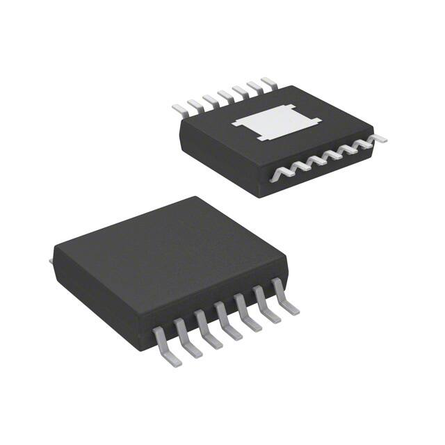
Device Information(1)
PART NUMBER
PACKAGE
BODY SIZE (NOM)
HTSSOP (14)
5.00 mm × 4.40 mm
2 Applications
LM5161
•
•
•
Industrial Programmable Logic Controller
IGBT Gate Drive Bias Supply
Telecom DC-DC Primary and Secondary Side
Bias
E-Meter Power Line Communication
Low-Power ( 72 V, an external VCC supply is commonly used to minimize the power
dissipation in the IC. In such applications at TJ >125°C, it is recommended to add a BST resistor (> 3Ω) in series
with the BST capacitor, in order to protect the internal VCC-BST diode during a full load transient operation. The
addition of the external resistor will reduce the fast (dv/dt) of the switch node that can impact the normal IC
operation.
If the FPWM pin is pulled high, the LM5161 will operate in CCM mode regardless of the load conditions. The
CCM operation reduces efficiency at light load but improves the output transient response to step load changes
and provides nearly constant switching frequency. Moreover, the Fly-Buck topology always requires the
continuous conduction mode during its operation.
The internal ripple injection circuit is disabled in the CCM mode. An external ripple injection circuit or an
additional ESR resistor in series with the output capacitor is required to generate the optimal ripple at the FB
node. Also, there is no need to add any BST resistor in series with the BST capacitor in either forced CCM Buck
or Fly-Buck application.
Table 1. FPWM Pin Mode Summary
FPWM PIN CONNECTION
LOGIC STAGE
DESCRIPTION
GND or Floating (High Z)
0
The FPWM pin is grounded or left floating. DCM enabled at light
loads. Internal Ripple circuit is enabled. No external ripple
circuit/ addition required.
VCC
1
The FPWM pin is connected to VCC. The LM5161 then operates
in CCM mode at light loads. Internal ripple injection disabled.
External ripple injection needed.
7.4.2 Undervoltage Detector
Table 2 summarizes the dual threshold levels of the under-voltage lockout (EN/UVLO) circuit explained in Enable
/ Undervoltage Lockout (EN/UVLO) .
Table 2. UVLO Pin Mode Summary
EN/UVLO PIN
VOLTAGE
VCC REGULATOR
MODE
< 0.35 V
Off
Shutdown
VCC regulator disabled. High and low side
FETs disabled.
0.35 V to 1.24 V
On
Standby
VCC regulator enabled. High and low side
FETs disabled.
VCC < VCC(UV)
Standby
VCC regulator enabled. High and low side
FETs disabled.
VCC > VCC(UV)
Operating
VCC regulator enabled. Switching enabled.
> 1.24 V
DESCRIPTION
If an EN/UVLO setpoint is not required, the EN/UVLO pin can be driven by a logic signal as an enable input or
connected directly to the VIN pin. If the EN/UVLO is directly connected to the VIN pin, the regulator will begin
switching when the VCC UVLO is satisfied.
Submit Documentation Feedback
Copyright © 2016–2017, Texas Instruments Incorporated
Product Folder Links: LM5161
15
�LM5161
SNVSAE3B – MARCH 2016 – REVISED NOVEMBER 2017
www.ti.com
8 Applications and Implementation
NOTE
Information in the following applications sections is not part of the TI component
specification, and TI does not warrant its accuracy or completeness. TI’s customers are
responsible for determining suitability of components for their purposes. Customers should
validate and test their design implementation to confirm system functionality.
8.1 Application Information
The LM5161 is a synchronous-buck regulator converter designed to operate over a wide input voltage and output
current range. Spreadsheet based Quick-Start Calculator tools, available on the www.ti.com product website, can
be used to design a single output synchronous buck converter or an isolated dual output Fly-Buck converter
using the LM5161. See application note Designing an Isolated Buck (Fly-Buck) Converter for a detailed design
guide for the Fly-Buck converter. Alternatively, the online WEBENCH® Tool can be used to create a complete
buck or Fly-Buck designs and generate the bill of materials, estimated efficiency, solution size, and cost of the
complete solution.Typical Applications describes a few application circuits using the LM5161 with detailed, stepby-step design procedures.
8.2 Typical Applications
8.2.1 LM5161 Synchronous Buck (15-V to 95-V Input, 12-V Output, 1-A Load)
A typical application example is a synchronous buck converter operating from a wide input voltage range of 15 V
to 95 V and providing a stable 12 V output voltage with maximum output current capability of 1 A. The complete
schematic for a typical buck application circuit with LM5161 in diode emulation is shown in Figure 25 . In the
application schematic below, the components are labeled by their respective component numbers instead of the
descriptive name used in the previous sections. For example, R1 represents RON and so on.
J4
1
2
D1
C1
U1
VIN 15 - 80VDC
SD103AWS-7-F
40V
0.01µF
2
1
3
R1
J1
C4
2.2µF
C6
2.2µF
C5
0.1µF
R3
75.0k
5
VIN
RON
402k
4
6
BST
SW
SW
EN/UVLO
FPWM
SS
VCC
13
12
L2
SW
1
2
15
GND
FB
AGND
PGND
PAD
NC
NC
R6
10
9
7
14
C7
1
2
R7
10.0k
1000pF
C10
0.1µF
J2
C11
10µF
C12
10µF
R8
2.00k
LM5161PWP
1
2
3
R9
6.81k
R4
0
C13
1µF
SW
GND
2
1
VOUT 12VDC
IOUT 1A
DR125-101-R
8
100k
C9
0.022uF
J3
R2
0
11
GND
GND
GND
JP1
GND
GND
Copyright © 2016, Texas Instruments Incorporated
Figure 25. Synchronous Buck Application Circuit with LM5161
16
Submit Documentation Feedback
Copyright © 2016–2017, Texas Instruments Incorporated
Product Folder Links: LM5161
�LM5161
www.ti.com
SNVSAE3B – MARCH 2016 – REVISED NOVEMBER 2017
Typical Applications (continued)
8.2.1.1 Design Requirements
A typical synchronous-buck application introduced in LM5161 Synchronous Buck (15-V to 95-V Input, 12-V
Output, 1-A Load) , Table 3 summarizes the operating parameters:
Table 3. Design Parameters
DESIGN PARAMETER
EXAMPLE VALUE
Input voltage range
15-V to 80-V
output
12-V
Full load current
1-A
Nominal switching frequency
300 kHz
Light load operating mode
CCM, FPWM=1
Jumper JP1
Pins 1-2 connected
8.2.1.2 Detailed Design Procedure
8.2.1.2.1 Custom Design With WEBENCH® Tools
Click here to create a custom design using the LM5161 device with the WEBENCH® Power Designer.
1. Start by entering the input voltage (VIN), output voltage (VOUT), and output current (IOUT) requirements.
2. Optimize the design for key parameters such as efficiency, footprint, and cost using the optimizer dial.
3. Compare the generated design with other possible solutions from Texas Instruments.
The WEBENCH Power Designer provides a customized schematic along with a list of materials with real-time
pricing and component availability.
In most cases, these actions are available:
• Run electrical simulations to see important waveforms and circuit performance
• Run thermal simulations to understand board thermal performance
• Export customized schematic and layout into popular CAD formats
• Print PDF reports for the design, and share the design with colleagues
Get more information about WEBENCH tools at www.ti.com/WEBENCH.
8.2.1.2.2 Output Resistor Divider Selection
With the required output voltage set point at 12 V and VFB = 2 V (typical), the ratio of R8 (RFB1) to R7 (RFB2) can
be calculated using Equation 6:
RFB2 VOUT
1
RFB1 VREF
(6)
The resistor ratio calculates to be 5:1. Standard values of R8 (RFB1) = 2 kΩ and R7 (RFB2 ) =10 kΩ are chosen.
Higher or lower resistor values could be used as long as the ratio of 5:1 is maintained.
8.2.1.2.3 Frequency Selection
The duty cycle required to maintain output regulation at the minimum input voltage restricts the maximum
switching frequency of LM5161. The maximum value of the minimum forced OFF-time TOFF,min (max), limits the
duty cycle and therefore the switching frequency. The maximum frequency that avoids output dropout at
minimum input voltage can be calculated from Equation 7.
VIN, min VOUT
FSW, max (@ VIN, min )
VIN, min u TOFF, min (ns)
(7)
For this design example, the maximum frequency based on the minimum OFF-time limitation for TOFF,min(typ) =
170 ns is calculated to be FSW,max(@VIN,min) = 1.2 MHz. This value is above 1 MHz, the maximum possible
operating frequency of the LM5161. Therefore, the minimum OFF-time parameter restricts the maximum
achievable switching frequency calculation in this application.
Submit Documentation Feedback
Copyright © 2016–2017, Texas Instruments Incorporated
Product Folder Links: LM5161
17
�LM5161
SNVSAE3B – MARCH 2016 – REVISED NOVEMBER 2017
www.ti.com
At the maximum input voltage, the maximum switching frequency of LM5161 is restricted by the minimum ONtime, TON,min which limits the minimum duty cycle of the converter. The maximum frequency at maximum input
voltage can be calculated using Equation 8.
VOUT
FSW, max (@ VIN, max )
VIN, max u TON, min (ns)
(8)
Using Equation 8 and TON,min (typ) = 150 ns, the maximum achievable switching frequency is FSW,max(@VIN,min)=
1000 kHz. Taking this value as the maximum possible operational switching frequency over the input voltage
range in this application, a nominal switching frequency of FSW = 300 kHz is chosen for this design.
The value of the resistor, RON sets the nominal switching frequency based on Equation 9.
VOUT
RON
:
1.008 x 10 10 x FSW
(9)
For this particular application with FSW = 300 kHz, RON calculates to be 396 kΩ . Selecting a standard value for
R1 (RON) = 402 kΩ (±1%) results in a nominal frequency of 296 kHz. The resistor value may need to adjusted
further in order to achieve the required switching frequency as the switching frequency in Constant ON-Time
converters varies slightly(±10%) with input voltage and/or output current. Operation at a lower nominal switching
frequency will result in higher efficiency but increase in the inductor and capacitor values leading to a larger total
solution size.
8.2.1.2.4 Inductor Selection
The inductor is selected to limit the inductor ripple current to a value between 20 and 40 percent of the maximum
load current. The minimum value of the inductor required in this application can be calculated from Equation 10:
VO u (VIN, max VO )
Lmin
VIN, max u FSW u IO, max u 0.4
(10)
Based on Equation 10 , the minimum value of the inductor is calculated to be 85 µH for VIN = 80-V (max) and
inductor current ripple will be 40 percent of the maximum load current. Allowing some margin for inductance
variation and inductor saturation, a higher standard value of L1 (L) = 100 µH is selected for this design.
The peak inductor current at maximum load must be smaller than the minimum current limit threshold of the high
side FET as given in Electrical Characteristics table. The inductor current ripple at any input voltage is given by:
VO u (VIN VO )
'IL
VIN u FSW u L
(11)
The peak-to-peak inductor current ripple is calculated to be 81 mA and 341 mA at the minimum and maximum
input voltages respectively. The maximum peak inductor current in the buck FET is given by Equation 12:
'IL, max
IL(peak) IO, max
(12)
2
In this design with maximum output current of 1-A, the maximum peak inductor current is calculated to be
approximately 1.17 A at VIN,max = 80 V, which is less than the minimum high-side FET current limit threshold.
The saturation current of the inductor must also be carefully considered. The peak value of the inductor current
will be bound by the high side FET current limit during overload or short circuit conditions. Based on the high
side FET current limit specification in the Electrical Characteristics, an inductor with saturation current rating
above 1.9 A (max) should be selected.
18
Submit Documentation Feedback
Copyright © 2016–2017, Texas Instruments Incorporated
Product Folder Links: LM5161
�LM5161
www.ti.com
SNVSAE3B – MARCH 2016 – REVISED NOVEMBER 2017
8.2.1.2.5 Output Capacitor Selection
The output capacitor is selected to limit the capacitive ripple at the output of the regulator. Maximum capacitive
ripple is observed at maximum input voltage. The output capacitance required for a ripple voltage ∆VO across the
capacitor is given by Equation 13.
'IL, max
COUT
8 u FSW u 'VO, ripple
(13)
Substituting ∆VO, ripple = 10 mV gives COUT = 15 μF. Two standard 10 μF ceramic capacitors in parallel (C11,
C12) are selected. An X7R type capacitor with a voltage rating 25 V or higher should be used for COUT (C11,
C12) to limit the reduction of capacitance due to dc bias voltage.
8.2.1.2.6 Series Ripple Resistor - RESR (FPWM = 1)
If the FPWM = 1, i.e. the FPWM pin is pulled high as when connected to VCC, a series resistor in series with the
output capacitor or the external ripple injection circuit must be selected such that sufficient ripple injection (>
25mV) is ensured at the feedback pin FB. The ripple produced by RESR is proportional to the inductor current
ripple, and therefore, RESR should be chosen for minimum inductor current ripple which occurs at minimum input
voltage. The RESR is calculated by Equation 14.
25 mV u VO
RESR t
VREF u 'IL, min
(14)
With VO = 12 V, VREF = 2 V and ΔIL, min = 81 mA (at VIN, min= 15 V) as calculated in Equation 11, Equation 14
requires an RESR greater than or equal to 1.87 Ω. Selecting R4 (RESR) = 2 Ω results in approximately 700 mV of
maximum output voltage ripple at VIN,max. However due to the internal DC Error correction loop, the load and line
regulation will be much improved, despite the addition of a large RESR in the circuit. For applications which
require even lower output voltage ripple, Type 2 or Type 3 ripple injection circuits must be used, as described in
Ripple Configuration. In this design example, with the FPWM =1 (i.e. the FPWM pin is pulled up to VCC) a 0 Ω
ESR resistor is selected and the external Type 3 ripple injection circuit is used.
8.2.1.2.7 VCC and Bootstrap Capacitor
The VCC capacitor charges the bootstrap capacitor during the OFF-time of the high-side switch and powers
internal logic circuits and the low side sync FET gate driver. The bootstrap capacitor biases the high-side gate
driver during the high-side FET ON-time. A good value for C13 (CVCC) is 1 µF. A good choice for C1 (CBST) is 10
nF. Both must be high quality X7R ceramic capacitors.
8.2.1.2.8 Input Capacitor Selection
The input capacitor must be large enough to limit the input voltage ripple to an acceptable level. Equation 15
provides the input capacitance CIN required for a worst case input ripple of ∆VIN, ripple.
IO, max u D u (1 D)
CIN
'VIN, ripple u FSW
(15)
CIN (C4, C6) supplies most of the switch current during the ON-time to limit the voltage ripple at the VIN pin. At
maximum load current, when the buck switch turns on, the current into the VIN pin quickly increases to the valley
current of the inductor ripple and then ramps up to the peak of the inductor ripple during the ON-time of the highside FET. The average current during the ON-time is the output load current. For a worst-case calculation, CIN
must supply this average load current during the maximum ON-time, without letting the voltage at VIN drop more
than the desired input ripple. For this design, the input voltage drop is limited to 0.5 V and the value of CIN is
calculated using Equation 15.
Based on Equation 15, the value of the input capacitor is calculated to be approximately 1.68 µF at D = 0.5.
Taking into account the decrease in capacitance over an applied voltage, two standard value ceramic capacitors
of 2.2 μF are selected for C4 and C6. The input capacitors should be rated for the maximum input voltage under
all operating and transient conditions. A 100-V, X7R dielectric was selected for this design.
A third input capacitor C5 is needed in this design as a bypass path for the high frequency component of the
input switching current. The value of C5 is 0.1 μF and this bypass capacitor must be placed directly across VIN
and PGND (pin 3 and 2) near the IC. The CIN values and location are critical to reducing switching noise and
transients.
Submit Documentation Feedback
Copyright © 2016–2017, Texas Instruments Incorporated
Product Folder Links: LM5161
19
�LM5161
SNVSAE3B – MARCH 2016 – REVISED NOVEMBER 2017
www.ti.com
8.2.1.2.9 Soft-Start Capacitor Selection
The capacitor at the SS pin determines the soft-start time, that is the time for the output voltage to reach its final
steady state value. The capacitor value is determined from Equation 16:
ISS u TStartup
CSS
VSS
(16)
With C9 (CSS) set at 22 nF and the Vss = 2 V, ISS = 10 µA, the TStartup should measure approximately 4 ms.
8.2.1.2.10 EN/UVLO Resistor Selection
The UVLO resistors R3 (RUV2) and R9 (RUV1) set the input undervoltage lockout threshold and hysteresis
according to Equation 17 and Equation 18:
VIN(HYS) IUVLO(HYS) u RUV2
(17)
and,
§ RUV2 ·
VUVLO(TH) ¨ 1
¸
RUV1 ¹
©
VIN, UVLO(rising)
(18)
From the Electrical Characteristics, IUVLO(HYS) = 20 μA (typical). To design for VIN rising threshold (VIN, UVLO(rising))
at 15 V and EN/UVLO hysteresis of 1.5 V, Equation 17 and Equation 18 yield RUV1 = 6.81 kΩ and RUV2 = 75 kΩ .
Selecting 1% standard value of R9 (RUV1) = 6.81 kΩ and R3 (RUV2) = 75 kΩ results in UVLO threshold (rising)
and hysteresis of 14.9 V and 1.5 V respectively.
8.2.1.3 Application Curves
12.12
100
12.1
Ext-VCC
12.08
95
12.04
Efficiency (%)
Output Voltage (V)
12.06
12.02
12
11.98
11.96
90
85
Int-VCC
Ext-VCC
FPWM = 1
11.94
VIN = 24 V
VIN = 48 V
VIN = 60 V
11.92
11.9
80
FPWM = 1
11.88
0
0.1
0.2
0.3
0.4 0.5 0.6
Load Current (A)
0.7
0.8
0.9
1
75
0
0.1
Figure 26. Load Regulation
20
VIN = 24 V
VIN = 48 V
VIN = 60 V
Submit Documentation Feedback
0.2
0.3
0.4 0.5 0.6 0.7 0.8
Load Current (A)
Figure 27. Efficiency vs IOUT (FPWM = 1)
0.9
1
Copyright © 2016–2017, Texas Instruments Incorporated
Product Folder Links: LM5161
�LM5161
www.ti.com
SNVSAE3B – MARCH 2016 – REVISED NOVEMBER 2017
Figure 28. EN/UVLO Start-up at VIN= 48 V and IOUT = 1 A
Figure 29. Pre-Bias (11.5 V) Start-up at VIN= 48 V at No
Load & FPWM = 1
Figure 30. EN/UVLO Start-up at VIN= 48 V and RLOAD = 12 Ω
at FPWM = 1
Figure 31. Load Transient (0 A - 1 A) at VIN = 48 V
at FPWM = 0
Figure 32. Load Transient (0 A - 1 A) at VIN = 48 V
at FPWM = 1
Figure 33. Output Short-Circuit at VIN = 48 V
(Full Load to Short)
Submit Documentation Feedback
Copyright © 2016–2017, Texas Instruments Incorporated
Product Folder Links: LM5161
21
�LM5161
SNVSAE3B – MARCH 2016 – REVISED NOVEMBER 2017
www.ti.com
8.2.2 LM5161 Isolated Fly-Buck (36-V to 72-V Input, 12-V, 12-W Isolated Output)
A typical application example for an isolated Fly-Buck converter operates over an input voltage range of 36 V to
72 V. It provides a stable 12 V isolated output voltage with output power capability of 10 W. The complete
schematic of the Fly-Buck application circuit is shown in Figure 34.
C1
2200pF
GND
ISOGND
R1
0
C2
10µF
C3
10µF
1
2
R2
2.00k
J1
D1
MBR1H100SFT3G
6
7
5
NC
NC
8
VOUTISO
C17
2200pF
T1
60µH
GND
1
2
C4
3
R4
R5
100k
36-72VIN
C8
2.2µF
J2
C9
2.2µF
5
VIN
RON
402k
C10
0.1µF
4
2
1
6
BST
SW
SW
EN/UVLO
FPWM
SS
VCC
4
3
TP1
U1
VIN
R3
11
13
12
0
0.01µF
SW
R6
100k
VOUT
C5
1000pF
J3
VOUT
8
D2
C11
0.1µF
10
1
2
R7
10.7k
C12
10µF
C13
10µF
VPRI
SD103AWS-7-F
R9
3.57k
1
2
15
C14
0.022µF
J4
1
FB
AGND
PGND
PAD
NC
NC
12VSEC
9
7
14
C15
1µF
R10
2.00k
GND
LM5161PWPR
1040
GND
GND
GND
GND
GND
SW
GND
GND
Copyright © 2016, Texas Instruments Incorporated
Figure 34. 12-V, 10-W Fly-Buck Schematic
8.2.2.1 LM5161 Fly-Buck Design Requirements
The LM5161 Fly-Buck application example is designed to operate from a nominal 48-V DC supply with line
variations from 36-V to 72-V. This example provides a space-optimized and efficient 12-V isolated output solution
with secondary load current capability from 0-A to 800 mA. The primary side remains unloaded in this
application. The switching frequency is set at 300 kHz (nominal). This design achieves greater than 88% peak
efficiency.
Table 4. Design Parameters
DESIGN PARAMETER
EXAMPLE VALUE
Input voltage range
36 V - 72 V
Isolated output
12 V (+/- 10%)
Isolated load current range (IISO)
0-A to 0.8-A
Nominal switching frequency
300 KHz
Peak efficiency
~87%
Operation mode
FPWM = 1
8.2.2.2 Detailed Design Procedure
The Fly-Buck converter design procedure closely follows the buck converter design outlined in LM5161
Synchronous Buck (15-V to 95-V Input, 12-V Output, 1-A Load) . The selection of primary output voltage,
transformer turns ratio, rectifier diode, and output capacitors are covered here.
8.2.2.2.1 Selection of VOUT and Turns Ratio
The primary output voltage in a Fly-Buck converter should be no more than one half of the minimum input
voltage. Therefore, at the minimum VIN of 36 V, the primary output voltage ( VOUT ) should be no higher than 18
V. The isolated output voltage of VOUTISO in Figure 34 is set at 12 V by selecting a transformer with a turns ratio
(N1:N2 :: NPRI:NSEC) of 1:1. Using this turns ratio, the required primary output voltage VOUT is calculated in
Equation 19:
22
Submit Documentation Feedback
Copyright © 2016–2017, Texas Instruments Incorporated
Product Folder Links: LM5161
�LM5161
www.ti.com
VOUT
SNVSAE3B – MARCH 2016 – REVISED NOVEMBER 2017
VOUTISO VFD1
N2
N1
VOUTISO 0.7V
1
12.7 V
(19)
The 0.7 V (VFD1) added to VOUTISO in Equation 19 represents the forward voltage drop of the secondary rectifier
diode. By setting the primary output voltage VOUT to 12.7-V by selecting the correct feedback resistors, the
secondary voltage is regulated at 12-V nominally. Adjustment of the primary side VOUT may be required to
compensate for voltage errors due to the leakage inductance of the transformer, the resistance of the transformer
windings, the diode drop in the power path on the secondary side and the low-side FET of the LM5161.
8.2.2.2.2 Secondary Rectifier Diode
The secondary side rectifier diode must block the maximum input voltage reflected at secondary side switch
node. The minimum diode reverse voltage V(RD1) rating is given in Equation 20:
N
VRD1 VIN(max) x 2 VOUTISO 72V x 1 12V 84V
N1
(20)
A diode of 100-V or higher reverse voltage rating must be selected in this application. If the input voltage (VIN)
has transients above the normal operating maximum input voltage of 72 V, then the worst-case transient input
voltage must be used in the Equation 20 while selecting the secondary side rectifier diode.
8.2.2.2.3 External Ripple Circuit
The FPWM pin in the LM5161 should never be grounded or left open when used in a Fly-Buck application. Type
3 ripple circuit is required for Fly-Buck applications. Follow the design procedure used in the buck converter for
selecting the Type 3 ripple injection components. See Ripple Configuration for ripple design information.
8.2.2.2.4 Output Capacitor (CVISO)
The Fly-Buck output capacitor conducts higher ripple current than a buck converter output capacitor. The ripple
voltage across the isolated output capacitor is calculated based on the time the rectifier diode is off. During this
time the entire output current is supplied by the output capacitor. The required capacitance for the worst-case
ripple voltage can be calculated using Equation 21 where, ΔVISO is the expected ripple voltage at the secondary
output.
IISO § VPRI · 1
CVISO
¨
¸u
'VISO ¨© VIN(MIN) ¸¹ fsw
(21)
Equation 21 is an approximation and ignores the ripple components associated with ESR and ESL of the output
capacitor. For a ΔVISO = 100 mV, Equation 21 requires CVISO = 11.12 µF. When selecting the CVISO output
capacitors (C2 and C3 in the Figure 34), the DC bias must be considered in order to ensure sufficient
capacitance over the output voltage.
Submit Documentation Feedback
Copyright © 2016–2017, Texas Instruments Incorporated
Product Folder Links: LM5161
23
�LM5161
SNVSAE3B – MARCH 2016 – REVISED NOVEMBER 2017
www.ti.com
8.2.2.3 Application Curves
100
VIN= 36 V
VIN= 48 V
VIN= 72 V
12.8
12.4
12
11.6
80
70
60
11.2
10.8
VIN= 36 V
VIN= 48 V
VIN= 72 V
50
0
24
90
Efficiency (%)
Isolated Secondary Output Voltage (V)
13.2
0.1
0.2
0.3
0.4
0.5
0.6
Isolated Secondary Load Current (A)
0.7
0.8
0
0.1
0.2
0.3
0.4
0.5
0.6
Isolated Secondary Load Current (A)
0.7
Figure 35. Load Regulation
Figure 36. Efficiency vs IISO
Figure 37. Steady State at VIN = 48 V
and IOUT2 = 500 mA
Figure 38. Secondary Load Transient
at IISO = 250 mA - 750 mA
Figure 39. VIN Start-up at IISO = 500 mA
Figure 40. Secondary-Side Short at IOUT2 = 0 A
and IPRI = 0 A
Submit Documentation Feedback
0.8
Copyright © 2016–2017, Texas Instruments Incorporated
Product Folder Links: LM5161
�LM5161
www.ti.com
SNVSAE3B – MARCH 2016 – REVISED NOVEMBER 2017
8.2.3 Ripple Configuration
LM5161 uses a Constant-On-Time (COT) control scheme, in which the ON-time is terminated by a one-shot, and
the OFF-time is terminated by the feedback voltage (VFB) falling below the reference voltage. Therefore, for
stable operation, the feedback voltage must decrease monotonically and in phase with the inductor current
during the OFF-time. Furthermore, this change in feedback voltage (VFB) during OFF-time must be large enough
to dominate any noise present at the feedback node.
Table 5 presents three different methods for generating appropriate voltage ripple at the feedback node. Type 1
and Type 2 ripple circuits couple the ripple from the output of the converter to the feedback node (FB). The
output voltage ripple has two components:
1. Capacitive ripple caused by the inductor current ripple charging or discharging the output capacitor.
2. Resistive ripple caused by the inductor current ripple flowing through the ESR of the output capacitor and
R3.
The capacitive ripple is out-of-phase with the inductor current. As a result, the capacitive ripple does not
decrease monotonically during the OFF-time. The resistive ripple is in phase with the inductor current and
decreases monotonically during the OFF-time. The resistive ripple must exceed the capacitive ripple at output
(VOUT) for stable operation. If this condition is not satisfied unstable switching behavior is observed in COT
converters, with multiple ON-time bursts in close succession followed by a long OFF-time.
Type 3 ripple method uses a ripple injection circuit with RA, CA and the switch node (SW) voltage to generate a
triangular ramp. This triangular ramp is then AC-coupled into the feedback node (FB) using the capacitor CB.
Because this circuit does not use the output voltage ripple, it is suited for applications where low output voltage
ripple is imperative. See application note Controlling Output Ripple and Achieving ESR Independence in
Constant On-Time (COT) Regulator Designs for more details for each ripple generation method.
Table 5. Ripple Configuration
TYPE 1
TYPE 2
TYPE 3
Lowest Cost
Reduced Ripple
Minimum Ripple
VOUT
VOUT
L1
R FB2
R3
Cff
To FB
R FB2
RA
R3
R FB1
C OUT
To FB
R FB1
GND
GND
Copyright © 2016, Texas Instruments Incorporated
Copyright © 2016, Texas Instruments Incorporated
25 mV u VO
VREF u 'IL1, min
COUT
R FB2
GND
C OUT
Cff t
CA
CB
To FB
R FB1
R3 t
VOUT
L1
L1
Copyright © 2016, Texas Instruments Incorporated
5
FSW u (RFB2 IIRFB1 )
R A CA d
(22) R t 25 mV
3
'IL1, min
(VIN, min
VO ) u TON(@ VIN, min )
25mV
(24)
(23)
8.3 Do's and Don'ts
As mentioned earlier in Soft-Start , the SS capacitor CSS, must be more than 1 nF in both Buck and Fly-Buck
applications. Apart from determining the start-up time, this capacitor serves for the external compensation of the
internal GM error amplifier. A minimum value of 1 nF is necessary to maintain stability. The SS pin must not be
left floating.
When the FPWM pin is shorted to ground or left unconnected, no external ripple injection is necessary in a Buck
application. Should an external feedback ripple circuit be configured when FPWM = 0, it will produce higher
ripple at the output.
Submit Documentation Feedback
Copyright © 2016–2017, Texas Instruments Incorporated
Product Folder Links: LM5161
25
�LM5161
SNVSAE3B – MARCH 2016 – REVISED NOVEMBER 2017
www.ti.com
Do's and Don'ts (continued)
Add a resistor (>3Ω) in series with the BST capacitor when using the part in FPWM = 0, as described in detail in
Forced Pulse Width Modulation (FPWM) Mode.
When configured as a Fly-Buck, the FPWM pin must always be connected to VCC. A Fly-Buck application must
operate in the continuous conduction mode all the time in order to maintain adequate voltage regulation on the
secondary side. FPWM = 0 is not a valid mode in the Fly-Buck application.
9 Power Supply Recommendations
The LM5161 is designed to operate with an input power supply capable of supplying a voltage range between
4.5 V and 100 V. The power supply should be well regulated and capable of supplying sufficient current to the
regulator during the sync buck mode or the isolated Fly-Buck mode of operation. As in all DC/DC applications,
the power supply source impedance must be small compared to the converter input impedance in order to
maintain the stability of the converter.
If the LM5161 is used in a buck topology with low input supply voltage (4.5 V) and large load current (1 A), it is
prudent to add a large electrolytic capacitor, in parallel the CIN capacitors. The electrolytic capacitor stabilizes the
input voltage to the IC and prevent droop or oscillation, over the entire load range. Also, it is necessary to add
the electrolytic capacitor or a ceramic capacitor in series with appropriate ESR, parallel to the input capacitors
CIN, in order to dampen the input voltage spikes, as detected by the LM5161 when connected to a power supply
with long power leads. These input voltage spikes can easily be twice the input voltage step amplitude and a
damping capacitor is necessary to contain the input voltage to less than 100V in order to protect the LM5161.
10 Layout
10.1 Layout Guidelines
A proper layout is essential for optimum performance of the circuit. In particular, observe the following layout
guidelines:
• CIN: The loop consisting of input capacitor (CIN), VIN pin, and PGND pin carries the switching current.
Therefore, in the LM5161, the input capacitor must be placed close to the IC, directly across VIN and PGND
pins, and the connections to these two pins should be direct to minimize the loop area. In general it is not
possible to place all of input capacitances near the IC. However, a good layout practice includes placing the
bulk capacitor as close as possible to the VIN pin (see Figure 41). When using the LM5161 HTSSOP-14
package, a bypass capacitor (Cbyp) measuring ~0.1 μF must be placed directly across VIN and PGND (pin 3
and 2), as close as possible to the IC while complying with all layout design rules.
• The RON resistor between the VIN and the RON pin and the SS capacitor should be placed as close as
possible to their respective pins.
• CVCC and CBST: The VCC and bootstrap (BST) bypass capacitors supply switching currents to the high-side
and low-side gate drivers. These two capacitors should also be placed as close to the IC as possible, and the
connecting trace lengths and the loop area must be kept at minimum (see Figure 41).
• The feedback trace carries the output voltage information and a small ripple component that is necessary for
proper operation of the LM5161. Therefore, care must be taken while routing the feedback trace to avoid
coupling any noise into this pin. In particular, the feedback trace must be short and not run close to magnetic
components, or parallel to any other switching trace.
• In FPWM=1 mode, if a ripple injection circuit is being used for ripple generation at the FB pin, it is considered
a good layout practice to lay out the feedback ripple injection DC trace and the VOUT trace differentially. This
scheme helps in reducing the scope for any noise injection at the FB pin.
• SW trace: The SW node switches rapidly between VIN and GND every cycle and is therefore a source of
noise. The SW node area must be kept at minimum. In particular, the SW node should not be inadvertently
connected to a copper plane or pour.
26
Submit Documentation Feedback
Copyright © 2016–2017, Texas Instruments Incorporated
Product Folder Links: LM5161
�LM5161
www.ti.com
SNVSAE3B – MARCH 2016 – REVISED NOVEMBER 2017
10.2 Layout Example
VOUT
CA
COUT
LIND
GND
Cbyp
AGND
NC
PGND
SW
SW
VIN
SW
SW
RA
CIN
VLINE
EN/
UVLO
RUV
RON
SW
CBST
LM5161
BST
CVCC
EXP PAD
RON
VCC
CB
SS
FB
NC
FPWM
FPWM
CSS
RFB2
RFB1
Via to Ground Plane
Copyright © 2016, Texas Instruments Incorporated
Figure 41. Typical Buck Layout Example with the LM5161
Submit Documentation Feedback
Copyright © 2016–2017, Texas Instruments Incorporated
Product Folder Links: LM5161
27
�LM5161
SNVSAE3B – MARCH 2016 – REVISED NOVEMBER 2017
www.ti.com
11 Device and Documentation Support
11.1 Custom Design With WEBENCH® Tools
Click here to create a custom design using the LM5161 device with the WEBENCH® Power Designer.
1. Start by entering the input voltage (VIN), output voltage (VOUT), and output current (IOUT) requirements.
2. Optimize the design for key parameters such as efficiency, footprint, and cost using the optimizer dial.
3. Compare the generated design with other possible solutions from Texas Instruments.
The WEBENCH Power Designer provides a customized schematic along with a list of materials with real-time
pricing and component availability.
In most cases, these actions are available:
• Run electrical simulations to see important waveforms and circuit performance
• Run thermal simulations to understand board thermal performance
• Export customized schematic and layout into popular CAD formats
• Print PDF reports for the design, and share the design with colleagues
Get more information about WEBENCH tools at www.ti.com/WEBENCH.
11.2 Related Documentation
•
•
•
AN-2292 Designing an Isolated Buck (Fly-Buck) Converter
AN-1481 Controlling Output Ripple & Achieving ESR Independence in Constant On-Time Regulator Designs
AN-1481 Controlling Output Ripple & Achieving ESR Independence in Constant On-Time Regulator Designs
AN-1481 Controlling Output Ripple & Achieving ESR Independence in Constant On-Time Regulator Designs
application report,
11.3 Receiving Notification of Documentation Updates
To receive notification of documentation updates, navigate to the device product folder on ti.com. In the upper
right corner, click on Alert me to register and receive a weekly digest of any product information that has
changed. For change details, review the revision history included in any revised document.
11.4 Community Resources
The following links connect to TI community resources. Linked contents are provided "AS IS" by the respective
contributors. They do not constitute TI specifications and do not necessarily reflect TI's views; see TI's Terms of
Use.
TI E2E™ Online Community TI's Engineer-to-Engineer (E2E) Community. Created to foster collaboration
among engineers. At e2e.ti.com, you can ask questions, share knowledge, explore ideas and help
solve problems with fellow engineers.
Design Support TI's Design Support Quickly find helpful E2E forums along with design support tools and
contact information for technical support.
11.5 Trademarks
E2E is a trademark of Texas Instruments.
WEBENCH is a registered trademark of Texas Instruments.
11.6 Electrostatic Discharge Caution
These devices have limited built-in ESD protection. The leads should be shorted together or the device placed in conductive foam
during storage or handling to prevent electrostatic damage to the MOS gates.
11.7 Glossary
SLYZ022 — TI Glossary.
This glossary lists and explains terms, acronyms, and definitions.
28
Submit Documentation Feedback
Copyright © 2016–2017, Texas Instruments Incorporated
Product Folder Links: LM5161
�LM5161
www.ti.com
SNVSAE3B – MARCH 2016 – REVISED NOVEMBER 2017
12 Mechanical, Packaging, and Orderable Information
The following pages include mechanical packaging and orderable information. This information is the most
current data available for the designated devices. This data is subject to change without notice and revision of
this document. For browser-based versions of this data sheet, refer to the left-hand navigation.
Submit Documentation Feedback
Copyright © 2016–2017, Texas Instruments Incorporated
Product Folder Links: LM5161
29
�PACKAGE OPTION ADDENDUM
www.ti.com
10-Dec-2020
PACKAGING INFORMATION
Orderable Device
Status
(1)
Package Type Package Pins Package
Drawing
Qty
Eco Plan
(2)
Lead finish/
Ball material
MSL Peak Temp
Op Temp (°C)
Device Marking
(3)
(4/5)
(6)
LM5161PWPR
ACTIVE
HTSSOP
PWP
14
2500
RoHS & Green
SN
Level-3-260C-168 HR
-40 to 125
LM5161
PWP
LM5161PWPT
ACTIVE
HTSSOP
PWP
14
250
RoHS & Green
SN
Level-3-260C-168 HR
-40 to 125
LM5161
PWP
(1)
The marketing status values are defined as follows:
ACTIVE: Product device recommended for new designs.
LIFEBUY: TI has announced that the device will be discontinued, and a lifetime-buy period is in effect.
NRND: Not recommended for new designs. Device is in production to support existing customers, but TI does not recommend using this part in a new design.
PREVIEW: Device has been announced but is not in production. Samples may or may not be available.
OBSOLETE: TI has discontinued the production of the device.
(2)
RoHS: TI defines "RoHS" to mean semiconductor products that are compliant with the current EU RoHS requirements for all 10 RoHS substances, including the requirement that RoHS substance
do not exceed 0.1% by weight in homogeneous materials. Where designed to be soldered at high temperatures, "RoHS" products are suitable for use in specified lead-free processes. TI may
reference these types of products as "Pb-Free".
RoHS Exempt: TI defines "RoHS Exempt" to mean products that contain lead but are compliant with EU RoHS pursuant to a specific EU RoHS exemption.
Green: TI defines "Green" to mean the content of Chlorine (Cl) and Bromine (Br) based flame retardants meet JS709B low halogen requirements of