LM5170
SNVSBJ0B – DECEMBER 2019 – REVISED AUGUST 2021
LM5170 Multiphase Bidirectional Current Controller
1 Features
2 Applications
•
•
•
•
•
•
•
•
•
Functional Safety-Capable
– Documentation available to aid functional safety
system design
Suited for high power industrial dual battery
system
– 100-V HV-port and 65-V LV-port max ratings
– 1% Accurate bidirectional current regulation
– 1% Accurate channel current monitoring
– 5-A Peak half-bridge gate drivers
– Support multi-phase operation with stackability
– Diode emulation prevents negative current
Programmability and flexibility
– Programmable or adaptive dead-time control
– Programmable oscillator frequency with
optional synchronization to external clock
– Dual channel enable control inputs
– Analog and PWM current controls
– Programmable peak current limit
– Programmable soft-start timer
– Phase adding or dropping using EN2
Integrated protection features
– HV and LV port over-voltage protection
– MOSFET failure detect at start-up and circuit
breaker control
– Thermal shutdown
Battery tester
Bi-directional battery management system
Backup battery powered converters
Stackable buck or boost converters
Negative to positive voltage converter
3 Description
The LM5170 controller provides the essential high
voltage and precision elements of a dual-channel
bidirectional converter. It regulates the average
current flowing between the high voltage and low
voltage ports in the direction designated by the
DIR input signal. The current regulation level is
programmed through analog or digital PWM inputs.
Dual-channel differential current sense amplifiers and
dedicated channel current monitors achieve typical
current accuracy of 1%. Robust 5-A half-bridge
gate drivers are capable of driving parallel MOSFET
switches delivering 500 W or more per channel.
The diode emulation mode of the synchronous
rectifiers prevents negative currents but also enables
discontinuous mode operation for improved efficiency
with light loads. Versatile protection features include
cycle-by-cycle current limiting, overvoltage protection
at both HV and LV ports, MOSFET failure detection,
and overtemperature protection.
Device Information(1)
(1)
PART NUMBER
PACKAGE
BODY SIZE (NOM)
LM5170
TQFP (48)
7.00 mm × 7.00 mm
For all available packages, see the orderable addendum at
the end of the data sheet.
LV-Port
(12 V)
HV-Port
(48 V)
+10 V Bias
HO1 SW1 LO1
PGND
VCC
CSA1
VIN
CSB1
VINX
IOUT1
RAMP1
OVPA
IOUT2
IPK
OSC
RAMP2
SYNCOUT
AGND
ISETD
OVPB
SYNCIN
ISETA
DIR
EN1
CSB2
EN2
CSA2
HO2
SW2 LO2
GND
Simplified Application Circuit
Channel Current Tracking ISETA Command
An IMPORTANT NOTICE at the end of this data sheet addresses availability, warranty, changes, use in safety-critical applications,
intellectual property matters and other important disclaimers. PRODUCTION DATA.
�LM5170
www.ti.com
SNVSBJ0B – DECEMBER 2019 – REVISED AUGUST 2021
Table of Contents
1 Features............................................................................1
2 Applications..................................................................... 1
3 Description.......................................................................1
4 Revision History.............................................................. 2
5 Description (continued).................................................. 2
6 Pin Configuration and Functions...................................3
7 Specifications.................................................................. 6
7.1 Absolute Maximum Ratings........................................ 6
7.2 ESD Ratings............................................................... 6
7.3 Recommended Operating Conditions.........................6
7.4 Thermal Information....................................................7
7.5 Electrical Characteristics.............................................7
7.6 Typical Characteristics.............................................. 11
8 Detailed Description......................................................14
8.1 Overview................................................................... 14
8.2 Functional Block Diagram......................................... 15
8.3 Feature Description...................................................16
8.4 Device Functional Modes..........................................32
8.5 Programming............................................................ 36
9 Application and Implementation.................................. 39
9.1 Application Information............................................. 39
9.2 Typical Application.................................................... 47
10 Power Supply Recommendations..............................59
11 Layout........................................................................... 60
11.1 Layout Guidelines................................................... 60
11.2 Layout Examples.....................................................61
12 Device and Documentation Support..........................64
12.1 Device Support....................................................... 64
12.2 Receiving Notification of Documentation Updates..64
12.3 Support Resources................................................. 64
12.4 Trademarks............................................................. 64
12.5 Electrostatic Discharge Caution..............................64
12.6 Glossary..................................................................64
13 Mechanical, Packaging, and Orderable
Information.................................................................... 64
4 Revision History
Changes from Revision A (June 2020) to Revision B (August 2021)
Page
• Updated the numbering format for tables, figures and cross-references throughout the document ..................1
Changes from Revision * (November 2019) to Revision A (June 2020)
Page
• Added functional safety bullet to the Section 1 ..................................................................................................1
5 Description (continued)
An innovative average current mode control scheme maintains constant loop gain, allowing a single R-C network
to compensate both buck and boost conversion. The oscillator is adjustable up to 500 kHz and can synchronize
to an external clock. Multiphase parallel operation is achieved by connecting two LM5170 controllers for 3or 4-phase operation, or by synchronizing multiple controllers to phase-shifted clocks for a higher number of
phases. A low state on the UVLO pin disables the LM5170 in a low current shutdown mode.
2
Submit Document Feedback
Copyright © 2021 Texas Instruments Incorporated
Product Folder Links: LM5170
�LM5170
www.ti.com
SNVSBJ0B – DECEMBER 2019 – REVISED AUGUST 2021
DT
OSC
AGND
ISETA
DIR
EN2
ISETD
SYNCOUT
SYNCIN
EN1
IOUT2
IOUT1
48
47
46
45
44
43
42
41
40
39
38
37
6 Pin Configuration and Functions
NC
7
30
IPK
RAMP2
8
29
OPT
OVPA
9
28
RAMP1
UVLO
10
27
nFAULT
COMP2
11
26
COMP1
SS
12
25
OVPB
24
VCCA
SW1
31
23
6
HB1
VIN
22
NC
HO1
32
21
5
NC
NC
20
BRKS
LO1
33
19
4
VCC
VINX
18
BRKG
PGND
34
17
3
LO2
NC
16
CSB1
NC
35
15
2
HO2
CSB2
14
CSA1
HB2
36
13
1
SW2
CSA2
Figure 6-1. 48-Pin TQFP, PHP Package (Top View)
Table 6-1. Pin Functions
PIN
I/O(1)
DESCRIPTION
CSA2
I
2
CSB2
I
CH-2 differential current sense inputs. The CSA2 pin connects to the CH-2 power inductor. The CSB2 pin
connects to the circuit breaker or directly to the LV-Port if the circuit breaker is not used. The CH-2 current sense
resistor is placed between these two pins.
3
NC
—
No connect
NO.
NAME
1
4
VINX
O
Internally connected to VIN the pin through a cutoff switch. When the controller is shut down, VINX is
disconnected from VIN, opening the current leakage path. When the controller is enabled, VINX is connected
to VIN and serves as the pullup supply for the RC ramp generators at the RAMP1 and RAMP2 pins. VINX also
pulls up the OVPA pin through an internal 3-MΩ resistor.
5
NC
—
No connect
6
VIN
I
7
NC
—
The input pin connecting to the HV-Port line voltage. It supplies the BRKG pin through an internal 330-µA
current source.
No connect
Submit Document Feedback
Copyright © 2021 Texas Instruments Incorporated
Product Folder Links: LM5170
3
�LM5170
www.ti.com
SNVSBJ0B – DECEMBER 2019 – REVISED AUGUST 2021
Table 6-1. Pin Functions (continued)
PIN
DESCRIPTION
NAME
8
RAMP2
I
The inverting input of the CH-2 PWM comparator. An external RC circuit tied between VINX, RAMP2, and
AGND forms the ramp generator, producing a ramp signal proportional to the HV-Port voltage, thus achieving
a voltage feedforward function. The RAMP2 capacitor voltage is reset to AGND at the end of every switching
cycle.
9
OVPA
I
Connected to the non-inverting input of the HV-Port overvoltage comparator. An internal 3-MΩ pullup resistor
and an external resistor across the OVPA and AGND pins form a divider that senses the HV-Port voltage. When
the OVPA pin voltage is above the 1.185-V threshold, the SS capacitor is discharged and held low until the
overvoltage condition is removed.
10
ULVO
I
The UVLO pin serves as the master enable pin. When UVLO is pulled below 1.25 V, the entire LM5170 is in a
low quiescent current shutdown mode. When UVLO is pulled above 1.25 V but below 2.5 V, the LM5170 enters
the initialization stage where the nFAULT pin is first pulled up to 5 V, while the rest of the LM5170 is kept in
the OFF state. When UVLO is pulled above the 2.5 V, the LM5170 enters a MOSFET failure detection stage. If
no failure is detected, the circuit breaker gate driver (BRKS and BRKG) turns on, and the LM5170 enables the
oscillator and RAMP generator, and stands by until the EN1 and EN2 commands enable the channel.
11
COMP2
O
The output of the CH-2 transconductance (gm) error amplifier and the non-inverting input of the CH-2 PWM
comparator. A loop compensation network must be connected to this pin.
12
SS
I
The soft-start programming pin. An external capacitor and an internal 25-μA current source set the ramp rate of
the COMP pins voltage during soft start. If CH-2 is enabled after CH-1 completes soft start, the CH-2 turnon is
not controlled by the SS pin.
13
SW2
I
CH-2 switch node. Connect to the CH-2 high-side MOSFET source, the low-side MOSFET drain, and the
bootstrap capacitor return terminal.
CH-2 high-side gate driver bootstrap supply input
14
HB2
P
15
HO2
I/O
CH-2 high-side gate driver output
16
NC
—
No connect
17
LO2
I/O
CH-2 low-side gate driver output
18
PGND
G
Power ground connection pin for the low-side gate drivers and external VCC bias supply
19
VCC
I/P
VCC bias supply pin, powering the drivers. An external bias supply between 9 V to 12 V must be applied across
the VCC and PGND pins.
20
LO1
I/O
CH-1 low-side gate driver output
21
NC
—
No connect
22
HO1
I/O
CH-1 high-side gate driver output
23
HB1
P
CH-1 high-side gate driver bootstrap supply input
24
SW1
I
CH-1 switch node. Connect to the CH-1 high-side MOSFET source, the low-side MOSFET drain, and the
bootstrap capacitor return terminal.
25
OVPB
I
Connected to the non-inverting input of the LV-Port overvoltage comparator. An internal 1-MΩ pullup resistor
and an external resistor across the OVPB and AGND pins form the divider that senses the LV-Port voltage.
When the converter operates in boost mode, the OVPB pin status is ignored. In buck mode, when the OVPB
pin voltage is above the 1.185-V threshold, the SS capacitor is discharged and held low until the overvoltage
condition is removed.
26
COMP1
O
Output of the CH-1 transconductance (gm) error amplifier and the non-inverting input of the CH-1 PWM
comparator. A loop compensation network must be connected to this pin.
I/O
Fault flag pin or external shutdown pin. When a MOSFET drain-to-source short circuit failure is detected before
start-up, the nFAULT pin is internally pulled low to report the short-circuit failure. The LM5170 remains in a
disabled state. The nFAULT pin can also be externally pulled low to shut down the LM5170, serving as a forced
shutdown pin. In forced shutdown, all gate drivers turn off and nFAULT is latched low until the UVLO pin is
pulled below 1.25 V to release the latch and initiate a new start-up.
27
4
I/O(1)
NO.
nFAULT
28
RAMP1
I
The inverting input of the CH-1 PWM comparator. An external RC circuit tied between VINX, RAMP1, and
AGND forms the ramp generator, producing a ramp signal proportional to the HV-Port voltage. This achieves
a voltage feedforward function. The RAMP1 capacitor voltage is reset to AGND at the end of every switching
cycle.
29
OPT
I
Multiphase configuration pin. Tied to either VCCA or AGND, the OPT pin sets the phase lag of the SYNCOUT
signal corresponding to 4-phase or 3-phase operation, respectively.
30
IPK
I
A resistor connected between IPK and AGND sets the threshold for the cycle-by-cycle current limit comparator.
Submit Document Feedback
Copyright © 2021 Texas Instruments Incorporated
Product Folder Links: LM5170
�LM5170
www.ti.com
SNVSBJ0B – DECEMBER 2019 – REVISED AUGUST 2021
Table 6-1. Pin Functions (continued)
PIN
I/O(1)
DESCRIPTION
NO.
NAME
31
VCCA
I/P
Analog bias supply pin. Connect VCCA to VCC through an external 25-Ω resistor. A low-pass filter capacitor is
required from the VCCA pin to AGND.
32
NC
—
No connect
33
BRKS
O
Connect to the common source of the circuit breaker MOSFET pair. When the circuit breaker function is
disabled, simply connect to AGND through a 20-kΩ resistor.
34
BRKG
O
Connect to the gate pins of the circuit breaker MOSFET pair. Once the LM5170 is enabled, an internal 330-µA
current source starts to charge the circuit breaker MOSFET gates. The BRKG to BRKS voltage is internally
clamped at 12 V.
35
CSB1
I
36
CSA1
I
37
IOUT1
O
CH-1 inductor current monitor pin. A current source proportional to the CH-1 inductor current flows out of this
pin. Placing a terminating resistor and filter capacitor from IOUT1 to AGND produces a DC voltage representing
the CH-1 DC current level. An internal 25-µA offset DC current source at the IOUT1 pin raises the active signal
to be above the ground noise, thus improving the monitor noise immunity.
38
IOUT2
O
CH-2 inductor current monitor pin. A current proportional to the CH-2 inductor current flows out of this pin.
Placing a terminating resistor and filter capacitor from IOUT2 to AGND produces a DC voltage representing the
CH-2 DC current level. An internal 25-µA offset DC current source at the IOUT2 pin raises the active signal
above the ground noise, thus improving the monitor noise immunity.
39
EN1
I
CH-1 enable pin. Pulling EN1 above 2.4 V turns off the SS pulldown and allows CH-1 to begin a soft-start
sequence. Pulling EN1 below 1 V discharges the SS capacitor and holds it low. The high- and low-side gate
drivers of both channels are held in the low state when SS is discharged.
40
SYNCIN
I
Input for an external clock that overrides the free-running internal oscillator. The SYNCIN pin can be left open or
grounded when it is not used.
CH-1 differential current sense inputs. The CSA1 pin connects to the CH-1 power inductor. The CSB1 pin
connects to the circuit breaker or directly to the LV-Port if the circuit breaker is not used. The CH-1 current sense
resistor is placed between these two current sense pins. An internal 1-MΩ resistor is connected between the
CSB1 and OVPB pins through an internal cutoff switch. During operation, the cutoff switch is closed and this
internal resistor pulls up the OVPB pins. In shutdown mode, the internal resistor is disconnected by the cutoff
switch.
41
SYNCOUT
O
Clock output pin and fault check mode selector. SYNCOUT is connected to the downstream LM5170 in a 3- or
4-phase configuration. It also functions as a circuit breaker selection pin during start-up. Placing a 10-kΩ resistor
from the SYNCOUT to AGND pin disables the fault check feature. If no resistor is connected from SYNCOUT to
AGND, the fault check is enabled.
42
ISETD
I
The PWM current programming pin. The inductor DC current level is proportional to the PWM duty cycle. Use
either ISETA or ISETD but not both for channel current programming. When ISETD is not used, short ISETD to
AGND.
43
EN2
I
CH-2 enable pin. Pulling EN2 above 2.4 V enables CH-2. Pulling EN2 below 1 V shuts down the HO2 and LO2
drivers.
Direction command input. Pulling DIR above 2 V sets the converter to buck mode, which commands the current
to flow from the HV-Port to LV-Port. Pulling DIR below 1 V sets the converter to boost mode, which commands
the current to flow from the LV-Port to HV-Port. If the DIR pin is left open, the LM5170 detects an invalid
command and disables both channels with the MOSFET gate drivers in the low state.
44
DIR
I
45
ISETA
I, O
46
AGND
G
Analog ground reference. AGND must connect to PGND externally through a single point connection to improve
the LM5170 noise immunity.
47
OSC
I
The internal oscillator frequency is programmed by a resistor between OSC and AGND.
48
DT
I
A resistor connected between DT and AGND sets the dead time between the high-side and low-side driver
outputs. Tie the DT pin to VCCA to activate the internal adaptive dead time control.
—
EP
—
(1)
The analog current programming pin. The inductor DC current is proportional to the ISETA voltage. Use either
ISETA or ISETD but not both for channel current programming. When ISETA is not used, connect a 100-pF to
0.1-µF capacitor from ISETA to AGND.
Exposed pad of the package. No internal electrical connections. Must be soldered to the large ground plane to
reduce thermal resistance.
Note: G = Ground, I = Input, O = Output, P = Power
Submit Document Feedback
Copyright © 2021 Texas Instruments Incorporated
Product Folder Links: LM5170
5
�LM5170
www.ti.com
SNVSBJ0B – DECEMBER 2019 – REVISED AUGUST 2021
7 Specifications
7.1 Absolute Maximum Ratings
Over operating free-air temperature range (unless otherwise noted)(1) (2)
VIN, VINX, to AGND
MIN
MAX
–0.3
95
VIN, VINX, to AGND 50-ns Transient
100
VIN to VINX
–0.3
95
VIN to VINX 50-ns Transient
100
SW1, SW2 to PGND
–5
95
SW1, SW2 to PGND (20-ns Transient)
Voltage
UNIT
100
SW1, SW2 to PGND (50-ns Transient)
–16
HB1 to SW1, HB2 to SW2
–0.3
14
HO1 to SW1, HO2 to SW2
–0.3
HB + 0.3
HO1 to SW1, HO2 to SW2 (20-ns Transient)
–1.5
LO1, LO2 to PGND
–0.3
LO1, LO2 to PGND (20-ns Transient)
–1.5
BRKG, BRKS, to PGND
–0.3
65
–5
65
CSA1 to CSB1, CSA2 to CSB2
–0.3
0.3
BRKG to BRKS
–0.3
14
EN1, EN2, DIR, IOUT1, IOUT2, IPK, ISETA, ISETD, nFAULT,
OSC, OVPA, OVPB, SYNCIN, SYNCOUT, UVLO, to AGND
–0.3
7
PGND to AGND
–0.3
0.3
VCC to PGND, VCCA, DT, OPT, COMP1, COMP2, RAMP1,
RAMP2, SS, to AGND
–0.3
14
CSA1, CSB1, CSA2, CSB2 to PGND
V
VCC + 0.3
TJ
Operating junction temperature
–40
150
°C
Tstg
Storage temperature
–55
150
°C
(1)
(2)
Stresses beyond those listed under Absolute Maximum Ratings may cause permanent damage to the device. These are stress
ratings only, which do not imply functional operation of the device at these or any other conditions beyond those indicated under
Recommended Operating Conditions. Exposure to absolute-maximum-rated conditions for extended periods may affect device
reliability.
For soldering specs, see www.ti.com/packaging.
7.2 ESD Ratings
VALUE
V(ESD)
(1)
(2)
Electrostatic discharge
Human-body model (HBM), per ANSI/ESDA/JEDEC JS-001, all pins(1)
±2000
Charged-device model (CDM), per JEDEC specification JESD22C101, all pins(2)
±500
UNIT
V
JEDEC document JEP155 states that 500-V HBM allows safe manufacturing with a standard ESD control process.
JEDEC document JEP157 states that 250-V CDM allows safe manufacturing with a standard ESD control process.
7.3 Recommended Operating Conditions
over operating free-air temperature range (unless otherwise noted)(1)
MIN
VIN, HV-Port
LV-Port
VVCC
6
NOM
MAX
Buck mode
6
85
Boost mode
6
85
Buck mode
Boost mode
External voltage applied to VCC
Submit Document Feedback
0
60
3(2)
60
9
12
UNIT
V
V
V
Copyright © 2021 Texas Instruments Incorporated
Product Folder Links: LM5170
�LM5170
www.ti.com
SNVSBJ0B – DECEMBER 2019 – REVISED AUGUST 2021
over operating free-air temperature range (unless otherwise noted)(1)
MIN
TJ
Operating junction temperature
FOSC
Oscillator frequency
FEX_CLK
Synchronization to external clock frequency (minimal 50 kHz)
tDT
Programmable dead time
MAX
UNIT
125
°C
50
500
kHz
0.8 × FOSC
1.2 × FOSC
kHz
ISETD PWM frequency
SYNCIN pulse width
(1)
(2)
NOM
–40
15
200
ns
1
1000
kHz
100
500
ns
Recommended Operating Conditions are conditions under which the device is intended to be functional. For specifications and test
conditions, see the Electrical Characteristics.
Minimum input voltage in boost mode can be lower than 3 V after start-up, but is limited by the minimum off-time.
7.4 Thermal Information
LM5170
THERMAL METRIC(1)
UNIT
PHP (TQFP)
48 PINS
RθJA
Junction-to-ambient thermal resistance
25.1
°C/W
RθJC(top)
Junction-to-case (top) thermal resistance
15.6
°C/W
RθJB
Junction-to-board thermal resistance
8.5
°C/W
ψJT
Junction-to-top characterization parameter
0.2
°C/W
ψJB
Junction-to-board characterization parameter
8.5
°C/W
RθJC(bot)
Junction-to-case (bottom) thermal resistance
1.1
°C/W
(1)
For more information about traditional and new thermal metrics, see the Semiconductor and IC Package Thermal Metrics application
report.
7.5 Electrical Characteristics
FOSC = 100 kHz; VVCC = 10 V; VVIN = VHV-Port = 48 V and VLV-Port = 12 V, unless otherwise stated.(1)
PARAMETER
TEST CONDITIONS
MIN(3)
TYP(2)
MAX(3)
UNIT
VIN SUPPLY (VIN, VINX)
ISHUTDOWN
VIN pin current in shutdown mode
VUVLO = 0 V
ISTANDBY
VIN pin current, no switching
VVCC > 9 V, VUVLO > 2.5 V, VEN1 = VEN2
=0V
VIN to VINX disconnect switch
VUVLO < 1 V or VVCC < 7.5 V
VIN to VINX disconnect switch
VUVLO > 2.6 V, VVCC > 9 V
20
1
µA
mA
5
MΩ
100
Ω
VCC AND VCCA BIAS SUPPLIES
VCCUVLO
VCC undervoltage detection
VVCC falling
7.6
8
8.3
V
VCCHYS
VCC UVLO hysteresis
VVCC rising
8.1
8.5
8.9
V
IVCC_SD
VCC sink current in shutdown mode
VUVLO = 0 V
30
µA
IVCC_SB
VCC sink current in standby: no switching
VUVLO > 2.6 V, VEN1 = VEN2 = 0 V
10
mA
MASTER ON/OFF CONTROL (UVLO)
VUVLO_TH
UVLO release threshold
UVLO voltage rising
2.4
2.5
2.6
V
IHYS
UVLO hysteresis current
UVLO source current when VUVLO > 2.6
V
21
25
29
µA
VSD
UVLO shutdown threshold (IC shutdown)
UVLO voltage falling
1
1.25
1.5
V
UVLO shutdown release
UVLO voltage rising above VSD
0.15
0.25
0.35
UVLO glitch filter time
UVLO voltage falling
tUVLO
UVLO internal pulldown current
V
2.5
µs
1
µA
CHANNEL ENABLE INPUTS EN1 AND EN2
VIL
Enable input low state
Disabled the driver outputs
VIH
Enable input high state
Enable the driver outputs
Internal pulldown impedance
EN1, EN2 internal pulldown resistor
1
2
V
V
100
kΩ
Submit Document Feedback
Copyright © 2021 Texas Instruments Incorporated
Product Folder Links: LM5170
7
�LM5170
www.ti.com
SNVSBJ0B – DECEMBER 2019 – REVISED AUGUST 2021
FOSC = 100 kHz; VVCC = 10 V; VVIN = VHV-Port = 48 V and VLV-Port = 12 V, unless otherwise stated.(1)
PARAMETER
TEST CONDITIONS
MIN(3)
EN glitch filter time (the rising and falling edges)
TYP(2)
MAX(3)
2
UNIT
µs
DIRECTION COMMAND (DIR)
VDIR
Command for current flowing from LV-Port to
HV-Port (boost mode 12 V to 48 V)
Actively pulled low by external circuit
Command for current flowing from HV-Port to
LV-Port (buck mode 48 V to 12 V)
Actively pulled high by external circuit
Standby (invalid DIR command)
DIR neither active high nor active low
1.5
V
DIR glitch filter
Both rising and falling edges
10
µs
1
2
V
V
ISET INPUT (ISETA, ISETD)
Regulated DC current sense voltage to ISETA
voltage
GISETA
|VCSA – VCSB| = 50 mV
19.7
ISETA internal pulldown resistor
GISETD
Conversion ratio of ISETA voltage to ISETD
duty cycle
VISETD _LO
ISETD PWM signal low-state voltage
VISETD _HI
ISETD PWM signal high-state voltage
20
20.3
170
ISETD frequency = 10 kHz, Duty = 100%
30.63
31.25
mV/V
kΩ
31.88
1
2
mV / %
V
V
ISETD internal pulldown resistor
100
kΩ
ISETD internal decoder filter resistor (tied to
ISETA pin)
100
kΩ
OUTPUT CURRENT MONITOR (IOUT1, IOUT2)
GIOUT_BK1
IOUT1 and IOUT2 versus channel current sense
|VCSA – VCSB| = 50 mV, VDIR > 2 V
voltage, in buck mode
4.9
5
5.1
μA/mV
GIOUT_BST1
IOUT1 and IOUT2 versus channel current sense
|VCSA – VCSB| = 50 mV, VDIR < 1 V
voltage, in boost mode
4.9
5
5.1
μA/mV
GIOUT_BK2
IOUT1 and IOUT2 versus channel current sense |VCSA – VCSB| = 10 mV, VDIR > 2 V, TJ =
voltage, in buck mode
25°C
4.91
5.18
5.43
μA/mV
GIOUT_BST2
IOUT1 and IOUT2 versus channel current sense |VCSA – VCSB| = 10 mV, VDIR < 1 V, TJ =
voltage, in boost mode
25°C
4.47
4.77
5.1
μA/mV
22
25
28
µA
IOUT1 and IOUT2 DC offset currents
|VCSA – VCSB| = 0 mV
CURRENT SENSE AMPLIFIER (BOTH CHANNELS)
GCS_BK1
Amplifier output to current sense voltage in buck
|VCSA – VCSB| = 50 mV, VDIR > 2 V
mode
49.25
50
50.75
V/V
GCS_BST1
Amplifier output to current sense voltage in
boost mode
49.25
50
50.75
V/V
GCS_BK2
Amplifier output to current sense voltage in buck |VCSA – VCSB| = 10 mV, VDIR > 2 V, TJ =
mode
25°C
49
52
55
V/V
GCS_BST2
Amplifier output to current sense voltage in
boost mode
45
48
51
V/V
BWCS
Amplifier bandwidth
|VCSA – VCSB| = 50 mV, VDIR < 1 V
|VCSA – VCSB| = 10 mV, VDIR < 1 V, TJ =
25°C
10
MHz
1
mA/V
2
mA
TRANSCONDUCTION AMPLIFIER (COMP1, COMP2)
Gm
Transconductance
ICOMP
Output source current limit
VISETA = 2.5 V, |VCSA – VCSB| = 10 mV
Output sink current limit
VISETA = 0 V, |VCSA – VCSB| = 50 mV
BWgm
–2
mA
4
MHz
COMP to output delay
50
ns
COMP to PWM offset
1
Amplifier bandwidth
PWM COMPARATOR
TOFF(min)
Minimum OFF time
150
200
V
250
ns
15
Ω
RAMP GENERATOR (RAMP1 AND RAMP2)
RAMP discharge device RDS(on)
Threshold voltage for valid ramp signal
0.6
V
PEAK CURRENT LIMIT (IPK)
IPK internal current source
8
24.375
Submit Document Feedback
25
25.625
µA
Copyright © 2021 Texas Instruments Incorporated
Product Folder Links: LM5170
�LM5170
www.ti.com
SNVSBJ0B – DECEMBER 2019 – REVISED AUGUST 2021
FOSC = 100 kHz; VVCC = 10 V; VVIN = VHV-Port = 48 V and VLV-Port = 12 V, unless otherwise stated.(1)
PARAMETER
TEST CONDITIONS
MIN(3)
TYP(2)
MAX(3)
UNIT
IPKBuck
Current sense voltage versus cycle-by-cycle
limit threshold voltage given at IPK pin, in buck
mode
RIPK = 40 kΩ, VDIR > 2 V
35.8
46
58.9
mV/V
IPKBoost
Current sense voltage versus cycle-by-cycle
limit threshold voltage given at IPK pin, in boost
mode
RIPK = 40 kΩ, VDIR < 1 V
38.5
48
62.25
mV/V
OVP voltage rising
1.15
1.185
1.22
V
OVERVOLTAGE PROTECTION (OVPA, OVPB)
OVP threshold
OVPHYS
OVP hysteresis (falling edge)
100
OVPA and OVPB glitch filter
mV
5
µs
ROVPA
Internal OVPA pullup resistor
VINX to OVPA impedance
3
MΩ
ROVPB
Internal OVPB pullup resistor
CSB1 to OVPB impedance, VUVLO > 2.6
V
1
MΩ
OSCILLATOR (OSC)
VOSC
Oscillator frequency 1
ROSC = 40 kΩ, SYNCIN open
90
100
110
kHz
Oscillator frequency 2
ROSC = 10 kΩ, SYNCIN open
335
375
410
kHz
OSC pin DC voltage
1.25
V
SYNCIN
VSYNIH
SYNCIN input threshold for high state
2
V
VSYNIL SYNC SYNCIN input threshold for low state
1
V
Internal pulldown impedance
VSYNCIN = 2.5 V
100
kΩ
Delay to establish synchronization
0.8 × FOSC < FSYNCIN < 1.2 × FOSC
200
µs
SYNCOUT
VSYNOH
SYNCOUT high state
VSYNOL
SYNCOUT low state
Sourcing current when SYNCOUT in high state
2.5
0.4
VSYNCOUT = 2.5 V
SYNCOUT pulse width
SYNCOUT phase delay configurations
RSYNCOUT
Circuit breaker signature
V
1
240
300
VOPT > 2 V
90
VOPT < 1 V
120
Use circuit breaker function and fault
detection at start-up
OPEN
Do not use circuit breaker function or
disable fault detection at start-up
10
V
mA
370
ns
Degree
kΩ
BOOTSTRAP (HB1, HB2)
VHB-UV
Bootstrap undervoltage threshold
VHB-UV-HYS
Hysteresis
IHB-LK
Bootstrap quiescent current
(VHB – VSW) voltage rising
5.7
6.5
7.3
0.5
VHB – VSW = 10 V, VHO – VSW = 0 V
V
V
50
µA
HIGH-SIDE GATE DRIVERS (HO1, HO2)
VOLH
HO low-state output voltage
IHO = 100 mA
VOHH
HO high-state output voltage
IHO = –100 mA, VOHH = VHB – VHO
HO rise time (10% to 90% pulse magnitude)
0.1
V
0.15
V
CLD = 1000 pF
5
ns
HO fall time (90% to 10% pulse magnitude)
CLD = 1000 pF
4
ns
IOHH
HO peak source current
VHB – VSW = 10 V
4
A
IOLH
HO peak sink current
VHB – VSW = 10 V
5
A
0.1
V
LOW-SIDE GATE DRIVERS (LO1, LO2)
VOLL
LO low-state output voltage
ILO = 100 mA
VOHL
LO high-state output voltage
ILO = –100 mA, VOHL = VVCC – VLO
0.15
V
LO rise time (10% to 90% pulse magnitude)
CLD = 1000 pF
5
ns
LO fall time (90% to 10% pulse magnitude)
CLD = 1000 pF
4
ns
IOHL
LO peak source current
4
A
IOLL
LO peak sink current
5
A
INTERLEAVE PHASE DELAY FROM CH-2 To CH-1 (OPT)
Submit Document Feedback
Copyright © 2021 Texas Instruments Incorporated
Product Folder Links: LM5170
9
�LM5170
www.ti.com
SNVSBJ0B – DECEMBER 2019 – REVISED AUGUST 2021
FOSC = 100 kHz; VVCC = 10 V; VVIN = VHV-Port = 48 V and VLV-Port = 12 V, unless otherwise stated.(1)
PARAMETER
VOPTL
OPT input low state
VOPTH
OPT input high state
HO2 on-time rising edge versus HO1 on-time
rising edge, or LO2 on-time rising edge versus
LO1 on-time rising edge
TEST CONDITIONS
MIN(3)
TYP(2)
MAX(3)
1
2
V
V
VOPT > 2 V for 2, 4, 6, and 8 phases
175
180
185
VOPT < 1 V for 3 phases
235
240
245
Internal pulldown impedance
UNIT
Degrees
1
MΩ
DEAD TIME (DT)
tDT
LO falling edge to HO rising edge delay
RDT = 7.5 kΩ
40
ns
tDT
HO falling edge to LO rising edge delay
RDT = 7.5 kΩ
40
ns
VDT
DC voltage level for programming
1.25
V
VDT
DC voltage for adaptive dead time scheme only
(short DT to VCCA)
VCCA
V
VADPT
HO-SW or LO-GND voltage threshold to enable
cross output for adaptive dead time scheme
VVCC > 9 V, (VHB – VSW) > 8 V, HO or LO
voltage falling
1.5
V
tADPT
LO falling edge to HO rising edge delay
VDT = VVCC
36
ns
tADPT
HO falling edge to LO rising edge delay
VDT = VVCC
41
ns
25
µA
1
V
30
Ω
0.23
V
SOFT START (SS)
ISS
SS charging current source
VSS = 0 V
VSS-OFFS
SS to PWM comparator offset
SS – PWM comparator noninverting
input
RSS
SS discharge device RDS(on)
VSS = 2 V
VSS_LOW
SS discharge completion threshold
Once it is discharged by internal logic
DIODE EMULATION
Current zero cross threshold
Current sense voltage
0
mV
CKT BREAKER CONTROL (BRKG, BRKS)
IBRKG
Sourcing current
nFAULT = 5 V, VVIN = 24 V, VBRKS = 12
V
VBRK-CLP
Voltage clamp
nFAULT= 5 V, VVIN = 48 V, VBRKS = 12 V
RBRK-SINK
Sinking capability
nFAULT = 0 V
VREADY
BRKG to BRKS voltage threshold to indicate
readiness for operation
Rising edge
IBRKG-LEAK
BRKG leakage current
nFAULT= 5 V, VVIN – VBRKS = 0 V,
VBRKG – VBRKS = 10 V
275
330
9
6.5
375
14.5
µA
V
20
Ω
8.5
V
20
µA
FAULT ALARM (nFAULT)
In normal operation, no fault
4
Internal pull-up impedance for normal operation
5
V
30
kΩ
Internal pull-down FET RDS(on) after fault
detected
External pull-down voltage threshold for IC
shutdown
tFAULT
External pul-ldown glitch filter
td1_FAULT
Delay time of nFAULT pull-down below 1 V to
(VBRKG – VBRKS) < 1.5 V
td2_FAULT
Start-up fault detection duration
125
Ω
1
V
2
VUVLO > 2.6 V, VVCC > 9 V
µs
5
µs
3
ms
THERMAL SHUTDOWN
TSD
Thermal shutdown
TSD-HYS
Thermal shutdown hysteresis
(1)
(2)
(3)
10
175
°C
25
°C
All minimum and maximum limits are specified by correlating the electrical characteristics to process and temperature variations and
applying statistical process control.
Typical values correspond to TJ = 25°C.
Minimum and maximum limits apply over the –40°C to 125°C junction temperature range.
Submit Document Feedback
Copyright © 2021 Texas Instruments Incorporated
Product Folder Links: LM5170
�LM5170
www.ti.com
SNVSBJ0B – DECEMBER 2019 – REVISED AUGUST 2021
7.6 Typical Characteristics
VVIN = 48 V, VVCC = 10 V, VUVLO = 3.3 V, TJ = 25°C, unless otherwise stated.
18
VCCA Quiescent Current (PA)
VIN Quiescent Current (PA)
20
15
10
5
±
ƒ&
25°C
16
14
12
10
8
150°C
±
0
10
20
30
40
50
60
Input Voltage (V)
70
80
90
4
100
6
150°C
7.9
8.6
VCC UVLO Threshold (V)
8.8
7.85
7.8
7.75
7.7
0
25
50
75
100
Junction Temperature (°C)
125
8.2
8
Falling
Rising
7.6
-50
150
Figure 7-3. VCCA Standby Current vs Temperature
-25
0
25
50
75
100
Junction Temperature (°C)
125
150
Figure 7-4. VCC UVLO Threshold vs Temperature
105
IOUT1/2 Current Source Gain (PA/mV)
6
104
103
102
101
100
99
98
-50
8.4
7.8
-25
14
Figure 7-2. VCCA Shutdown IQ
7.95
7.65
-50
12
VUVLO = 0 V
Figure 7-1. VIN Shutdown IQ
VCCA Standby Current (mA)
25°C
8
10
VCCA Voltage (V)
VUVLO = 0 V
Oscillator Frequency (kHz)
ƒ&
6
0
IOUT1 Gain
IOUT2 Gain
5.8
5.6
5.4
5.2
5
4.8
4.6
4.4
4.2
4
-25
0
25
50
75
100
Junction Temperature (°C)
125
150
0
10
20
30
40
50
60
70
Current Sense Voltage (mV)
80
90
100
D001
ROSC = 40.2 kΩ
Figure 7-5. Oscillator Frequency vs Temperature
Figure 7-6. IOUT1 and IOUT2 Current Monitor
Accuracy vs VCS
Submit Document Feedback
Copyright © 2021 Texas Instruments Incorporated
Product Folder Links: LM5170
11
�LM5170
www.ti.com
SNVSBJ0B – DECEMBER 2019 – REVISED AUGUST 2021
50.75
Current Sense Voltage (mV)
Current Sense Voltage, V CS (mV)
100
80
60
40
20
1
2
3
Current Setting, VISETA (V)
4
50.25
50
49.75
49.5
49.25
-50
0
0
50.5
5
-25
0
25
50
75
100
Junction Temperature (°C)
125
150
VISETA = 2.5 V
Figure 7-7. Regulated VCS Voltage vs ISETA
Voltage
Figure 7-8. Regulated VCS Voltage vs Temperature
280
600
278
IOUT1, IOUT2 (PA)
IOUT1, IOUT2 (PA)
500
400
300
200
IOUT1 (PA)
IOUT2 (PA)
IOUT1
IOUT2
0
0
20
40
60
Current Sense Voltage (mV)
80
270
-50
100
0
25
50
75
100
Junction Temperature (°C)
125
150
VCS = 50 mV
Figure 7-10. IOUT1 and IOUT2 Current Monitor vs
Temperature
25.2
OVP Rising Threshold Voltage (V)
1.19
25.1
25
24.9
24.8
24.7
24.6
24.5
-50
-25
D001
Figure 7-9. IOUT1 and IOUT2 Current Monitor vs
VCS Voltage
Source Current (PA)
274
272
100
-25
0
25
50
75
100
Junction Temperature (°C)
125
150
Figure 7-11. IPK Current Source vs Temperature
12
276
1.188
1.186
1.184
1.182
1.18
-50
-25
0
25
50
75
100
Junction Temperature (°C)
125
150
Figure 7-12. OVP Reference Voltage vs
Temperature
Submit Document Feedback
Copyright © 2021 Texas Instruments Incorporated
Product Folder Links: LM5170
�LM5170
www.ti.com
SNVSBJ0B – DECEMBER 2019 – REVISED AUGUST 2021
1.01
OVPB Pull-up Resisitance (M:)
OVPA Pull-up Resisitance (M:)
3.1
3.05
3
2.95
2.9
-50
-25
0
25
50
75
100
Junction Temperature (°C)
125
1.005
1
0.995
0.99
-50
150
-25
0
25
50
75
100
Junction Temperature (°C)
125
150
Figure 7-14. OVPB Pullup Resistance vs
Temperature
Figure 7-13. OVPA Pullup Resistance vs
Temperature
140
80
Adaptive Deadtime (ns)
Programmed Deadtime (ns)
120
100
80
60
40
20
60
40
20
HO to LO
LO to HO
RDT = 25 k:
RDT = 7.5 k:
0
-50
-25
0
25
50
75
100
Junction Temperature (°C)
125
0
-50
150
-25
0
FSW = 100 kΩ
Circuit Breaker Gate Current (PA)
450
VBRKS (V)
12
VBRKG
150
Figure 7-16. Adaptive Dead Time vs Temperature
14
6
125
VDT = VVCC
Figure 7-15. Programmed Dead Time vs
Temperature
10
25
50
75
100
Junction Temperature (°C)
8
4
2
0
0
10
20
VVIN
30
VCS1B (V)
40
50
Figure 7-17. [VBRKG – VBRKS] vs [VVIN – VBRKG]
Voltage
390
330
270
210
-50
-25
0
25
50
75
100
Junction Temperature (°C)
125
150
Figure 7-18. Circuit Breaker Gate Current vs
Temperature
Submit Document Feedback
Copyright © 2021 Texas Instruments Incorporated
Product Folder Links: LM5170
13
�LM5170
www.ti.com
SNVSBJ0B – DECEMBER 2019 – REVISED AUGUST 2021
8 Detailed Description
8.1 Overview
The LM5170 is a high-performance, dual-channel bidirectional current controller intended to manage current
transfer between a Higher Voltage Port (HV-Port) and Lower Voltage Port (LV-Port). It integrates essential analog
functions that enable the design of high-power converters with a minimal number of external components. The
device regulates DC current in the direction designated by the DIR pin input signal. The current regulation
level is programmed by the analog signal applied at the ISETA pin or the digital PWM signal at the ISETD pin.
Independent enable signals activate each channel of the dual controller.
The dual-channel differential current sense amplifiers and dedicated channel current monitors achieve typical
accuracy of 1%. The robust 5-A half-bridge gate drivers are capable of controlling parallel MOSFET switches,
delivering 500 W or more per channel. The diode emulation mode of the buck or boost synchronous rectifiers
enables discontinuous mode operation for improved efficiency under light load conditions and prevents negative
current. Versatile protection features include:
• Cycle-by-cycle peak current limit
• Overvoltage protection of both 48-V and 12-V battery rails
• Detection and protection of MOSFET switch failures
• Overtemperature protection
The LM5170 uses average current mode control, simplifying compensation by eliminating the right-half plane
zero in boost operating mode and maintaining a constant loop gain regardless of the operating voltages and load
level. The free-running oscillator is adjustable up to 500 kHz and can be synchronized to an external clock within
±20% of the free running oscillator frequency. Stackable multiphase parallel operation is achieved by connecting
two LM5170 controllers in parallel for 3- or 4-phase operation. It can also be done by synchronizing multiple
LM5170 controllers to external multiphase clocks for a higher number of phases. The UVLO pin provides master
ON and OFF control that disables the LM5170 in a low-quiescent current shutdown state when the pin is held
low.
Definition of IC Operation Modes:
• Shutdown Mode: When the UVLO pin is < 1.25 V, VCC < 8 V, or nFAULT < 1.25 V, the LM5170 is in
shutdown mode with all gate drivers in the low state, all internal logic reset, and the VINX pin disconnected
from the VIN pin. When UVLO < 1.25 V, the IC draws < 20 µA through the VIN and VCC pins.
• Initialization Mode: When the UVLO pin is > 1.5 V but < 2.5 V, VCC > 8.5 V, and nFAULT > 2 V, the LM5170
establishes proper internal logic states and prepares for circuit operation.
• Standby Mode: When the UVLO pin is > 2.5 V, VCC > 8.5 V, and nFAULT > 2 V, the LM5170 first
performs fault detection for 2 to 3 ms. During this time, the external power MOSFETs are each checked for
drain-to-source short-circuit conditions. If a fault is detected, the LM5170 returns to shutdown mode and is
latched in shutdown until reset through the UVLO or VCC pins. If no failure is detected, the LM5170 is ready
to operate. The circuit breaker MOSFETs are turned on and the oscillator and ramp generators are activated,
but the four gate drive outputs remain off until the EN1 or EN2 initiate the power delivery mode.
• Power Delivery Mode: When the UVLO pin > 2.5 V, VCC > 8.5 V, nFAULT > 2 V, EN1 or EN2 > 2 V, DIR
is valid (> 2 V or < 1 V), and ISETA > 0 V, the SS capacitor is released and the LM5170 regulates the DC
current at the level set at the ISETA pin.
14
Submit Document Feedback
Copyright © 2021 Texas Instruments Incorporated
Product Folder Links: LM5170
�LM5170
www.ti.com
SNVSBJ0B – DECEMBER 2019 – REVISED AUGUST 2021
8.2 Functional Block Diagram
OPT
OSC
SYNCOUT
SYNCIN
VIN
VIN
SD
VINX
UVLO
+
-
1.5V
VCCUV
ENABLE
nFAULT
CONTROL
LOGIC
RESET
+
-
1.5V
BIAS
REGULATORS
1.185V
25µA
2.5V
VCCA
2.5V
CLK2
VINX
SD
300uA
DIR_GOOD
DIR
VALIDATION
DIR
3.125V
CLK1
OSCILLATOR AND
PHASE SPLITTER
DIR
ISETA
VIN
FLIP
DETECT
ISET
100K
SS
DISABLE1
100K
DEAD TIME
CONTROL
3 MEG
DT
OVER
TEMP
VDT
+
-
+
-
8.5V
+
-
1.185V
CSB1
DIR 0
OVP
OVPA
VCC
FLIP
DETECT
DIR
SD
VINX
VCC
1 MEG
OVPB
1
1.185V
PK LIMIT
PROGRAM
VIPK
VCC_UV
25uA
COMMON CONTROL
AGND
DIR
CSB1
CSB1
Gm=1 mA/V
IOUT1
+
-
-
ISET
+
SS1
+
COMP1
+
-
PEAK
LIMIT
PWM
COMP
PEAK
HOLD
DIODE
EMULATION
+
-
CSA1
-
RAMP1
CLK1
CS AMP
A=50
ERR AMP
1V
OVP
0.6V
SD
EN1
CLK1
S
Q
R
Q
DISABLE1
EN1
VIPK
HB1
DISABLE1
VDT
ZERO
CROSS
DIR
1-D1
D1
DELAY
LOGIC
LEVEL
SHIFT
HO1
SW1
ADPT
LOGIC
VDT
VCC
DELAY
LOGIC
DISABLE1
CH-2 CONTROL
100uA/V
25uA
LO1
DIR
CSB2
Gm=1 mA/V
IOUT2
+
-
-
ISET
+
SS2
+
+
-
PEAK
LIMIT
PWM
COMP
PEAK
HOLD
DIODE
EMULATION
+
-
CSA2
-
RAMP2
CLK2
CS AMP
A=50
ERR AMP
1V
COMP2
IPK
PGND
CH-1 CONTROL
100uA/V
25uA
OVP
0.6V
SD
EN1
CLK2
EN2
BRKS
25uA
SS1
SS2
FAILURE
DETECT
12V
SD
3.125V
ISETD
BRKG
CIRCUIT
BREAKER
CONTROL
S
DISABLE2
R
VIPK
HB2
DISABLE2
VDT
ZERO
CROSS
DIR
LEVEL
SHIFT
Q
1-D2
Q D2
VDT
DISABLE2
DELAY
LOGIC
ADPT
LOGIC
DELAY
LOGIC
HO2
SW2
VCC
LO2
Submit Document Feedback
Copyright © 2021 Texas Instruments Incorporated
Product Folder Links: LM5170
15
�LM5170
www.ti.com
SNVSBJ0B – DECEMBER 2019 – REVISED AUGUST 2021
8.3 Feature Description
8.3.1 Bias Supply (VCC, VCCA)
The LM5170 requires an external bias supply of 9 V to 12 V at the VCC and VCCA pins to function. If an
external supply voltage is greater than 12 V, a 10-V LDO or switching regulator must be used to produce 10 V
for VCC and VCCA. Figure 8-1 shows typical connections of the bias supply. The VCC voltage is directly fed to
the low-side MOSFET drivers. A 1-µF to 2.2-µF ceramic capacitor must be placed between the VCC and PGND
pins to bypass the driver switching currents. The VCCA pin serves as the bias supply input for the internal logic
and analog circuits for which the ground reference is the AGND pin. VCCA must be connected to VCC through a
25-Ω to 50-Ω external resistor. A 0.1-µF to 1-µF bypass capacitor must be placed between the VCCA and AGND
pins to filter out possible switching noise.
The internal VCC undervoltage (UV) detection circuit monitors the VCC voltage. When the VCC voltage falls
below 8 V on the falling edge, the LM5170 is held in shutdown state. For normal operation, the VCC and VCCA
voltages must be greater than 8.5 V on a rising edge.
25
Ext > 12 Vdc
Ext
9~12 Vdc
Driver
VCCA
Analog
Circuit
CVCCA
AGND
10 V
VCC
VCC
UV
LDO
CVCC
PGND
Figure 8-1. VCC Bias Supply Connections
8.3.2 Undervoltage Lockout (UVLO) and Master Enable or Disable
The UVLO pin serves as the master enable or disable pin. To use the UVLO pin to program undervoltage lockout
control for the HV-port, LV-port, or VCC rail, see Section 8.5.2.
There are two UVLO voltage thresholds. When the pin voltage is externally pulled below 1.25 V, the LM5170 is
in shutdown mode, where the following occurs:
• All gate drivers are in the OFF state
• All internal logic resets
• The VINX pin is disconnected from the VIN pin
• The IC draws less than 20 µA through the VIN, VCC, and VCCA pins
When the VCC voltage is above the 8.5 V and the UVLO pin voltage is pulled higher than 1.5 V but lower than
2.5 V, the LM5170 is in initialization mode where the nFAULT pin is pulled up to approximately 5 V, but the rest of
the LM5170 remain off.
When the UVLO pin is pulled higher than 2.5 V, which is the UVLO release threshold and the master enable
threshold, the LM5170 starts the MOSFET failure detection in a period of 2 to 3 ms (see Section 8.3.16). If no
failure is detected, the BRKG pin starts to source a 330-µA current to charge the gates of the breaker MOSFETs.
When the BRKG to BRKS voltage is above 8.5 V, the LM5170 enters standby mode. In standby mode, the
VINX pin is internally connected to the VIN pin through an internal cutoff switch (see Figure 8-2). Additionally,
the internal 1-MΩ OVPB pullup resistor is connected to the CSB1 pin through another internal cutoff switch (see
Figure 8-18). The oscillator and the RAMP1 and RAMP2 generators start to operate, the SYNCOUT pin starts
to send clock pulses at the oscillator frequency, and the LM5170 is ready to operate. The LO1, LO2, HO1, and
HO2 drivers remain off until the EN1, EN2, and DIR inputs command them to operate.
When a MOSFET gate-to-source short-circuit failure is detected, the LM5170 is latched off. The latch can only
be reset by pulling the VCC pin below 8 V or by pulling the UVLO pin below 1.25 V. For details, see Section
8.3.16.
16
Submit Document Feedback
Copyright © 2021 Texas Instruments Incorporated
Product Folder Links: LM5170
�LM5170
www.ti.com
SNVSBJ0B – DECEMBER 2019 – REVISED AUGUST 2021
8.3.3 High Voltage Input (VIN, VINX)
Figure 8-2 shows the external and internal configuration for the VIN and VINX pins. Both are rated at 100 Vdc.
The VIN pin must be directly connected either to the voltage rail of the HV-Port, or through a small RC filter
consisting of 10- to 20-Ω resistor and 0.1-µF to 1-µF bypass capacitor. The VIN pin supplies the internal 330-µA
current source supplying the BRKG pin.
A cutoff switch connects and disconnects the VIN and VINX pins. When the UVLO pin voltage is greater than
2.5 V, and when the VCC voltage is greater than 8.5 V, the switch is closed and the VINX and VIN pins are
connected.
The VINX pin serves as the supply pin for the RAMP generators (see Figure 8-2 and Section 8.3.9 for details).
It is also the high-side terminal of the internal 3-MegΩ pullup resistor for the OVPA pin (see Section 8.3.17 for
details). Moreover, it serves as the HV-Port voltage sense for internal circuit use during operation.
HV-Port (48 V)
VIN
VINX
VINX
3 Meg
RAMP1
OVPA
+
OVP
COMP
RAMP2
1.185 V
±
AGND
Figure 8-2. VIN and VINX Pins Configuration
8.3.4 Current Sense Amplifier
Each channel of the LM5170 has an independent bidirectional, high accuracy, and high-speed differential current
sense amplifier. The differential current sense polarity is determined by the DIR command. The amplifier gain
is 50, so that a smaller current sense resistor can be used to reduce power dissipation. The amplified current
sense signal is used to perform the following functions:
• Applied to the inverting input of the error amplifier for current loop regulation
• Used to reconstruct the channel current monitor signal at the IOUT1 and IOUT2 pins
• Monitored by the cycle-by-cycle peak current limit comparator for instantaneous overcurrent protection
• Sensed by the current zero cross detector to operate the synchronous rectifiers in diode emulation mode
The current sense resistor Rcs must be selected for 50-mV current sense voltage when the channel DC current
reaches the rated level. The CS1A, CS1B, CS2A, and CS2B pins must be Kelvin connected for accurate
sensing.
It is very important that the current sense resistors are non-inductive. Otherwise, the sensed current signals are
distorted even if the parasitic inductance is only a few nH. Such inductance may not affect the current regulation
during continuous conduction mode, but it does affect current zero cross detection, hence the performance of
diode emulation mode under light load. As a consequence, the synchronous rectifier gate pulse is truncated
much earlier than the inductor current zero crossing. This causes the body diode of the synchronous rectifier to
conduct unnecessarily for a longer time. See Section 8.3.15 for details.
If the selected current sense resistor has parasitic inductance. See Section 9.1 for methods to compensate for
this condition and achieve optimal performance.
8.3.5 Control Commands
8.3.5.1 Channel Enable Commands (EN1, EN2)
These pins are two-state function pins. Always use CH-1 if only single-channel operation is required. Note that
CH-2 can only be enabled when CH-1 is also enabled.
Submit Document Feedback
Copyright © 2021 Texas Instruments Incorporated
Product Folder Links: LM5170
17
�LM5170
www.ti.com
SNVSBJ0B – DECEMBER 2019 – REVISED AUGUST 2021
1. When the EN1 pin voltage is pulled above 2 V (logic state of 1), the HO1 and LO1 outputs are enabled
through soft start.
2. When the EN1 pin voltage is pulled below 1 V (logic state of 0), CH-1 controller is disabled and both HO1
and LO1 outputs are turned off.
3. Similar behaviors for EN2, HO2, and LO2 of CH-2, except that the EN2 pin does not affect the SS pin. Refer
to Section 8.3.10 for details.
4. When the EN1 and EN2 pins are left open, an internal 100-kΩ pulldown resistor sets them to the low state.
5. The built-in 2-µs glitch filters prevent errant operation due to the noise on the EN1 and EN2 signals.
8.3.5.2 Direction Command (DIR)
This pin is a triple function pin.
1. When the DIR pin is actively pulled above 2 V (logic state of 1), the LM5170 operates in buck mode, and
current flows from the HV-Port to the LV-Port.
2. When the DIR pin is actively pulled below 1 V (logic state of 0), the LM5170 operates in boost mode, and
current flows from the LV-Port to the HV-Port.
3. When the DIR pin is in the third state that is different from the previous two, it is considered an invalid
command and the LM5170 remains in standby mode regardless of the EN1 and EN2 states. This tri-state
function prevents faulty operation when losing the DIR signal connection to the MCU.
4. When DIR changes state between 1 and 0 dynamically during operation, the transition causes the SS pin
to discharge first to below 0.23 V. Then, the SS pin pulldown is released and the LM5170 goes through a
new soft-start process to produce the current in the new direction. This eliminates surge current during the
direction change.
5. The built-in 10-µs glitch filter prevents errant operation by noise on the DIR signal.
8.3.5.3 Channel Current Setting Commands (ISETA or ISETD)
The LM5170 accepts the current setting command in the form of either an analog voltage or a PWM signal.
The analog voltage uses the ISETA pin, and the PWM signal uses the ISETD pin. There is an internal ISETD
decoder that converts the PWM duty ratio at the ISETD pin to an analog voltage at the ISETA pin. Owing to
possible ground noise impact, TI recommends to remove EN1 signal to achieve no load (0 A).
Figure 8-3 and Figure 8-4 show the pin configurations for current programming with an analog voltage or a PWM
signal. The channel DC current is expressed in terms of resulted differential current sense voltage VCS_dc. When
ISETA is used, the ISETD pin can be left open or connected to AGND. When ISETD is used, place ceramic
capacitor CISETA between the ISETA pin and AGND. CISETA and the internal 100 kΩ at the output of the ISETD
decoder forms a low-pass RC filter to attenuate the ripple voltage on ISETA. However, the RC filter delays the
ISETD dynamic change to be reflected on ISETA. To limit the delay to not exceed Tdelay_ISETD, the time constant
of the RC filter must satisfy Equation 1.
100 k: u CISETA d
Tdelay_ISETD
(1)
4
Therefore, the maximum CISETA must be determined by Equation 2:
CISETA d
Tdelay_ISETD
4 u 100 k:
(2)
On the other hand, the time constant of the RC filter must be big enough for effective filtering. To attenuate the
ripple by 40 dB, the RC filter corner frequency must be at least two decade below FISETD, that is, Equation 3
1
d 0.01u FISETD
2S u 100 k: u CISETA
(3)
Therefore the minimum ISETD signal frequency must be determined by Equation 4:
18
Submit Document Feedback
Copyright © 2021 Texas Instruments Incorporated
Product Folder Links: LM5170
�LM5170
www.ti.com
FISETD t
SNVSBJ0B – DECEMBER 2019 – REVISED AUGUST 2021
1
400
t
2S u 1 k: u CISETA 2S u Tdelay_ISETD
(4)
Current Level
Command
ISETA
+
ISETD
±
AGND
VCS_dc (mV)
For instance, if ISETA is required to settle down to the steady-state in 1 ms following an ISETD duty ratio step
change, namely Tdelay_ISETD < 1 ms, select CISETA < 2.5 nF, and FISETD > 64 kHz. If Tdelay_ISETD < 0.1 ms, then
CISETA < 250 pF and FISETD > 640 kHz. Note that the feedback loop property causes additional delay for the
actual current to settle to the new regulation level.
60.0
50.0
0
2.5
0
ISETA (V)
3.0
Figure 8-3. Pin Configurations for Current Setting Using an Analog Voltage Signal
VCS_dc (mV)
Current Level
Command
ISETD
FISETD=1~1000 kHz
ISETA
CISETA
100 pF~100 nF
62.5
50.0
AGND
0
0%
80% 100%
ISETD Duty (%)
Figure 8-4. Pin Configurations for Current Setting Using a PWM Signal
The ISETA pin is directly connected to the non-inverting input of the error amplifier. By ISETA programming, the
channel DC current is determined by Equation 5:
VCS dc
0.02 u VISETA
(5)
Or by Equation 6:
I_channel_dc
VCS_dc_
(6)
Rcs
Or by Equation 7:
I_channel_dc
0.02 u VISETA
Rcs
(7)
where
•
Rcs is the channel current sensing resistor value
When using ISETD, the produced VISETA by the internal decoder is equal to the product of the effective duty
ratio of the ISETD PWM signal (DISETD) and the 3.125-V internal reference voltage. The channel current is
determined by Equation 8:
IVISETA
3.125 V u DISETD
(8)
Submit Document Feedback
Copyright © 2021 Texas Instruments Incorporated
Product Folder Links: LM5170
19
�LM5170
www.ti.com
SNVSBJ0B – DECEMBER 2019 – REVISED AUGUST 2021
Or by Equation 9:
VCS dc
0.0625 V u DISETD
(9)
Or by Equation 10:
I_channel_dc
0.0625 V u DISETD
Rcs
(10)
8.3.6 Channel Current Monitor (IOUT1, IOUT2)
The LM5170 monitors the real time inductor current in each channel at the IOUT1 and IOUT2 pins. The channel
current is converted to a small current source scaled by the factors seen in Equation 11 and Equation 12:
IOUT1
IOUT2
VCSI
200 :
25 PA
VCS2
200 :
25 PA
(11)
(12)
where
•
•
VCS1 and VCS2 are the real time current sense voltage of CH-1 and CH-2, respectively
25 µA is a DC offset current superimposed on to the IOUT signals (refer to Figure 8-5)
The DC offset current is introduced to raise the no-load signal above the possible ground noise floor. Since the
monitor signal is in the form of current, an accurate reading can be obtained across a termination resistor even
if the resistor is located far from the LM5170 but close to the MCU, thus rejecting potential ground differences
between the LM5170 and the MCU. Figure 8-6 shows a typical channel current monitor through a 9.09-KΩ
termination resistor and a 10-nF to 100-nF ceramic capacitor in parallel. The RC network converts the current
monitor signal into a DC voltage proportional to the channel DC current. For example, when the current sense
voltage DC component is 50 mVdc, namely VCS_dc = 50 mV, the termination RC network produces a DC voltage
of 2.5 V. Note that the maximum IOUT pin voltage is internally clamped to approximately 4 V.
IOUT (µA)
275
25
0
50
0
V_CS (mV)
Figure 8-5. Channel Monitor Current Source Versus Current Sense Voltage
To MCU
Monitor
IOUT2
9.09 k
IOUT1
10 ~100 nF
9.09 k
10 ~100 nF
AGND
Ground
Impedance
Figure 8-6. Channel Current Monitor
20
Submit Document Feedback
Copyright © 2021 Texas Instruments Incorporated
Product Folder Links: LM5170
�LM5170
www.ti.com
SNVSBJ0B – DECEMBER 2019 – REVISED AUGUST 2021
8.3.7 Cycle-by-Cycle Peak Current Limit (IPK)
The internal 25-µA current source and a single external resistor RIPK establish a voltage at the IPK pin to
program the cycle-by-cycle current limit threshold. To set the inductor peak current limit value to IPK, RIPK must
satisfy Equation 13:
RIPK
Rcs u IPK
1.1PA
(13)
IPK must be greater than the inductor peak current at full load, and lower than the rated saturation current of the
inductor, Isat.
When the IPK pin voltage is greater than 4.5 V, either from a very large RIPK value or the pin being open or some
other reason, an internal monitor circuit shuts down the switching. This prevents the LM5170 from operating with
erroneous peak current limit threshold.
8.3.8 Error Amplifier
Each channel of the LM5170 has an independent gm error amplifier. The output of the error amplifier is
connected to the COMP pin, allowing the loop compensation network to be applied between the COMP pins and
AGND.
The LM5170 control loop is the inner current loop of the bidirectional converter system, of which the outer
voltage loop can either be controlled by an MCU, a DSP, an FPGA, and so forth, or by an analog circuit. Since
the LM5170 employs the averaged current mode control scheme, the inner loop is basically a first order system.
As seen in Figure 8-7, a Type-II compensation network consisting of RCOMP, CCOMP, and CHF is adequate to
stabilize the LM5170 inner current loop. Refer to Section 9.1 for details of the compensation network selection
criteria.
8.3.9 Ramp Generator
Refer to Figure 8-7 for the following:
• Circuit block diagram for the ramp generator
• gm error amplifier
• PWM comparator
• Soft-start control circuit
The VINX pin serves as the supply pin for the ramp generator. Each ramp generator consists of an external RC
circuit (RRAMP and CRAMP) and an internal pulldown switch controlled by the clock signal.
Submit Document Feedback
Copyright © 2021 Texas Instruments Incorporated
Product Folder Links: LM5170
21
�LM5170
www.ti.com
SNVSBJ0B – DECEMBER 2019 – REVISED AUGUST 2021
HV-Port (48 V)
VIN
Shutdown
VINX
RRAMP1
RAMP1
CLK1
CRAMP1
±
PWM
1V
COMP1
To Driver Logic
+
RCOMP1
25 µA
Gm AMP
SS
CHF1
±
CCOMP1
From Current
Sense Amp
Gm
CSS
+
AGND
ISET
COMP2
RRAMP2
To CH2 PWM
RAMP2
CLK2
CRAMP2
Figure 8-7. Error Amplifier, Ramp Generator, Soft Start, and PWM Comparator
When the LM5170 is enabled, CRAMP1/2 is charged by the VINX pin through RRAMP1/2 at the beginning of each
switching cycle. The internal pulldown FET discharges CRAMP1/2 at the end of the cycle within a 200-ns internal.
Then the pulldown is released, and CRAMP1/2 repeats the charging and discharging cycles. In general, the RAMP
RC time constant is much greater than the period of a switching cycle. Therefore, the RAMP pin voltages are
sawtooth signals with a slope proportional to the HV-Port voltage. This way, the RAMP signals convey the line
voltage info. Being directly used by the PWM comparators to determine the instantaneous switching duty cycles,
the RAMP signals fulfill the line voltage feedforward function and enable the LM5170 to have a fast response to
line transients.
Note
TI recommends you to select appropriate RRAMP and CRAMP values by the following equation such that
the RAMP pins reach the peak value of approximately 5 V each cycle when VIN is at 48 V.
RRAMP
Fsw
9.6
u CRAMP
(14)
For instance, if Fsw = 100 kHz and CRAMP1 = CRAMP2 = 1 nF, a resistor of approximately 96 kΩ must be selected
for RRAMP1 and RRAMP2.
22
Submit Document Feedback
Copyright © 2021 Texas Instruments Incorporated
Product Folder Links: LM5170
�LM5170
www.ti.com
SNVSBJ0B – DECEMBER 2019 – REVISED AUGUST 2021
Because CRAMP1/2 must be fully discharged every cycle through the 15-Ω channel resistor of the pulldown FET
within the 150-ns minimum discharging interval, CRAMP1/2 must be limited to be less than 2.5 nF nominal at room
temperature.
There is also a valid RAMP signal detection circuit for each channel to prevent the channel from errantly running
into the maximum duty cycle if RAMP goes away. It detects the peak voltage of the RAMP signal. If the peak
voltage is less than 0.6 V in consecutive cycles, it is considered an invalid RAMP and the channel stops
switching by turning both HO and LO off until the RAMP signal recovers. This 0.6-V voltage threshold defines the
minimum operating voltage of the HV-Port to be approximately 5.76 V.
8.3.10 Soft Start
The soft-start feature helps the converter to gradually reach the steady-state operating point, thus reducing
start-up stresses and surge currents. With the LM5170, there are two ways to implement the soft start.
8.3.10.1 Soft-Start Control by the SS Pin
Place a ceramic capacitor CSS between the SS pin and AGND to program the soft-start time. When the EN1
voltage is < 1 V, an internal pulldown switch holds the SS pin at AGND. When the EN1 pin voltage is > 2 V, the
SS pulldown is released, and CSS is charged up slowly by the internal 25-µA current source. See Figure 8-7. The
slow ramping SS voltage clamps the COMP1 and COMP2 pins through two separate clamp circuits. Once the
SS voltage exceeds the 1-V offset voltage, the PWM duty cycle starts to increase gradually from zero.
When EN1 is pulled below 1 V, CSS is discharged by the internal pulldown FET. Once this pulldown FET is
turned on, it remains on until the SS voltage falls below 0.23 V, which is the threshold voltage indicating the
completion of SS discharge.
Note that the EN2 pin does not affect the SS pin. When EN1 and EN2 are enabled together, the CH-2 output
follows CH-1 by going through the same soft-start process. If EN2 is enabled at a later time and CH-1 has
already completed soft start, CH-2 is not affected by the SS pin. This allows the CH-2 current to ramp up quickly
to supply the increased load current. However, when SS is pulled low, both CH-1 and CH-2 are affected at the
same time.
8.3.10.2 Soft Start by MCU Through the ISET Pin
The MCU can control the soft start by gradually ramping up the ISETA voltage or the ISETD PWM duty ratio,
whichever is applicable. When ISETA or ISETD is used to control the soft start, CSS must be properly selected to
a value such that it does not interfere with the ISETA/D soft start.
8.3.10.3 The SS Pin as the Restart Timer
The SS pin also fulfills the function of a restart timer in an OVP event or following a DIR command change:
1. Restart timer in OVP: When OVPA or OVPB catches an overvoltage event (refer to Section 8.3.17), CSS
is discharged immediately by the internal pulldown FET. This FET remains ON as long as the overvoltage
condition persists. When the overvoltage condition is removed and after the SS voltage is discharged to
below 0.23 V, the SS pulldown is released, setting off a new soft-start cycle. The circuit can run in retry or
hiccup mode if the overvoltage condition reappears. The retry frequency is determined by the SS capacitor
as well as the nature of the overvoltage condition.
2. Restart timer: When DIR dynamically flips its state from 0 to 1, or 1 to 0 during operation, CSS is first
discharged to 0.23 V by the internal pulldown FET. Then, the pulldown is released to set off a new softstart cycle to gradually build up the channel current in the new direction. In this way, the channel current
overshoot is eliminated.
8.3.11 Gate Drive Outputs, Dead Time Programming, and Adaptive Dead Time (HO1, HO2, LO1, LO2, DT)
Each channel of the LM5170 has a robust 5-A (peak) half bridge driver to drive external N-channel power
MOSFETs. As shown in Figure 8-8, the low-side drive is directly powered by VCC, and the high-side driver
by the bootstrap capacitor CBT. During the on-time of the low-side driver, the SW pin is pulled down to PGND
and CBT is charged by VCC through the boot diode DBT. TI recommends selecting a 0.1-µF or larger ceramic
capacitor for CBT, and an ultra-fast diode of 1 A and 100-V ratings for DBT. TI also strongly recommends you add
Submit Document Feedback
Copyright © 2021 Texas Instruments Incorporated
Product Folder Links: LM5170
23
�LM5170
www.ti.com
SNVSBJ0B – DECEMBER 2019 – REVISED AUGUST 2021
a 2-Ω to 5-Ω resistor (RBT) in series with DBT to limit the surge charging current and improve the noise immunity
of the high-side driver.
RBT
DBT
2Ÿ
HB
VCC
Driver
HO
CBT
SW
External
10-V Supply
VCCA
AGND
Internal
Logic
Circuit
Driver
LO
PGND
Figure 8-8. Bootstrap Circuit for High-Side Bias Supply
During start-up in buck mode, CBT may not be charged initially. The LM5170 then holds off the high-side driver
outputs (HO1 and HO2) and sends LO pulses of 200-ns width in consecutive cycles to pre-charge CBT. When
the boot voltage is greater than the 6.5-V boot UV threshold, the high-side drivers output PWM signals at the
HO1 and HO2 pins for normal switching action.
During start-up in boost mode, CBT is naturally charged by the normal turnon of the low-side MOSFET, therefore,
there is no such 200-ns pre-charge pulse at the LO pins.
To prevent shoot-through between the high-side and low-side power MOSFETs on the same half bridge leg, two
types of dead time schemes can be chosen with the DT pin: the programmable dead time or built-in adaptive
dead time.
To program dead time, place a resistor RDT across the DT and AGND pins as shown in Figure 8-9.
The dead time tDT as depicted in Figure 8-10 is determined by Equation 15:
tDT
RDT u 4
ns
16 ns
k:
(15)
Note that this equation is valid for programming tDT between 20 ns and 250 ns. When the power MOSFET is
connected to the gate drive, its gate input capacitance CISS becomes a load of the gate drive output. Additionally,
the HO and LO slew rate are reduced, leading to a reduced effective tDT between the high- and low-side
MOSFETs. Evaluate the effective tDT to make sure it is adequate to prevent shoot-through between the high- and
low-side MOSFETs.
When the DT programmability is not used, simply connect the DT pin to VCC as shown in Figure 8-11 to activate
the built-in adaptive dead time. The adaptive dead time is implemented by real time monitoring of the output of
a driver (either HO or LO) by the other driver (LO or HO) of the same half bridge switch leg, as shown in Figure
8-11 and Figure 8-12. Only when the output voltage of the driver falls below 1.25 V, the other driver starts turnon.
The effectiveness of adaptive dead time is greatly reduced if a series gate resistor is used, or if the PCB traces
of the gate drive have excessive impedance due to poor layout design.
24
Submit Document Feedback
Copyright © 2021 Texas Instruments Incorporated
Product Folder Links: LM5170
�LM5170
www.ti.com
SNVSBJ0B – DECEMBER 2019 – REVISED AUGUST 2021
HV-Port (48 V)
DBT1/2
RBT1/2
VCC
HB1/2
DLY
Logic
FROM
PWM
CBT1/2
SW1/2
Adapt Logic
Level Shift
Level
Shift
VCC
DLY
Logic
AGND
HO1/2
Driver
LO1/2
Driver
DT
PGND
RDT
Figure 8-9. Dead Time Programming With DT Pin (Only One Channel is Shown)
HO
tDT
tDT
LO
Figure 8-10. Gate Drive Dead Time (Only One Channel is Shown)
Submit Document Feedback
Copyright © 2021 Texas Instruments Incorporated
Product Folder Links: LM5170
25
�LM5170
www.ti.com
SNVSBJ0B – DECEMBER 2019 – REVISED AUGUST 2021
HV-Port (48 V)
DBT1/2
RBT1/2
VCC
HB1/2
DLY
Logic
HO1/2
CBT1/2
SW1/2
Adapt Logic
Level Shift
Level
Shift
FROM
PWM
Driver
VCC
DLY
Logic
AGND
Driver
DT
LO1/2
PGND
Figure 8-11. Dead Time Programming With DT Pin (Only One Channel is Shown)
HO
LO
1.5 V
Adaptive
tDT
1.5 V
Figure 8-12. Adaptive Dead Time (Only One Channel is Shown)
8.3.12 PWM Comparator
Each channel of the LM5170 has a pulse width modulator (PWM) employing a high-speed comparator. It
compares the RAMP pin signal and the COMP pin signal to produce the PWM duty cycle. Note that the COMP
signal passes through a 1-V DC offset before it is applied to the PWM comparator, as shown in Figure 8-7. Due
to this DC offset, the duty cycle can reduce to zero when the COMP pin or SS pin is pulled lower than 1 V. The
maximum duty cycle is limited by the 200-ns minimum off-time. Note that the programmed dead time can reduce
the maximum duty cycle because it is additional to the minimum off-time. Therefore, the available maximum duty
cycle, for both buck and boost mode operation, is determined by Equation 16.
DMAX
1 (200 ns tDT ) u Fsw
(16)
where
•
tDT is the dead time given by (15) or the adaptive dead time, whichever is applicable
This maximum duty cycle limits the minimum voltage step-down ratio in buck mode operation and the maximum
step-up ratio in boost mode operation.
Note that the maximum COMP voltage is clamped at approximately 1.5 V higher than the RAMP peak voltage.
This prevents the COMP voltage from moving too far above the RAMP voltage which can cause longer recovery
time during a large scale upward step load response.
26
Submit Document Feedback
Copyright © 2021 Texas Instruments Incorporated
Product Folder Links: LM5170
�LM5170
www.ti.com
SNVSBJ0B – DECEMBER 2019 – REVISED AUGUST 2021
8.3.13 Oscillator (OSC)
The LM5170 oscillator frequency is set by the external resistor ROSC connected between the OSC pin and
AGND, as shown in Figure 8-13. The OSC pin must never be left open whether or not an external clock is
present. To set a desired oscillator frequency FOSC, ROSC is approximately determined by Equation 17:
ROSC
40 k: u 100 kHz
FOSC
(17)
ROSC must be placed as close as possible to the OSC and AGND pins. Take the tolerance of the external
resistor and the frequency tolerance indicated in the Electrical Characteristics into account when determining the
worst case operating frequency.
The LM5170 also includes a Phase-Locked Loop (PLL) circuit to manage multiphase interleaving phase angle
and synchronization to the external clock applied at the SYNCIN pin. When no external clock is present, the
converter operates at the oscillator frequency given by Equation 17. If an external clock signal of a frequency
within ± 20% of FSW is applied (see Section 8.3.14), the converter switches at the frequency of the external clock
FEX_CLK, namely Equation 18:
FSW
-° FOSC
®
°¯FEX_CLK
(in Standalone)
(in Synchronization)
(18)
Two internal clock signals CLK1 and CLK2 are produced to control the interleaving operation of CH-1 and CH-2,
respectively. The third clock signal is output at the SYNCOUT pin. All these three clock signals run at the same
frequency of FSW. The phase angles among these three clock signals are controlled by the state of the OPT pin.
See Section 8.4.1 for details.
SYNCIN
CLK1
SYNCOUT
SYNCOUT
CLK2
10 k
OSC
AGND
Interleaving
Control
CLK1
OSC and
Phase Splitter
CLK2
ENABLE
OPT
Figure 8-13. Oscillator and Interleaving Clock Programming
8.3.14 Synchronization to an External Clock (SYNCIN, SYNCOUT)
The LM5170 can synchronize to an external clock if FEX_CLK is within ±20% of FOSC. The SYNCIN clock pulse
width must be between 100 ns to 500 ns, with a high voltage level > 2 V and low voltage level < 1 V.
FEX_CLK can be adjusted dynamically. However, the LM5170 PLL takes approximately 500 µs to settle down to
the newly asserted frequency. During the PLL transient, the instantaneous FSW can temporarily drop by 25%. To
avoid overstress during the transient, TI recommends you reduce the load current to less than 50% by lowering
Submit Document Feedback
Copyright © 2021 Texas Instruments Incorporated
Product Folder Links: LM5170
27
�LM5170
www.ti.com
SNVSBJ0B – DECEMBER 2019 – REVISED AUGUST 2021
the ISETA voltage or ISETD duty, or simply turn off the dual-channels by setting EN1 = EN2 = 0 when making an
the external clock change.
8.3.15 Diode Emulation
The LM5170 has a built-in diode emulation function. Each channel has a real time current zero crossing detector
to monitor instantaneous VCS. When VCS is detected to cross zero, the LM5170 turns off the gate drive of the
synchronous rectifier to prevent negative current. This way, the negative current is prevented and the light load
efficiency is improved. Figure 8-14 shows key waveforms of a typical operation transiting into diode emulation
mode.
CLK
Main FET
Turn-ON
Sync FET
Turn-ON
x
x
Diode Emulation
x
x
Inductor
Current
0A
Figure 8-14. Diode Emulation Operation
To obtain optimal diode emulation performance, it requires the VCS signal to be accurate in real time. Any signal
distortion caused by parasitic inductances in the current sense resistor or sensing traces can lead to erroneous
zero crossing detection and cause non-optimal diode emulation operation. The sync FET can be turned off
while the current is still high in the positive direction. See Section 9.1 for coping with current sense parasitic
inductances for optimal diode emulation operation.
8.3.16 Power MOSFET Failure Detection and Failure Protection (nFAULT, BRKG, BRKS)
The LM5170 includes a circuit to detect a MOSFET switch short-circuit failure during start-up. If a MOSFET
drain and source are found shorted, the LM5170 pulls down the nFAULT pin to flag the fault, and the controller
remains in an OFF state. This feature prevents the LM5170 from starting with a short-circuit-failed MOSFET,
thereby preventing catastrophic failures.
The LM5170 also integrates a control circuit to control the circuit breaker. As shown in Figure 8-15, the circuit
breaker consists of a pair of back-to-back MOSFETs. When the breaker is off, the current path between the
HV-Port and LV-Port is cut-off so as to prevent possible catastrophic failures.
Note
The failure detection function must be deactivated if the circuit breaker is not present, or if the circuit
breaker FETs are not controlled by the LM5170.
8.3.16.1 Failure Detection Selection at the SYNCOUT Pin
Depending on application preference, the failure detection function can be activated or deactivated by the
SYNCOUT pin. During start-up, the LM5170 first detects the external resistor attached to the SYNCOUT pin.
To enable the failure detection function, do not place resistor between the SYNCOUT and AGND pins (refer to
Figure 8-15 or Figure 8-16).
To disable the failure detection function, place a 10-kΩ resistor between the SYNCOUT and AGND pins, as
shown in Figure 8-17, and the LM5170 skips the 2- to 3-ms interval of MOSFET failure detection. Instead, it
activates standby mode in approximately 300 µs after VCC is above 8.5 V and UVLO is greater than 2.5 V. If the
28
Submit Document Feedback
Copyright © 2021 Texas Instruments Incorporated
Product Folder Links: LM5170
�LM5170
www.ti.com
SNVSBJ0B – DECEMBER 2019 – REVISED AUGUST 2021
circuit breaker is not present or not controlled by the LM5170, do not leave the BRKG and BRKS pins floating,
but terminate the BRKG and BRKS pins with 20-kΩ resistors as shown in Figure 8-17.
8.3.16.2 Nominal Circuit Breaker Function
If the failure detection function is enabled, which also implies the circuit breaker being controlled by the LM5170,
the LM5170 performs a MOSFET failure detection during start-up. The detection starts after the UVLO is pulled
higher than 2.5 V and VCC above 8.5 V. The detection operation lasts for 2 to 3 ms. During the detection, the
LM5170 checks the high-side and low-side MOSFETs of both channels as well as the circuit breaker MOSFETs
to see if any of them has drain-to-source shorted. If no failure is detected, a 330-µA current source at the BRKG
pin is turned on to charge up the breaker MOSFET gates. When the BRKG to BRKS voltage rises above 8.5 V,
the LM5170 enters standby mode, waiting for the EN1 and EN2 commands to operate in power delivery mode.
The voltage across BRKG and BRKS is internally clamped to 12 V, preventing overvoltage stress on the breaker
MOSFET gates.
If a failure of any MOSFET is detected, the LM5170 immediately pulls the nFAULT pin low, and keeps the
LM5170 in a latched shutdown mode, thereby preventing catastrophic failure.
The nFAULT pin can also be externally pulled low during normal operation and the LM5170 immediately turns
off the circuit breaker and stays in a latched shutdown. There is a 2-µs glitch filter at the nFAULT pin to prevent
errant shutdown by possible noises at the nFAULT pin.
To release the nFAULT shutdown latch, it requires the UVLO pin to be externally forced below 1.25 V, or VCC is
below 8 V.
Figure 8-15 and Figure 8-16 show two ways to use the circuit breaker function. A TVS is recommended to
prevent surge voltage when the circuit breaker is turned off during operation.
The BRKG 330-µA current source is powered by the VIN pin or the HV-Port. Therefore, the differential voltage
between the HV-Port and LV-Port must be greater than 10 V to ensure that BRKG to BRKS voltage can establish
> 8.5 V and allow the LM5170 to enter power delivery mode. The BRKG to BRKS voltage is internally clamped
to 12 V if the differential voltage of the two ports is greater.
The load dump transient at the LV-Port can raise the rail voltage and reduce the differential voltage of the two
ports to below 10 V. To maintain the circuit breaker to be closed during the transient, TI recommends adding a
1-nF to 10-nF capacitor across BRKG and BRKS to hold the gate voltage during the transient.
Note that the BRKG 330-µA current source always turns on once the LM5170 starts up. If failure detection mode
is deactivated, the LM5170 also skips checking the BRKG to BRKS voltage condition. Therefore, the circuit
breaker can still be controlled by the LM5170 even if the failure detection is deactivated. If the steady-state
differential voltage between the HV-Port and LV-Port is less than 10 V during power up, TI does not recommend
you activate the failure detection function. Also, if the differential voltage is less than 8 V, TI recommends not to
use the circuit breaker function of the LM5170 at all.
HV-Port
VIN
HO SW
LO
LV-Port
Rcs
Lm
CSA
CSB
BRKG BRKS
nFAULT
SYNCOUT
To MCU or
System
Monitor
OPEN
Figure 8-15. Controlling Dual-Channel Circuit Breaker for MOSFET Failure Protection
Submit Document Feedback
Copyright © 2021 Texas Instruments Incorporated
Product Folder Links: LM5170
29
�LM5170
www.ti.com
SNVSBJ0B – DECEMBER 2019 – REVISED AUGUST 2021
HV-Port
LV-Port
Rcs
Lm
GND
To SYNCIN of
The Next
Controller
VIN
HO SW
LO
CSA
CSB
BRKG
SYNCOUT
BRKS
OPEN
To MCU or
System
Monitor
nFAULT
Figure 8-16. Controlling System Level Circuit Breaker for MOSFET Failure Protection
HV-Port
LV-Port
Rcs
Lm
20 k
VIN
HO SW
LO
CSA
CSB
BRKG
20 k
BRKS
From MCU
or System
Monitor
nFAULT
SYNCOUT
10 k
Figure 8-17. Circuit Breaker Function Disabled
8.3.17 Overvoltage Protection (OVPA, OVPB)
As shown in Figure 8-18 and Figure 8-19, the LM5170 includes the overvoltage protection function for both
HV-Port and LV-Port. Use the OVPA pin for the HV-Port protection, and the OVPB pin for the LV-Port protection.
Note that the OVPB protection function is disabled during boost operation mode, while the OVPA function is
always enabled in both buck or boost operation modes.
8.3.17.1 HV-V- Port OVP (OVPA)
A dedicated comparator monitors the HV-Port voltage through a resistor divider. The divider consists of an
internal 3-MegΩ pullup resistor between the VINX and OVPA pins, and an external pulldown resistor between
the OVPA pin and AGND. When the OVPA pin voltage exceeds the 1.185-V threshold, both HOs and LOs are
turned off. At the same time, CSS is discharged, preparing for the restart through soft start when the OV alarm is
removed. See Section 8.3.10 for details.
8.3.17.2 LV-Port OVP (OVPB)
A dedicated comparator monitors the LV-Port voltage through a resistor divider. The divider consists of the
internal 1-MegΩ pullup resistor between the CSB1 and OVPB pins, and an external pulldown resistor between
the OVPB pin and AGND. When the OVPB pin voltage exceeds the 1.185-V threshold, both HOs and LOs are
turned off. At the same time the SS capacitor is discharged, preparing to restart through soft start when the OV
alarm is removed. See Section 8.3.10 for details.
Note the hysteresis voltage of both OVPA and OVPB comparators is approximately 100 mV. There are 5-µs
built-in glitch filters for both OVPA and OVPB comparators. In addition, a small capacitor can be considered to
place from the OVP pins to AGND. All of these help prevent errant operation by possible noises on the OVPA
and OVPB signals.
30
Submit Document Feedback
Copyright © 2021 Texas Instruments Incorporated
Product Folder Links: LM5170
�LM5170
www.ti.com
SNVSBJ0B – DECEMBER 2019 – REVISED AUGUST 2021
HV-Port (48 V)
LV-Port (12 V)
Converter Stage
CSA1
CSB1
VIN
20 k
BRKG
BRKS
Current
Sense
VINX
To Ramp
Generator
20 k
3 Meg
DIR
OVPA
HV Sense,
To MCU
+
ROVPA
AGND
COVPA
COMP
0
1 Meg
+
OVP
OVPB
LV Sense,
To MCU
1
COMP
ROVPB
COVPB
1.185 V
1.185 V
±
±
SYNCOUT
SS
SS
10 k
CSS
Figure 8-18. Overvoltage Protection: When Circuit Breaker Function is Not Used
HV-Port
LV-Port
Converter Stage
CSA1
CSB1
VIN
BRKG
To Ramp
Generator
HV Sense,
To MCU
COVPA
BRKS
Current
Sense
VINX
3 Meg
OVPA
+
ROVPA
AGND
COMP
1 Meg
+
OVP
OVPB
1
COMP
ROVPB
1.185 V
1.185 V
SYNCOUT
LV Sense,
To MCU
COVPB
±
±
SS
SS
Open
CSS
Figure 8-19. Overvoltage Protection: When Circuit Breaker Function is Used
Submit Document Feedback
Copyright © 2021 Texas Instruments Incorporated
Product Folder Links: LM5170
31
�LM5170
www.ti.com
SNVSBJ0B – DECEMBER 2019 – REVISED AUGUST 2021
8.4 Device Functional Modes
8.4.1 Multiphase Configurations (SYNCOUT, OPT)
There are various options to make multiphase configurations.
8.4.1.1 Multiphase in Star Configuration
Each LM5170 synchronizes to an external clock, and the clock signals should have appropriate phase delays
among them for proper multiphase interleaving operation. The interleave angle between the two phases of each
LM5170 can be programmed to 180° or 240° by the OPT pin. Table 8-1 summarizes the settings of the external
clocks and the OPT pin state for multiphase configurations.
Table 8-1. Multiphase Configurations With Individual External Clock
PHASE SHIFT
BETWEEN EXTERNAL
NUMBER
CLOCKS FOR
OF PHASES
MULTIPHASE
INTERLEAVING
(1)
OPT LOGIC
STATE(1)
CH-2 PHASE
LAGGING VS CH-1
NUMBER OF LM5170
CONTROLLERS
NEEDED
NUMBER OF EXTERNAL
CLOCKS NEEDED
2
180°
1
180°
1
1 or 0
3
120°
0
240°
2
2
4
90°
1
180°
2
2
6
60° or 120°
1
180°
3
3
8
45°
1
180°
4
4
2xN
(180° / N)
1
180°
N
N
OPT State = 0 when the pin connects to AGND, and 1 when the pin voltage is > 2.5 V.
0 Deg
120 Deg
240 Deg
EN1
EN2 VCCA
SYNCIN
OPT
SYNCOUT
U1
OSC
DIR
ISETD
AGND
EN1
EN2 VCCA
SYNCIN
OPT
SYNCOUT
U2
DIR
OSC
ISETD
AGND
MCU
EN1 EN2 VCCA
SYNCIN
SYNCOUT
OPT
U3
DIR
ISETD
OSC
AGND
Figure 8-20. Example of Six Phase Star Configuration
32
Submit Document Feedback
Copyright © 2021 Texas Instruments Incorporated
Product Folder Links: LM5170
�LM5170
www.ti.com
SNVSBJ0B – DECEMBER 2019 – REVISED AUGUST 2021
8.4.1.2 Configuration of 2, 3, or 4 Phases in Master-Slave Daisy-Chain Configurations
This can be used to achieve 1, 2, 3, or 4 phases without using an external clock. Table 8-2 summarizes the
OPT settings for the daisy-chain multiphase configurations. Figure 8-21 shows the daisy-chain connections for
multiphase configurations.
Table 8-2. Multiphase Configurations With Built-In Daisy-Chain Master-Slave Configuration
NUMBER OF LM5170
CONTROLLERS
NEEDED
NUMBER OF EXTERNAL
CLOCKS NEEDED
90°
1
0 or 1
120°
2
0 or 1
2
0 or 1
NUMBER
OF PHASES
OPT LOGIC STATE(1)
2
1
180°
3
0
240°
4
1
180°
90°
(1)
CH-2 PHASE
SYNCOUT PHASE
LAGGING VS CH-1 LAGGING VS CH-1
OPT State = 0 when the pin connects to AGND, and 1 when the pin voltage is > 2.5 V.
MCU
EN1
EN2 VCCA
EN1
EN2 VCCA
SYNCIN
OPT
SYNCIN
OPT
SYNCOUT
OSC
SYNCOUT
OSC
AGND
AGND
U1
U2
OPT=´1" 90 Degree Phase Delay
OPT=´0" 120 Degree Phase Delay
Figure 8-21. Three or Four Phases Interchangeable Configuration
8.4.1.3 Configuration of 6 or 8 Phases in Master-Slave Daisy-Chain Configurations
To configure 6 or 8 phases, it requires two daisy chains shown in Figure 8-22 through Figure 8-25. Note that two
phase-shifted external clock signals are required for proper interleaving operation. When external clock signals
are not available, the 6-phase can be configured in 120° interleaving, and 8-phase in 90° interleaving by daisy
chain (refer to Figure 8-23 and Figure 8-25), in which two phases of the system are synchronized in phase.
Submit Document Feedback
Copyright © 2021 Texas Instruments Incorporated
Product Folder Links: LM5170
33
�LM5170
www.ti.com
SNVSBJ0B – DECEMBER 2019 – REVISED AUGUST 2021
EN1
EN2 VCCA
EN1
EN2 VCCA
0 Deg
SYNCIN
OPT
SYNCIN
OPT
SYNCOUT
OSC
SYNCOUT
OSC
AGND
AGND
U1
MCU
U2
180 Degree
120 Degree Phase Delay
EN1
Channel
U1-CH1
U3-CH2
U2-CH1
U3-CH1
U1-CH2
U2-CH2
EN2 VCCA
SYNCIN
OPT
SYNCOUT
OSC
Phase Angle
0 deg
60 (420) deg
120 deg
180 deg
240 deg
300 deg
AGND
U3
Figure 8-22. Six Phases 60° Interleaving Configuration
EN1
EN2 VCCA
EN1
EN2 VCCA
0 Deg
OPT
SYNCIN
OSC
SYNCOUT
AGND
SYNCIN
OPT
SYNCOUT
OSC
AGND
U1
MCU
U2
EN1
EN2 VCCA
SYNCIN
OPT
SYNCOUT
OSC
AGND
240 Degree Phase Delay
120 Degree Phase Delay
Channel
U1-CH1
U2-CH1
U3-CH1
U1-CH2
U2-CH2
U3-CH2
Phase Angle
0 deg
120 deg
240 deg
240 deg
0 deg
120 deg
U3
Figure 8-23. Six Phases 120° Interleaving Configuration
34
Submit Document Feedback
Copyright © 2021 Texas Instruments Incorporated
Product Folder Links: LM5170
�LM5170
www.ti.com
SNVSBJ0B – DECEMBER 2019 – REVISED AUGUST 2021
EN1
EN2 VCCA
EN1
EN2 VCCA
0 Deg
OPT
SYNCIN
OSC
SYNCOUT
AGND
SYNCIN
OPT
SYNCOUT
OSC
AGND
U1
MCU
U2
45 Deg
90 Degree Phase Delay
EN1
EN2 VCCA
SYNCIN
EN1 EN2 VCCA
OPT
OPT
SYNCIN
SYNCOUT
SYNCOUT
OSC
AGND
OSC
AGND
U3
135 Degree Phase Delay
Figure 8-24. Eight Phases 45° Interleaving Configuration
EN1
EN2 VCCA
EN1
EN2 VCCA
0 Deg
SYNCIN
OPT
OSC
SYNCOUT
AGND
SYNCIN
OPT
SYNCOUT
OSC
AGND
U1
MCU
U2
EN1
EN2 VCCA
SYNCIN
OPT
SYNCOUT
OSC
AGND
180 Degree Phase Delay
90 Degree Phase Delay
EN1 EN2 VCCA
SYNCIN
SYNCOUT
U3
OPT
OSC
AGND
U4
270 Degree Phase Delay
Figure 8-25. Eight Phases 90° Interleaving Configuration
Submit Document Feedback
Copyright © 2021 Texas Instruments Incorporated
Product Folder Links: LM5170
35
�LM5170
www.ti.com
SNVSBJ0B – DECEMBER 2019 – REVISED AUGUST 2021
8.4.2 Multiphase Total Current Monitoring
To minimize the number to signal lines, multichannel monitors can be combined into a total current monitor.
Figure 8-26 shows an example of total current monitor of a three phase system in which the unused fourth phase
monitor (U2-IOUT2) is grounded.
IOUT1
IOUT2
U2
AGND
3-Phase
Total Current
Monitor
IOUT1
No Load : 0.23 V
Max Load : 2.48 V
IOUT2
10 ~ 100 nF
3.01 NŸ
U1
AGND
MCU Local
GND
Ground
Impedance
Figure 8-26. 3-Phase Total Current Monitor
8.5 Programming
8.5.1 Dynamic Dead Time Adjustment
In addition to a fixed dead time programming by RDT, the dead time can be dynamically adjusted either by
applying an analog voltage or a PWM signal as shown in Figure 8-27. Varying the analog voltage or the duty
ratio of the PWM signal will adjust the DT programming. For analog adjustment, a single stage RC filter is
recommended to filter out any possible noise. For PWM adjustment, a two-stage RC filter is recommended to
minimize the ripple voltage resulted on the DT pin.
DT Adjust by
Analog Voltage
RADJ2
10 k
RADJ1
10 k
DT
VADJ
CADJ1
0.1 µF
AGND
RDT
Time
(a) Adjustment by Analog Voltage
DT Adjust by
PWM
RADJ3
4.99 k
RADJ2
4.99 k
RADJ1
10 k
DT
VHI
VLO
DADJ
CADJ2
0.1 µF
CADJ1
0.1 µF
RDT
AGND
FADJ=10~100 kHz
(b) Dynamic Dead Time Adjustment
Figure 8-27. Dynamic Dead Time Adjustment
When an analog voltage is applied, the resulted dead time is determined by Equation 19:
36
Submit Document Feedback
Copyright © 2021 Texas Instruments Incorporated
Product Folder Links: LM5170
�LM5170
www.ti.com
tDT (VADJ )
SNVSBJ0B – DECEMBER 2019 – REVISED AUGUST 2021
§ 1
¨
© RDT
1
1
RADJ1 RAJD2
0.8 u VADJ ·
ns
16 ns
¸ u4
RADJ1 R ADJ2 ¹
k:
(19)
where
•
VADJ is the analog voltage used to adjust the dead time
When a PWM signal is applied, the resulted dead time is determined by Equation 20:
tDT (D ADJ )
§ 1
¨
¨ RDT
©
0.8 u ª¬ VHI
1
R ADJ1 R AJD2
R AJD3
VLO º¼ ·
¸
¸
R ADJ3
¹
VLO u DADJ
R ADJ1 R ADJ2
1
u4
ns
16 ns
k:
(20)
where
•
•
VHI and VLO are the high and low voltage levels of the PWM signal, respectively,
DADJ is the duty factor of the PWM signal.
8.5.2 Optional UVLO Programming
The UVLO pin is the master enable pin of the LM5170. It can be directly controlled by an external control unit like
an MCU.
Submit Document Feedback
Copyright © 2021 Texas Instruments Incorporated
Product Folder Links: LM5170
37
�LM5170
www.ti.com
SNVSBJ0B – DECEMBER 2019 – REVISED AUGUST 2021
Nevertheless, the UVLO pin can also fulfill the undervoltage lockout function of a particular power rail. The rail
can be either the HV-Port, the LV-Port, or VCC. Use a resistor divider to set the UVLO threshold, as shown in
Figure 8-28. The divider must satisfy Equation 21:
RUVLO2
u VUVLO
RUVLO1 RUVLO2
2.5 V
(21)
The UVLO hysteresis is accomplished with an internal 25-μA current source. When UVLO > 2.5 V, the current
source is activated to instantly raise the voltage at the UVLO pin. When the UVLO pin voltage falls below
the 2.5-V threshold the current source is turned off, causing the voltage at the UVLO pin to fall. The UVLO
hysteresis is determined by Equation 22:
VHYS
RUVLO1 u 25 PA
(22)
An optional ceramic capacitor CUVLO can be placed in parallel with RUVLO2 to improve the noise immunity. CUVLO
is usually between 1 nF to 10 nF. Large CUVLO can cause excessive delay to respond to a real UVLO event.
If Equation 22 does not provide adequate hysteresis voltage, you can add RUVLO3 as shown in Figure 8-29. The
hysteresis voltage is thus given by Equation 23:
VHYS
ª
§ RUVLO1 · º
«RUVLO1 RUVLO3 u ¨ 1
¸ » u 25 PA
«¬
© RUVLO2 ¹ »¼
(23)
HV-Port,
or LV-Port,
or VCC
25 µA
RUVLO1
MASTER
ENABLE
UVLO
+
ENABLE
CUVLO
AGND 2.5 V ±
RUVLO2
+
RESET
1.5 V
±
Figure 8-28. UVLO Programming
HV-Port,
or LV-Port,
or VCC
25 µA
RUVLO1
MASTER
ENABLE
RUVLO3
UVLO
+
ENABLE
CUVLO
RUVLO2
AGND 2.5 V ±
+
RESET
1.5 V
±
Figure 8-29. UVLO With Additional Hysteresis Programming
38
Submit Document Feedback
Copyright © 2021 Texas Instruments Incorporated
Product Folder Links: LM5170
�LM5170
www.ti.com
SNVSBJ0B – DECEMBER 2019 – REVISED AUGUST 2021
9 Application and Implementation
Note
Information in the following applications sections is not part of the TI component specification,
and TI does not warrant its accuracy or completeness. TI’s customers are responsible for
determining suitability of components for their purposes, as well as validating and testing their design
implementation to confirm system functionality.
9.1 Application Information
The LM5170 is suitable for the bidirectional DC-DC converters for 48-V and 12-V dual battery systems and
battery backup systems. It can also create stackable, high power, unidirectional buck or boost converters with
balanced power sharing among multiphases.
9.1.1 Typical Key Waveforms
The following describes the typical power-up sequence of the LM5170 bidirectional converter in a 48-V to 12-V
dual battery system.
Submit Document Feedback
Copyright © 2021 Texas Instruments Incorporated
Product Folder Links: LM5170
39
�LM5170
www.ti.com
SNVSBJ0B – DECEMBER 2019 – REVISED AUGUST 2021
9.1.1.1 Typical Power-Up Sequence
Figure 9-1 shows key waveforms of power-up sequence.
MODE
Initializ
-ation
Shutdown
Standby
Power Delivery
10 V
VCC
0V
UVLO=2.5 V
UVLO
UVLO=1.5 V
Fault Detection Interval
nFAULT
I(BRKG)
8.5 V
VGS_BRK
0V
INTERNAL(PWR_GD)
VIN
0V
VINX
OSCILLATOR
DIR
ISET
EN1,2
1.0 V
SS
‡‡‡‡‡‡
HO1
‡‡‡‡‡‡
LO1
‡‡‡‡‡‡
HO2
‡‡‡‡‡‡
LO2
Figure 9-1. Typical Turnon Sequence Key Waveforms
9.1.1.2 One to Eight Phase Programming
Figure 9-2 and Table 9-1 show a typical logic control signals and external clock requirements to run an eight
phase system.
40
Submit Document Feedback
Copyright © 2021 Texas Instruments Incorporated
Product Folder Links: LM5170
�LM5170
www.ti.com
SNVSBJ0B – DECEMBER 2019 – REVISED AUGUST 2021
Table 9-1. Multiphase Programming
1Φ
2Φ
3Φ
4Φ
6Φ
8Φ
A7
0
0
0
0
0
1
A6
0
0
0
0
0
1
A5
0
0
0
0
1
1
A4
0
0
0
0
1
1
A3
0
0
0
1
1
1
A2
0
0
1
1
1
1
A1
0
1
1
1
1
1
A0
1
1
1
1
1
1
OPT (B0)
1
1
0
1
1
1
SYNC
(C0)
—
—
—
—
0°
0°
C1
—
—
—
—
60°
45°
B0
A3
A2
A1
A0
0 Deg
C0
EN1
EN2 VCCA
SYNCIN
SYNCOUT
DIR
ISETD
OPT
OSC
AGND
EN1
EN2 VCCA
SYNCIN
OPT
SYNCOUT
DIR
OSC
ISETD
AGND
MCU
A7
A6
A5
A4
C1
EN1 EN2 VCCA
SYNCIN
SYNCOUT
OPT
DIR
OSC
ISETD AGND
EN1
EN2 VCCA
SYNCIN
SYNCOUT
OPT
DIR
OSC
ISETD AGND
Figure 9-2. Eight-Phase Configuration
9.1.2 Inner Current Loop Small Signal Models
The following describes the inner current loop that is controlled by the LM5170. The outer voltage loop must be
managed by the MCU or by an external analog circuit. The interface signals between the inner current loop and
outer voltage loop are basically the DIR and ISET signals, of which the DIR signal controls the current direction,
and the ISET signal carries the error information of the outer voltage loop.
Submit Document Feedback
Copyright © 2021 Texas Instruments Incorporated
Product Folder Links: LM5170
41
�LM5170
www.ti.com
SNVSBJ0B – DECEMBER 2019 – REVISED AUGUST 2021
9.1.2.1 Small Signal Model
Figure 9-3 shows the current loop block diagram. The power plant transfer function from the error voltage (Vea)
to the channel inductor current (iLm) is determined by the following, regardless the current flow direction.
ILm
HV-Port
LV-Port
Lm
Rcs
V48
V12
DIR
DIR
1
50X
1
0
0
D (1-D)
D
Vea
PWM
±
Gm
+
COMP
±
Ramp
Generator
RAMP
Vramp
CHF
RCOMP
+
ISETA
Type II Compensator
CCOMP
KFFV48
Figure 9-3. Control Loop Block Diagram
H(s)
Öi
Lm
Ö
V
ea
1
KFF u (RCS
RS )
u
su
1
Lm
RCS
RS
1
(24)
where
•
•
•
•
Lm is the power inductor,
RCS is the current sense resistor
RS is the equivalent total resistance along the current path excluding RCS
KFF is the ramp generator coefficient. When the RAMP signal is generated per Equation 14 , KFF = 0.104
9.1.2.2 Inner Current Loop Compensation
Equation 24 indicates that the power plant is basically a first-order system. A Type-II compensator as shown in
Figure 9-3 is adequate to stabilize the loop for both buck and boost mode operations.
Assuming the output impedance of the gm amplifier is RGM, the gain from the inductor to the output of gm
amplifier is determined by Equation 25:
G(s)
VÖ ea
Öi
50 u RCS u Gm u >RGM II ZCOMP (s)@
Lm
(25)
where
•
•
•
42
the coefficient 50 is the current sense amplifier gain
Gm is the transconductance of the gm error amplifier, which is 1 mA/V
ZCOMP(s) is the equivalent impedance of the compensation network seen at the COMP pin (see Equation 26)
Submit Document Feedback
Copyright © 2021 Texas Instruments Incorporated
Product Folder Links: LM5170
�LM5170
www.ti.com
SNVSBJ0B – DECEMBER 2019 – REVISED AUGUST 2021
ZCOMP (s)
CHF
1
u
CCOMP
1 s u RCOMP u CCOMP
§
C u CCOMP ·
s u ¨ 1 s u RCOMP u HF
¸
C
HF CCOMP ¹
©
(26)
Usually CHF is 5 MegΩ and the frequency range for loop compensation is usually above a few kHz, the
effects of RGM on the loop gain in the interested frequency range becomes negligible. Therefore, substituting
Equation 28 into Equation 25, and neglecting RGM, you can get the following:
VÖ ea
Öi
G(s)
Lm
50 u RCS u Gm 1 s u RCOMP u CCOMP
u
CCOMP
s u (1 s u RCOMP u CHF )
(28)
The total open-loop gain of the inner current loop is the product of H(s) and G(s):
Gtotal (s)
H(s) u G(s)
(29)
Or
Gtotal (s)
KFF u (RCS
50 u RCS u Gm
1 s u RCOMP u CCOMP
1
u
u
L
RS ) u CCOMP
s u (1 s u RCOMP u CHF )
m
su
1
RCS RS
(30)
The poles and zeros of the total loop transfer function are determined by:
fp1
0
(31)
fp2
(RCS RS )
2S u Lm
(32)
fp3
1
2S u RCOMP u CHF
(33)
fz
1
2S u RCOMP u CCOMP
(34)
To tailor the total inner current loop gain to cross over at fCO, select the components of the compensation
network according to the following guidelines, then fine tune the network for optimal loop performance.
1. The zero fz is placed at the power stage pole fp2
2. The pole fp3 is placed at approximately two decade higher then fCO
3. The total open-loop gain is set to unity at fCO, namely
H(2i u S u fCO ) u G(2i u S u fCO )
1
(35)
Therefore, the compensation components can be derived from the above equations, as shown in Equation 36.
Submit Document Feedback
Copyright © 2021 Texas Instruments Incorporated
Product Folder Links: LM5170
43
�LM5170
www.ti.com
SNVSBJ0B – DECEMBER 2019 – REVISED AUGUST 2021
°
°
°RCOMP
°
®
°
°
°
°
¯
KFF
1
u 2i u S u fCO u Lm
50 u RCS u Gm u H(2i u S u fCO ) 50 u RCS u Gm
CCOMP
(RCS
CHF
(RCS
RS )
Lm
RS ) u RCOMP
CCOMP
100
(36)
9.1.3 Compensating for the Non-Ideal Current Sense Resistor
TI strongly recommends employing a non-inductive resistor for RCS. Even a few nH of inductance cause the
current sense signal to be remarkably distorted, as shown in Figure 9-4. The adversary consequences include
reduced peak current limit than actually programmed and false current zero-crossing detection well above 0 A.
The former can reduce the available maximum current to be delivered. The latter terminates the sync FET gate
early and the body diode is used to conduct the remaining current, thereby reducing the efficiency as well as the
accuracies of the channel DC current regulation and IOUT monitors under light load.
When the current sense resistor has some parasitic inductance, it is necessary to compensate the effects of
inductance with an RC circuit, as shown in Figure 9-5. Place a 1-Ω resistor in each of the current sense signal
path. The selection of CCS must satisfy Equation 37, assuming the inductance of the current sense resistor is
LCS:
CCS
LCS
2 : u RCS
(37)
For instance, if RCS =1 mΩ and LCS = 1 nH, the required compensation capacitor CCS must be approximately 0.5
µF.
Note that selecting CCS greater than the value given by Equation 37 overcompensates the inductance and
consequently defers the current zero crossing detection point to a negative current. Excessively larger capacitor
must not be used to prevent malfunction of the controller.
44
Submit Document Feedback
Copyright © 2021 Texas Instruments Incorporated
Product Folder Links: LM5170
�LM5170
www.ti.com
SNVSBJ0B – DECEMBER 2019 – REVISED AUGUST 2021
Main FET
Vgs
0
IL
Inductor Current
0
LCS dIL
dt
False 0Crossing
VCS
xx
xx
xx
xx
0
Sync FET
Vgs
x
0
x
time
Body Diode Used
Figure 9-4. Effects of Parasitic Inductance on the Current Sense Signal and Zero Crossing Detection
Lcs1
ILm1
Rcs1
LV-Port
Lm1
V12
+
±
1
1
CCS1
CSA1
CSA2
CSB1
CSB2
CCS2
1
1
Lm2
ILm2
Lcs2
Rcs2
Figure 9-5. Compensation Network to Compensate the Current Sense Resistor’s Parasitic Inductance
Submit Document Feedback
Copyright © 2021 Texas Instruments Incorporated
Product Folder Links: LM5170
45
�LM5170
www.ti.com
SNVSBJ0B – DECEMBER 2019 – REVISED AUGUST 2021
9.1.4 Outer Voltage Loop Control
The LM5170 serves as a current regulator that regulates the DC component of the power inductor current to the
value programmed at the ISETA pin. To regulate the output voltage, an outer voltage loop should be employed.
The outer voltage loop can be implemented with an analog circuit (see Figure 9-6) or a digital circuit like an
MCU (see Figure 9-7). The error voltage signal of the output voltage loop is the ISET command for the inner
current loop. TI advises that the outer voltage loop crossover frequency must be one decade below that of the
inner current loop crossover frequency fCO. Refer to the LM5170 Design Calculator for the loop compensation
guidance.
HV-Port
(48 V)
LV-Port
(12 V)
ILm
Rcs
Lm
1
DIR
1
0
DIR
0
D (1-D)
D
Gm
Vea
PWM
+
Vramp
±
+
COMP
ISETA
±
kFF
FF Ramp
Generator
ISET
±
DIR
REF
±
+
+
48 V Error Amp
EN
REF
12 V Error Amp
DIR
EN
BST SS
BK SS
Figure 9-6. Analog Outer Voltage Loop Control
HV-Port
(48 V)
LV-Port
(12 V)
ILm
Rcs
Lm
1
DIR
DIR
1
0
D (1-D)
0
D
Vea
PWM
Gm
+
Vramp
±
+
COMP
ISETA
±
kFF
FF Ramp
Generator
DIR
ISET
ADC
±
PID
Vout Set
+
Microcontroller
Figure 9-7. Digital Outer Voltage Loop Control
46
Submit Document Feedback
Copyright © 2021 Texas Instruments Incorporated
Product Folder Links: LM5170
�LM5170
www.ti.com
SNVSBJ0B – DECEMBER 2019 – REVISED AUGUST 2021
9.2 Typical Application
9.2.1 60-A, Dual-Phase, 48-V to 12-V Bidirectional Converter
A typical application example is a 60-A, dual-phase bidirectional converter as shown in Figure 9-8. The HV-Port
voltage range is 32 V to 70 V and the LV-Port 0 V to 23 V. Each phase is able to deliver 30-Adc current through
the inductor.
Lm1
RCS1
4.7 µH
+
QH1
C1
100 µF
HV-Port
+
1 PŸ
CHB1
0.22 µF
VCC
LV-Port
C2
470 µF
±
QL2
±
RHB1
RVIN
10 Ÿ
23
20
18
HO1
HB1
LO1
PGND
CVIN
1 µF
6
PGND
PGND
36
35
CSB1
24
CSA1
22
SW1
2
PGND
VIN
BRKG 34
RBRKS RBRKS
10 NŸ 10 NŸ
PGND
19 VCC
+
+10Vdc CVCC
2.2 µF
±
BRKS 33
RVCCA
24.9 Ÿ
31 VCCA
PGND
C5
1 µF
VINX
4
RRAMP1
95.3 NŸ
29 OPT
RAMP1 28
46 AGND
RRAMP2
95.3 NŸ
ROSC
47 OSC
RAMP2
40.2 k
8
CRAMP2
1 nF
42 ISETD
PGND
CCOMP2
40 SYNCIN
AGND
RSYNCO
COMP1
41 SYNCOUT
CRAMP1
1 nF
RCOMP1
26
CHF1
15 nF
10 k
CCOMP2
10 UVLO
CMMD AND
MONITOR
39 EN1
ENABLE
43 EN2
DIR
44 DIR
15 nF
CHF2
1 nF
RDT 10 NŸ
DT
45 ISETA
ISETA
RCOMP2
COMP2 11
AGND
48
CSS 10 nF
SS 12
27 nFAULT
ROVPA 51.1 NŸ
OVPA
9
37 IOUT1
IOUT1
CIOUT1
10 nF
RIOUT1
9.09 NŸ
CIOUT2
10 nF
RIOUT1
9.09 NŸ
ROVB 54.9 NŸ
OVPB 25
RIPK 40.2 NŸ
38 IOUT2
SW2
HB2
LO2
CSA2
CSB2
AGND
15
13
14
17
1
2
RHB2
2Ÿ
QH2
IPK 30
HO2
IOUT2
DHB2
AGND
VCC
CHB2
0.22 µF
Lm2
QL2
RCS2
1 PŸ
4.7 µH
C8
100 µF
C10
470 µF
PGND
PGND
PGND
Figure 9-8. Schematic of the Example Dual-Phase Bidirectional Converter
Submit Document Feedback
Copyright © 2021 Texas Instruments Incorporated
Product Folder Links: LM5170
47
�LM5170
www.ti.com
SNVSBJ0B – DECEMBER 2019 – REVISED AUGUST 2021
9.2.1.1 Design Requirements
Table 9-2 lists the design parameters for this example.
Table 9-2. Design Parameters
PARAMETER
EXAMPLE VALUE
VLV_min
6V
NOTE
LV-Port minimum operating voltage
VLV_reg
14 V
LV-Port nominal voltage
VLV_max
23 V
LV-Port maximum operating voltage
VHV_min
32 V
HV-Port minimum operating voltage
VHV_reg
50 V
HV-Port nominal operating voltage
VHV_max
70 V
HV-Port maximum operating voltage
FSW
100 kHz
Imax
30 A
Maximum channel DC current, bidirectional
Itotal
60 A
Total bidirectional DC at the LV-Port
Switching frequency
9.2.1.2 Detailed Design Procedure
9.2.1.2.1 Determining the Duty Cycle
Obviously, the duty cycles are determined by Equation 38 through Equation 41:
VLV_reg
DBK_min
14 V
70 V
0.2
VHV min
14 V
32 V
0.438
VHV_reg
VLV_max
VHV max
VLV_reg
DBK_max
DBST_min
(38)
(39)
VHV_reg
DBST_max
VHV_reg
VLV_min
VHV_reg
50 V 23 V
50 V
50 V 6 V
50 V
0.54
(40)
0.88
(41)
9.2.1.2.2 Oscillator Programming
To operate the converter at the desired switching frequency FSW, select the ROSC by satisfying Equation 17,
namely,
ROSC
40 k: u 100 kHz
100 kHz
40 k:
(42)
Choose the closest standard resistor, that is, ROSC = 40.2 kΩ.
9.2.1.2.3 Power Inductor, RMS and Peak Currents
The inductor current has a triangle waveform, as shown in Figure 9-4. TI recommends selecting an inductor such
that its peak-to-peak ripple current is less than 80% of the channel inductor full load DC current. Therefore, the
inductor must satisfy Equation 43:
Lm t
VLV_reg u 1 DBK _ min
80% u Imax u Fsw
14 V u (1 0.2)
0.8 u 30 A u 100 kHz
4.67 PH
(43)
Select Lm = 4.7 µH.
48
Submit Document Feedback
Copyright © 2021 Texas Instruments Incorporated
Product Folder Links: LM5170
�LM5170
www.ti.com
SNVSBJ0B – DECEMBER 2019 – REVISED AUGUST 2021
Then, the actual inductor peak to peak inductor current is determined by Equation 44:
Ipk
VLV_reg u (1 DBK_min )
pk
Lm u Fsw
14 V u (1 0.2)
4.7 PH u 100 kHz
23.83 A
(44)
The peak inductor current is determined by Equation 45:
Ipeak
Imax
Ipk
pk
2
30 A
23.83
2
41.9 A
(45)
Select an inductor that has a saturation current Isat at least 20% greater than Ipeak to ensure full power with
adequate margin. In this example, TI recommends selecting an inductor of Isat > 49 A.
The full load Root Mean Square (RMS) current of the power inductor, ILM_RMS, determines its conduction losses.
The RMS current is given by Equation 46:
ILm_RMS
1 2
u Ipk
12
2
Imax
pk
30.8 A
(46)
9.2.1.2.4 Current Sense (RCS)
To achieve the highest regulation accuracy over wider load range, target to create 50 mV of VCS at full current.
Therefore, RCS must be selected as Equation 47:
RCS d
50 mV
Imax
50 mV
30 A
1.667 m:
(47)
Ideally, a 1.5-mΩ current sense resistor is chosen for this example. However, due to availability, a standard
non-inductive 1-mΩ current sense resistor is selected, namely,
RCS
1.0 m:
(48)
Because RCS conducts the same current as the power inductor, its power dissipation is also determined by
ILm_RMS.
If the selected RCS has parasitic inductance (assuming it is 1 nH), it must be compensated, and the
compensation capacitor CCS must satisfy Equation 37.
CCS
LCS
2 : u RCS
1 nH
2 : u 1 m:
0.5 PF
(49)
Select the closest standard capacitor, CCS = 0.47 µF.
For optimal performance, it is good practice to add a 100-pF ceramic capacitor at each current sense pin to filter
out common-mode noise, as shown in Figure 9-9.
Submit Document Feedback
Copyright © 2021 Texas Instruments Incorporated
Product Folder Links: LM5170
49
�LM5170
www.ti.com
SNVSBJ0B – DECEMBER 2019 – REVISED AUGUST 2021
Lcs1
ILm1
Rcs1
LV-Port
Lm1
V12
+
±
1
1
CCS1
100 pF
100 pF
CSA1
CSA2
CSB1
CSB2
100 pF
100 pF
CCS2
1
1
Lm2
Lcs2
ILm2
Rcs2
Figure 9-9. Current Sense With Compensation to Cancel the Effects of Parasitic Inductances
9.2.1.2.5 Current Setting Limits (ISETA or ISETD)
TI recommends setting a hard limit of the maximum current programming signal such that the converter cannot
be over driven by an errant current programming signal. Assume the converter is allowed up to 10% overloading
current. Refer to Equation 7, the analog current setting signal ISETA must be limited by the following voltage
level:
VISETA_max d
110% u Imax u RCS
0.02
110% u 30 A u 1 m:
0.02
1.65 V
(50)
Refer to Equation 10, the PWM current setting signal ISETD must be limited by the following duty cycle:
DISETD_max d
110% u Imax u RCS
0.0625 V
110% u 30 A u 1 m:
0.0625 V
52.8%
(51)
9.2.1.2.6 Peak Current Limit
One purpose of the peak current limit is to protect the power inductor from saturation. Select RIPK such that the
peak current limit threshold is 5~10% greater than Ipeak. According to Equation 13, one gets:
RIPK
RCS u 105% u Ipeak
1.1 PA
1 m: u 105% u 41.9 A
1.1 PA
40 k:
(52)
Select RIPK = 40.2 kΩ, which results in a nominal inductor peak current limit of 44.2 A per channel.
50
Submit Document Feedback
Copyright © 2021 Texas Instruments Incorporated
Product Folder Links: LM5170
�LM5170
www.ti.com
SNVSBJ0B – DECEMBER 2019 – REVISED AUGUST 2021
9.2.1.2.7 Power MOSFETS
The power MOSFETs must be chosen with a VDS rating capable of withstanding the maximum HV-port voltage
plus transient spikes (ringing). In this example, the maximum HV-rail voltage is 70 V. Selecting the 80-V rated
MOSFETs allows 10-V transient spikes.
When the voltage rating is determined, select the MOSFETs by making tradeoffs between the MOSFET Rds(ON)
and total gate charge Qg to balance the conduction and switching losses. For high-power applications, parallel
MOSFETs to share total power and reduce the dissipation on any individual MOSFET, hence relieving the
thermal stress. The conduction losses in each MOSFET is determined by Equation 53.
PQ_cond
1.8 u Rds(ON)
N
2
u IQ_RMS
(53)
where
•
•
•
N is the number of MOSFETs in parallel
1.8 is the approximate temperature coefficient of the Rds(ON) at 125 °C
Total RMS switch current IQ_RMS is approximately determined by Equation 54
IQ_RMS | Dmax u Imax
Dmax u Imax
(54)
where
•
Dmax is the maximum duty cycle, either in the buck mode or boost mode
The switching transient rise and fall times are approximately determined by:
'trise |
't fall |
N u Qg
(55)
4A
N u Qg
5A
(56)
And the switching losses of each of the paralleled MOSFETs are approximately determined by:
PQ_sw
1
2
u Coss u VHV
u Fsw
2
1 Ipeak
u
u VHV u ('trise
2
N
't fall ) u Fsw
(57)
where
•
Coss is the output capacitance of the MOSFET
The power MOSFET usually requires a gate-to-source resistor of 10 kΩ to 100 kΩ to mitigate the effects of
a failed gate drive. When using parallel MOSFETs, a good practice is to use 1- to 2-Ω gate resistor for each
MOSFET, as shown in Figure 9-10.
Submit Document Feedback
Copyright © 2021 Texas Instruments Incorporated
Product Folder Links: LM5170
51
�LM5170
www.ti.com
SNVSBJ0B – DECEMBER 2019 – REVISED AUGUST 2021
To Inductor
HV-Port
100 k
100 K
100 K
100 k
1
1
HO
1
SW
1
LO
PGND
Figure 9-10. Paralleled MOSFET Configuration
If the dead time is not optimal, the body diode of the power synchronous rectifier MOSFET causes losses in
reverse recovery. Assuming the reverse recovery charge of the power MOSFET is Qrr, the reverse recovery
losses are thus determined by Equation 58:
PQ_rr
Qrr u VHV_max u Fsw
(58)
To reduce the reverse recovery losses, an optional Schottky diode can be placed in parallel with the power
MOSFETs. The diode should have the same voltage rating as the MOSFET, and it must be placed directly
across the MOSFETs drain and source. The peak repetitive forward current rating must be greater than Ipeak,
and the continuous forward current rating must be greater than the following Equation 59:
ISD_avg
Ipeak u tDT u Fsw
(59)
9.2.1.2.8 Bias Supply
The LM5170 requires an external 10- to 12-V VCC bias supply to operate. If not available in the system, you
can generate it from the LV-Port using a buck-boost or SEPIC converter, or from the HV-Port using a buck
converter. Refer to the Texas Instruments LM25118-Q1 and LM5118-Q1 to implement a buck-boost converter,
the LM5001-Q1 to implement a SEPIC converter, or the LM5160-Q1 and LM5161-Q1 to implement a buck
converter.
The total load current of the bias supply is mainly determined by the total MOSFET gate charge Qg. Assume
the system employs multiple LM5170s to implement M number of phases, and each phase uses N number of
MOSFETs in parallel as one switch. There are 2× N MOSFETs per phase to drive. Then the total current to drive
these MOSFETs through VCC bias supply is determined by Equation 60.
IVCC
2 u M u N u Qg u Fsw
M u 5 mA
(60)
where
•
5 mA is the worst case maximum current used by the control logic circuit of each phase
In an example of a four-phase system employing two parallelled MOSFETs for one switch, where M = 4, N = 2,
Qg = 100 nC, and Fsw = 100 KHz, the bias supply must be able to support at least the following total load current:
IVCC t 2 u 4 u 2 u 100 nC u 100 kHz 4 u 5 mA
180 mA
(61)
In an example of an eight-phase system employing the same parallel MOSFETs for one switch, the bias supply
must be able to support the following total load current:
52
Submit Document Feedback
Copyright © 2021 Texas Instruments Incorporated
Product Folder Links: LM5170
�LM5170
www.ti.com
SNVSBJ0B – DECEMBER 2019 – REVISED AUGUST 2021
IVCC_8ph
2 u 8 u 2 u 100 nC u 100 kHz 8 u 5 mA
360 mA
(62)
The VCC AC bypass ceramic capacitor CVCC = 1 to approximately 2.2 µF, rated at least 16 V, must be placed
close to the VCC and PGND pins. Similarly, a ceramic capacitor CVCCA = 1 µF, rated at least 16 V, must be
placed close to the VCCA and AGND pins. Place a 24-Ω resistor between VCC and VCCA pins.
9.2.1.2.9 Bootstrap
Select a ceramic capacitor CHB1 = CHB2 = 0.1 to approximately 0.22 µF, placed close to the HB and SW pins.
The fast switching diode of the forward current rated at 1-A and reverse voltage not lower than VHV_max must be
selected as the bootstrap diode, through which the boot capacitor CHB1 or CHB2 is charged by VCC. To reduce
the noise caused by the fast charging current, a 2-Ω to 5-Ω current limiting resistor must be placed in series with
each boot diode.
9.2.1.2.10 RAMP Generators
According to Equation 14, the ramp generator must be selected such that a peak voltage of 5 V is produced
each cycle when the HV-Port voltage is 48 V.
Select CRAMP1 = CRAMP2 = 1 nF. Therefore,
RRAMP
Fsw
9.6
u CRAMP
9.6
100 kHz u 1 nF
96 k:
(63)
Choose the closest standard resistor value, namely:
RRAMP1 = RRAMP2 = 95.3 kΩ.
For optimal performance, CRAMP1 and CRAMP2 must be ceramic capacitors with tolerance not greater than 10%.
Capacitors of the 5% or 1% C0G and NPO types are preferred.
9.2.1.2.11 OVP
As shown in Figure 8-18 and Figure 8-19, the HV-Port and LV-Port overvoltage protection thresholds can be
programmed by ROVPA and ROVPB, respectively. These resistor values are determined by Equation 64 and
Equation 65.
ROVPA
1.185 V
u 3000 k:
VHV_max 1.185 V
1.185 V
u 3000 k:
70 V 1.185 V
51.66 k:
ROVPB
1.185 V
u 1000 k:
VLV_max 1.185 V
1.185 V
u 1000 k:
23 V 1.185 V
54.3 k:
(64)
(65)
Select the closest standard resistor values. In this example, ROVPA = 51.1 kΩ, and ROVPB = 54.9 kΩ.
9.2.1.2.12 Dead Time
To use the built-in adaptive dead time, the DT pin must be connected to VCCA pin.
To program the dead time, follow Equation 15 to select the resistor RDT. To dynamically adjust the dead time with
an external analog voltage signal, follow Equation 19. To dynamically adjust the dead time with an external PWM
signal, follow Equation 20.
In the example circuit, the nominal dead time is selected to be 55 ns. According to Equation 15, the
programming resistor should be:
tDT
RDT u 4
ns
16 ns
k:
(66)
Submit Document Feedback
Copyright © 2021 Texas Instruments Incorporated
Product Folder Links: LM5170
53
�LM5170
www.ti.com
SNVSBJ0B – DECEMBER 2019 – REVISED AUGUST 2021
RDT
tDT 16 ns
k:
u1
4
ns
55 ns 16 ns
k:
u1
4
ns
9.75 k:
(67)
Select the standard value, RDT = 10 kΩ.
9.2.1.2.13 IOUT Monitors
TI recommends making the following selections:
RIOUT1 = RIOUT2 = 9.09 kΩ
(68)
CIOUT1 = CIOUT2 = 0.01 µF
(69)
Then the monitors' delay is determined by the following time constant:
WIOUT
RIOUT1 u CCIOUT1
9.09 k: u 0.01 PF
90.9 Ps
(70)
At full load, the DC component of the monitor voltage is determined by:
VIOUT1
VIOUT2
§ Imax u RCS
¨
© 200 :
·
25 PA ¸ u RIOUT1
¹
§ 30 A u 1 m:
¨ 200 :
©
·
25 PA ¸ u 9.09 k:
¹
1.591 V
(71)
Because the inductor ripple current is 23.8 A, according to Equation 11, the IOUT peak to peak ripple current is:
'IOUT1
Ipk
pk
u RCS
200 :
23.8 A u 1 m:
200 :
119 PA
(72)
The RC filter corner frequency is thus given by:
FIOUT
1
6.28 u RIOUT u CIOUT
1
6.28 u 9.09 k: u 10 nF
1.75 kHz
(73)
The resulting peak-to-peak monitor ripple voltage is approximately determined by:
'VIOUT
'IOUT1u RIOUT u 10
§ F
·
log¨ sw ¸
© FIOUT ¹
119 PA u 9.09 k: u 10
§ 100kHz ·
log¨
¸
© 1.75kHz ¹
19 mV
(74)
Which is approximately 1.1% peak-to-peak ripple on top of the full load DC monitor voltage. Increasing CIOUT
value further attenuate the ripple voltage, but also causes longer monitor delays.
9.2.1.2.14 UVLO Pin Usage
The example circuit uses the UVLO pin as the master enable pin of the LM5170. However, the UVLO pin can
also fulfill the function of undervoltage lockout, either the 48-V rail UVLO, 12-V rail UVLO, or VCC UVLO.
Assume you implement the 48-V rail UVLO and the low-side resistor RUVLO2 = 10 kΩ, the 48-V UVLO release
threshold VUVLO = 24 V, and UVLO hysteresis is VHYS =2.4 V. Referring to Figure 8-29 and Equation 21, you can
find that RUVLO1 is given by:
RUVLO1
VUVLO 2.5 V
u RUVLO2
2.5 V
24 V 2.5 V
u 10 k:
2.5 V
86 k:
(75)
The final selection must select the closest standard resistor of RUVLO1 = 86.6 kΩ.
And RUVLO3 must satisfy Equation 23, namely,
54
Submit Document Feedback
Copyright © 2021 Texas Instruments Incorporated
Product Folder Links: LM5170
�LM5170
www.ti.com
RUVLO3
SNVSBJ0B – DECEMBER 2019 – REVISED AUGUST 2021
VHYS
RUVLO1
25 PA
RUVLO1
1
RUVLO2
2.4 V
86.6 k:
25 PA
86.6 k:
1
10 k:
0.973 k:
(76)
Select the closest standard resistor, RUVLO1 = 976 Ω.
If you choose to add the capacitor CUVLO = 1 nF, it leads to a delay time constant of 10 µs to filter possible noise
at the at the UVLO pin.
9.2.1.2.15 VIN Pin Configuration
The VIN pin must always be connected to the HV voltage rail. It is good practice to add a small RC filter to
improve the VIN noise immunity, as shown in Figure 9-11. Usually the filter resistor selection is 10 to 20 Ω, and
the bypass capacitor is 0.1 µF to 1.0 µF.
HV-Port
RVIN
10
VIN
CVIN
0.1 ~ 1.0 µF
AGND
Figure 9-11. VIN Pin Configuration
9.2.1.2.16 Loop Compensation
Assuming the total resistance along the current path including the external power cables, PCB current tracks,
and battery internal impedances is 50 mΩ, according to Equation 36, the compensation network for the inner
current loop is determined by:
°
°
°RCOMP
°°
®
°
°
°
°
°¯
KFF
u 2i u S u fCO u Lm
50 u Rcs u Gm
CCOMP
(RCS
(RCS
RS ) =
Lm
RS ) u RCOMP
CHF
0.104
u 2i u S u10 kHz u 4.7 +
50 u 1 m u P$ 9
(50 m
CCOMP
100
4.7 +
P u
N
P
N
147 nF
1.47 nF
(77)
Submit Document Feedback
Copyright © 2021 Texas Instruments Incorporated
Product Folder Links: LM5170
55
�LM5170
www.ti.com
SNVSBJ0B – DECEMBER 2019 – REVISED AUGUST 2021
Selecting the closest standard values for the compensation network, namely,
RCOMP1 = RCOMP2 = 634 Ω
CCOMP1 = CCOMP2 = 150 nF
CHF1 = CHF2 = 1 nF
These initial component selections produce a total loop phase margin of 90°, which is larger than necessary.
Fine tune the loop compensation by reselecting CCOMP1 = CCOMP2 = 15 nF, then the phase margin is 45° for an
optimal dynamic performance.
Figure 9-12 shows the Bode Plots of the power plant, the compensation gain, and the resulting total open loop.
60
Power Plant
40
Compensation
Gain (dB)
Total Loop
20
0
20
40
100
3
1u10
4
1u10
5
1u10
6
1u10
180
Phase (deg)
150
120
90
60
30
0
100
3
1u10
4
1u10
5
1u10
6
1u10
Frequency (Hz)
Figure 9-12. Bode Plots of the Example Converter
9.2.1.2.17 Soft Start
Soft start can be programmed with a ceramic capacitor CSS. Note that CSS also determines the retry frequency
when the converter is an under overvoltage condition (OVPA or OVPB). Because the soft start completes when
the SS pin voltage reaches approximately 5 V, the capacitor CSS can be chosen by Equation 78 to limit the full
load start-up time within ΔTSS = 2 ms:
56
Submit Document Feedback
Copyright © 2021 Texas Instruments Incorporated
Product Folder Links: LM5170
�LM5170
www.ti.com
CSS
SNVSBJ0B – DECEMBER 2019 – REVISED AUGUST 2021
25 PA u 'TSS
5V
25 PA u 2 ms
5V
10 nF
(78)
Select the closest standard ceramic capacitor, that is, CSS = 10 nF.
9.2.1.2.18 ISET Pins
To control the current setting by an analog voltage, ground the ISETD pin. To control the current setting by a
PWM signal, there are two options to choose.
The first option is to use the built-in ISETD-to-ISETA decoder as shown in Figure 8-4. The PWM duty cycle to
ISETA voltage conversion ratio satisfies Equation 8. The selection of CISETA and FISETD must be constrained by
Equation 1 and Equation 4. The advantages of this option include convenience and current control accuracy.
The drawback is the delay it can cause.
Another option is to use an external two-stage RC filter to convert the PWM ISETD signal to a DC voltage
feeding the ISETA pin as shown in Figure 9-13. To achieve the same ISETA ripple voltage, this option only
requires CISETA =1.5 nF, and the delay time of this two-stage filter is only 10% of the built-in decoder, or 15
µs versus the built-in 150 µs of the decoder. The drawback of this option is the conversion errors if the PWM
signal voltage levels are not well regulated. This option is more suitable for operation under a closed digital outer
voltage loop because the ISETD to ISETA conversion error can be readily compensated by the closed outer
voltage loop.
ISETD
PWM
10 k
10 k
ISETA
1.5 nF
1.5 nF
ISETD
AGND
Figure 9-13. Two-Stage RC Filter to Convert the PWM into an Analog Voltage at the ISETA Pin
Submit Document Feedback
Copyright © 2021 Texas Instruments Incorporated
Product Folder Links: LM5170
57
�LM5170
www.ti.com
SNVSBJ0B – DECEMBER 2019 – REVISED AUGUST 2021
9.2.1.3 Application Curves
Figure 9-14. Channel Inductor Current and IOUT
Tracking ISETA Command
Figure 9-15. Diode Emulation Prevents Negative
Current
Figure 9-16. Channel Inductor Current and Monitor
Responses to Dynamic DIR Change
Figure 9-17. Start-Up Sequence Following UVLO
Enable
Figure 9-18. nFAULT Shutdown Latch
Figure 9-19. Boot Capacitor Pre-Charge During
Start-Up in Buck Mode
58
Submit Document Feedback
Copyright © 2021 Texas Instruments Incorporated
Product Folder Links: LM5170
�LM5170
www.ti.com
SNVSBJ0B – DECEMBER 2019 – REVISED AUGUST 2021
Figure 9-20. Dual-Channel Interleaving Operation:
Buck Mode
Figure 9-21. Dual-Channel Interleaving Operation:
Boost Mode
Figure 9-22. LV-Port OVP: Buck Mode
Figure 9-23. HV-Port OVP: Boost Mode
10 Power Supply Recommendations
The LM5170-based converter is designed to operate with two differential voltage rails like the 48-V and 12-V
dual battery system, or a storage system having a battery on one end and the Super-Cap on the other
end. When operating with bench power supplies, each supply should be capable of sourcing and sinking the
maximum operating current. This can require to parallel an Electronic load (E-Load) with the bench power supply
(PS) to emulate the batteries, as shown in Figure 10-1.
It can also be used with a voltage source on one end and a load on the other end if the outer voltage control
loop is closed. The outer voltage loop can be implemented either with digital means like an MCU or with analog
circuit, as shown in Figure 9-6 and Figure 9-7.
V12
V48
+
RTN
E-Load
+
Bi-Directional
Converter
±
±
RTN
PS
PS
E-Load
Figure 10-1. Emulated Dual Battery System With Bench Power Supplies and E-Loads
Submit Document Feedback
Copyright © 2021 Texas Instruments Incorporated
Product Folder Links: LM5170
59
�LM5170
www.ti.com
SNVSBJ0B – DECEMBER 2019 – REVISED AUGUST 2021
11 Layout
11.1 Layout Guidelines
Careful PCB layout is critical to achieve low EMI and stable power supply operation as well as optimal efficiency.
Make the high frequency current loops as small as possible, and follow these guidelines of good layout
practices:
1. For high-power board design, use at least a 4-layer PCB of 2-oz or thicker copper planes. Make the first
inner layer a ground plane that is adjacent to the top layer on which the power components are installed, and
use the second inner layer for the critical control signals including the current sense, gate drive, commands,
and so forth. The ground plane between the signal and top layers helps shield switching noises on the top
layer away from affecting the control signals.
2. Optimize the component placements and orientations before routing any traces. Place the power
components such that the power flow from port to port is direct, straight and short. Avoid making the power
flow path zigzag on the board.
3. Identify the high frequency AC current loops. In the bidirectional converter, the AC current loop of each
channel is along the path of the HV-port rail capacitors, high-side MOSFET, low-side MOSFET, and back to
the return of the HV-port rail capacitors. Place these components such that the current flow path is short,
direct and the special area enclosed by the loop is minimized.
4. Place the power circuit symmetrically between CH-1 and CH-2. Split the HV-port rail capacitors and LV-port
rail capacitors evenly between CH-1 and CH-2.
5. If more than one LM5170 is used on the same PCB for multi phases, place the circuits of each LM5170 in
the similar pattern.
6. Use adequate copper for the power circuit, so as to minimize the conductions losses on high-current PCB
tracks. Adequate copper can also help dissipate the heat generated by the power components, especially
the power inductors, power MOSFETs, and current sense resistors. However, pay attention to the polygon
of the switch node, which connects the high-side MOSFET source, low-side MOSFET drain, power inductor,
and the controller SW pin. The switch node polygon sees high dv/dt during switching operation. To minimize
the EMI emission by the switch node polygon, make its size sufficient but not excessive to conduct the
switched current.
7. Use appropriate number of via holes to conduct current to, and heat through, the inner layers.
8. Always separate the power ground from the analog ground, and make a single point connection of the power
ground, analog ground, and the EP pad, at the location of the PGND pin.
9. Minimize current-sensing errors by routing each pair of CSA and CSB traces using a kelvin-sensing directly
across the current sense resistors. The pair of traces must be routed closely side by side for good noise
immunity.
10. Route sensitive analog signals of the CS, IOUT, COMP, OVPA, and OVPB pins away from the high-speed
switching nodes (HB, HO, LO, and SW).
11. Route the paired gate drive traces, namely the pairs of HO1 and SW1, HO2 and SW2, LO1 and return, and
LO2 and return, closely side by side. Route CH-1 gate drive traces in symmetry with CH-2’s.
12. Place the IC setting, programming and controlling components as close as possible to the corresponding
pins, including the following component: ROSC, RDT, RIPK, CRAMP1, CRAMP2, ROVPA, ROVPB, CISETA, CCOMP1,
RCOMP2, CCOMP1, CCOPM2, CHF1, and CHF2.
13. Place the bypass capacitors as close as possible to the corresponding pins, including CVIN, CVCC, CVCCA,
CHB1, CHB2, COPVA, COVPB, as well as the 100-pF current sense common-mode bypassing capacitors.
14. Flood each layer with copper to take up the empty areas for optimal thermal performance.
15. Apply heat sink to components as necessary according to the system requirements.
60
Submit Document Feedback
Copyright © 2021 Texas Instruments Incorporated
Product Folder Links: LM5170
�LM5170
www.ti.com
SNVSBJ0B – DECEMBER 2019 – REVISED AUGUST 2021
11.2 Layout Examples
The following figures are some examples illustrating these layout guidelines. For the detailed PCB layout artwork
of the LM5170-Q1 Evaluation Module (LM5170EVM-BIDIR), please refer to the LM5170-Q1 EVM User's Guide
(SNVU543).
GND
S
GND
L
G
LV(+12 V)
HV(+48 V)
G
LV(+12 V)
D
Circuit
TVS
S
Breaker
S
D
S
G
G
GND
GND
HV-PORT
LV-PORT
G
G
D
D
S
RCS
G
D
S
S
LV(+12 V)
D
CH-1 AC
Loop
D
RCS
GND
HV(+48 V)
Controller
S
L
CH-2 AC
Loop
D
G
Figure 11-1. A Layout Example of Dual-Channel Power Circuit Placement
Submit Document Feedback
Copyright © 2021 Texas Instruments Incorporated
Product Folder Links: LM5170
61
�LM5170
www.ti.com
SNVSBJ0B – DECEMBER 2019 – REVISED AUGUST 2021
S
D
L
CH-1
G
HV(+48 V)
To Controller
D
HO1
SW1
LO1
PGND
S
G
GND
PGND
LO2
SW2
HO2
GND
G
S
D
HV(+48 V)
S
L
CH-2
D
G
Figure 11-2. A Layout Example of MOSFET Gate Drive Routing
RCS
To Controller
(a) Kelvin Contact of Resistor without Sense Pins
RCS
To Controller
(b) Kelvin Contact of Resistor with Sense Pins
Figure 11-3. A Layout Example of Current Sense Routing
62
Submit Document Feedback
Copyright © 2021 Texas Instruments Incorporated
Product Folder Links: LM5170
�LM5170
www.ti.com
SNVSBJ0B – DECEMBER 2019 – REVISED AUGUST 2021
To AGND
From VCC
To CH-1
Current
Sense
To MCU
Or System
Controller
OVPB
COMP1
nFAULT
IOUT1
RAMP1
OPT
IPK
VCCA
NC
BRKS
From UVLO
CSB1
CSA1
From nFAULT
BRKG
From OPT
SW1
IOUT2
HB1
EN1
HO1
To CH-1
MOSFETs
NC
SYNCIN
LO1
SYNCOUT
EP
ISETD
VCC
To +10V Supply
EN2
PGND
DIR
LO2
To CH-2
MOSFETs
SS
COMP2
UVLO
OVPA
RAMP2
NC
SW2
VIN
DT
NC
HB2
VINX
HO2
OSC
NC
AGND
CSB2
NC
CSA2
ISETA
Single Point
Ground
Connection
To CH-2
Current
Sense
To AGND
Figure 11-4. A Layout Example of LM5170 Critical Signal Routing
Submit Document Feedback
Copyright © 2021 Texas Instruments Incorporated
Product Folder Links: LM5170
63
�LM5170
www.ti.com
SNVSBJ0B – DECEMBER 2019 – REVISED AUGUST 2021
12 Device and Documentation Support
12.1 Device Support
12.1.1 Development Support
For development support, see the following:
• LM25118-Q1
• LM5118-Q1
• LM5001-Q1
• LM5160-Q1
• LM5161-Q1
12.2 Receiving Notification of Documentation Updates
To receive notification of documentation updates, navigate to the device product folder on ti.com. Click on
Subscribe to updates to register and receive a weekly digest of any product information that has changed. For
change details, review the revision history included in any revised document.
12.3 Support Resources
TI E2E™ support forums are an engineer's go-to source for fast, verified answers and design help — straight
from the experts. Search existing answers or ask your own question to get the quick design help you need.
Linked content is provided "AS IS" by the respective contributors. They do not constitute TI specifications and do
not necessarily reflect TI's views; see TI's Terms of Use.
12.4 Trademarks
TI E2E™ is a trademark of Texas Instruments.
All trademarks are the property of their respective owners.
12.5 Electrostatic Discharge Caution
This integrated circuit can be damaged by ESD. Texas Instruments recommends that all integrated circuits be handled
with appropriate precautions. Failure to observe proper handling and installation procedures can cause damage.
ESD damage can range from subtle performance degradation to complete device failure. Precision integrated circuits may
be more susceptible to damage because very small parametric changes could cause the device not to meet its published
specifications.
12.6 Glossary
TI Glossary
This glossary lists and explains terms, acronyms, and definitions.
13 Mechanical, Packaging, and Orderable Information
The following pages include mechanical, packaging, and orderable information. This information is the most
current data available for the designated devices. This data is subject to change without notice and revision of
this document. For browser-based versions of this data sheet, refer to the left-hand navigation.
64
Submit Document Feedback
Copyright © 2021 Texas Instruments Incorporated
Product Folder Links: LM5170
�PACKAGE OPTION ADDENDUM
www.ti.com
15-Jan-2021
PACKAGING INFORMATION
Orderable Device
Status
(1)
Package Type Package Pins Package
Drawing
Qty
Eco Plan
(2)
Lead finish/
Ball material
MSL Peak Temp
Op Temp (°C)
Device Marking
(3)
(4/5)
(6)
LM5170PHPR
ACTIVE
HTQFP
PHP
48
1000
RoHS & Green
NIPDAU
Level-3-260C-168 HR
-40 to 125
LM5170
LM5170PHPT
ACTIVE
HTQFP
PHP
48
250
RoHS & Green
NIPDAU
Level-3-260C-168 HR
-40 to 125
LM5170
(1)
The marketing status values are defined as follows:
ACTIVE: Product device recommended for new designs.
LIFEBUY: TI has announced that the device will be discontinued, and a lifetime-buy period is in effect.
NRND: Not recommended for new designs. Device is in production to support existing customers, but TI does not recommend using this part in a new design.
PREVIEW: Device has been announced but is not in production. Samples may or may not be available.
OBSOLETE: TI has discontinued the production of the device.
(2)
RoHS: TI defines "RoHS" to mean semiconductor products that are compliant with the current EU RoHS requirements for all 10 RoHS substances, including the requirement that RoHS substance
do not exceed 0.1% by weight in homogeneous materials. Where designed to be soldered at high temperatures, "RoHS" products are suitable for use in specified lead-free processes. TI may
reference these types of products as "Pb-Free".
RoHS Exempt: TI defines "RoHS Exempt" to mean products that contain lead but are compliant with EU RoHS pursuant to a specific EU RoHS exemption.
Green: TI defines "Green" to mean the content of Chlorine (Cl) and Bromine (Br) based flame retardants meet JS709B low halogen requirements of
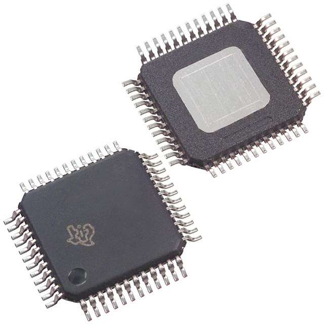


 工商网监
湘ICP备2023018690号
工商网监
湘ICP备2023018690号
