LM5176
SNVSAI1D – JUNE 2017 – REVISED AUGUST 2021
LM5176 55-V Wide VIN Synchronous 4-switch Buck-boost Controller
1 Features
3 Description
•
The LM5176 is a synchronous four-switch buck-boost
DC/DC controller capable of regulating the output
voltage at, above, or below the input voltage. The
LM5176 operates over a wide input voltage range of
4.2 V to 55 V (60-V absolute maximum) to support a
variety of applications.
•
•
•
•
•
•
•
•
•
•
•
•
•
•
Functional Safety-Capable
– Documentation available to aid functional safety
system design
Single inductor buck-boost controller for step-up/
step-down DC/DC conversion
Wide VIN: 4.2 V (2.5 V with bias) to 55 V (60 V
maximum)
Flexible VOUT: 0.8 V to 55 V
VOUT short protection
High efficiency buck-boost transition
Adjustable switching frequency
Optional frequency sync and dithering
Integrated 2-A MOSFET gate drivers
Cycle-by-cycle current limit and optional hiccup
Optional input or output average current limiting
Programmable input UVLO and soft start
Power Good and output overvoltage protection
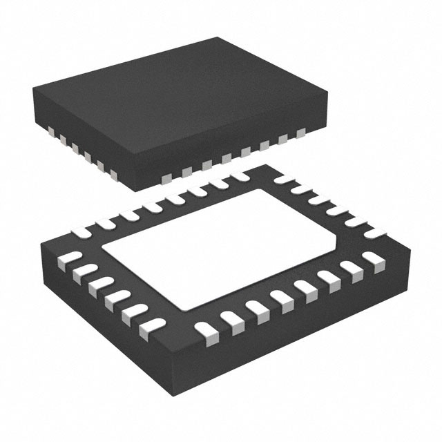
Available in HTSSOP-28 and QFN-28 packages
Create a custom design using the LM5176 with the
WEBENCH Power Designer
The LM5176 uses current-mode control both in
buck and boost modes of operation for superior
load and line regulation. The switching frequency
is programmed by an external resistor and can be
synchronized to an external clock signal.
The device also features a programmable soft-start
function and offers protection features including cycleby-cycle current limiting, input undervoltage lockout
(UVLO), output overvoltage protection (OVP), and
thermal shutdown. In addition, the LM5176 features
optional average input or output current limiting,
optional spread spectrum to reduce peak EMI, and
optional hiccup mode protection in sustained overload
conditions.
2 Applications
Device Information
Industrial PC power supplies
USB power delivery
Battery-powered systems
LED lighting
PART NUMBER
LM5176
PACKAGE
BODY SIZE
HTSSOP (28)
9.70 mm × 4.40 mm
QFN (28)
5.00 mm × 4.00 mm
VIN
Power Good
ISNS(-)
ISNS(+)
VISNS
EN/UVLO
VIN
VCC
Enable
VOUT
BOOT1
HDRV1
PGOOD
SW1
SS
LDRV1
SLOPE
CS
LM5176
RT/SYNC
CSG
LDRV2
COMP
SW2
AGND
BOOT2
PGND
VCC
BIAS
FB
VCC
MODE
HDRV2
DITH
•
•
•
•
VOSNS
Simplified Schematic
An IMPORTANT NOTICE at the end of this data sheet addresses availability, warranty, changes, use in safety-critical applications,
intellectual property matters and other important disclaimers. PRODUCTION DATA.
�LM5176
www.ti.com
SNVSAI1D – JUNE 2017 – REVISED AUGUST 2021
Table of Contents
1 Features............................................................................1
2 Applications..................................................................... 1
3 Description.......................................................................1
4 Revision History.............................................................. 2
5 Pin Configuration and Functions...................................3
6 Specifications.................................................................. 5
6.1 Absolute Maximum Ratings........................................ 5
6.2 ESD Ratings............................................................... 5
6.3 Recommended Operating Conditions.........................5
6.4 Thermal Information....................................................6
6.5 Electrical Characteristics.............................................6
6.6 Typical Characteristics................................................ 9
7 Detailed Description......................................................13
7.1 Overview................................................................... 13
7.2 Functional Block Diagram......................................... 14
7.3 Feature Description...................................................14
7.4 Device Functional Modes..........................................19
8 Application and Implementation.................................. 21
8.1 Application Information............................................. 21
8.2 Typical Application.................................................... 21
9 Power Supply Recommendations................................29
10 Layout...........................................................................30
10.1 Layout Guidelines................................................... 30
10.2 Layout Example...................................................... 31
11 Device and Documentation Support..........................32
11.1 Device Support........................................................32
11.2 Documentation Support.......................................... 32
11.3 Receiving Notification of Documentation Updates.. 32
11.4 Support Resources................................................. 32
11.5 Trademarks............................................................. 32
11.6 Electrostatic Discharge Caution.............................. 32
11.7 Glossary.................................................................. 33
12 Mechanical, Packaging, and Orderable
Information.................................................................... 33
4 Revision History
NOTE: Page numbers for previous revisions may differ from page numbers in the current version.
Changes from Revision C (June 2020) to Revision D (August 2021)
Page
• Updated the numbering format for tables, figures, and cross-references throughout the document. ................1
Changes from Revision B (June 2020) to Revision C (June 2020)
Page
• Added functional safety bullet to the Section 1 ..................................................................................................1
2
Submit Document Feedback
Copyright © 2021 Texas Instruments Incorporated
Product Folder Links: LM5176
�LM5176
www.ti.com
SNVSAI1D – JUNE 2017 – REVISED AUGUST 2021
VCC
SLOPE
7
22
PGND
SS
8
21
LDRV2
COMP
9
20
BOOT2
AGND
10
19
HDRV2
FB
11
18
SW2
VOSNS
12
17
PGOOD
ISNS(±)
13
16
CS
ISNS(+)
14
15
CSG
LM5176
HTSSOP-28
BOOT1
23
23
6
LDRV1
DITH
2
21
BIAS
RT
3
20
VCC
SLOPE
4
19
PGND
SS
5
18
LDRV2
COMP
6
17
BOOT2
AGND
7
16
HDRV2
FB
8
15
SW2
Figure 5-1. PWP Package 28-Pin HTSSOP With
PowerPAD™ Top View
14
RT
22
PGOOD
BIAS
HDRV1
24
24
5
1
13
DITH
MODE
CS
LDRV1
SW1
25
25
4
12
MODE
CSG
BOOT1
EN/UVLO
26
26
3
11
VISNS
ISNS(+)
HDRV1
VIN
27
27
2
10
VIN
ISNS(±)
SW1
VISNS
28
9
1
VOSNS
EN/UVLO
28
5 Pin Configuration and Functions
Figure 5-2. RHF Package 28-Pin QFN With
PowerPAD Top View
Table 5-1. Pin Functions
PIN
NAME
I/O
HTSSOP
QFN
EN/UVLO
1
26
I
VIN
2
27
I/P
VISNS
3
28
I
MODE
4
1
I
DESCRIPTION
Enable pin. For EN/UVLO < 0.4 V, the LM5176 is in a low current shutdown mode. For
EN/UVLO > 1.22 V, the PWM function is enabled, provided VCC exceeds the VCC UV
threshold.
The input supply pin to the IC. Connect VIN to a supply voltage between 4.2 V and 55 V.
VIN sense input. Connect to power stage input rail.
1.38 V < MODE < 2.22 V: CCM, hiccup enabled (set RMODE resistor to AGND = 93.1 kΩ)
2.6 V < MODE < VCC: CCM, hiccup disabled (set RMODE resistor to AGND = 200 kΩ or
connect to VCC)
DITH
5
2
I
A capacitor connected between the DITH pin and AGND is charged and discharged with a
current source. As the voltage on the DITH pin ramps up and down the oscillator frequency
is modulated by 10% of the nominal frequency set by the RT resistor. Grounding the DITH
pin will disable the dithering feature. In the external Sync mode, the DITH pin voltage is
ignored.
RT/SYNC
6
3
I
Switching frequency programming pin. An external resistor is connected to the RT/SYNC
pin and AGND to set the switching frequency. This pin can also be used to synchronize the
PWM controller to an external clock.
SLOPE
7
4
I
A capacitor connected between the SLOPE pin and AGND provides the slope
compensation ramp for stable current mode operation in both buck and boost mode.
SS
8
5
I
Soft-start programming pin. A capacitor between the SS pin and AGND pin programs
soft-start time.
COMP
9
6
O
Output of the error amplifier. An external RC network connected between COMP and
AGND compensates the regulator feedback loop.
AGND
10
7
G
Analog ground of the IC
FB
11
8
I
Feedback pin for output voltage regulation. Connect a resistor divider network from the
output of the converter to the FB pin.
Submit Document Feedback
Copyright © 2021 Texas Instruments Incorporated
Product Folder Links: LM5176
3
�LM5176
www.ti.com
SNVSAI1D – JUNE 2017 – REVISED AUGUST 2021
Table 5-1. Pin Functions (continued)
PIN
4
NAME
HTSSOP
QFN
VOSNS
12
9
I/O
DESCRIPTION
I
VOUT sense input. Connect to the power stage output rail.
ISNS(–)
ISNS(+)
13
14
10
11
I
Input or output current sense amplifier inputs. An optional current sense resistor connected
between ISNS(+) and ISNS(–) can be located either on the input side or on the output
side of the converter. If the sensed voltage across the ISNS(+) and ISNS(-) pins reaches
50 mV, a slow constant current (CC) control loop becomes active and starts discharging
the soft-start capacitor to regulate the drop across ISNS(+) and ISNS(–) to 50 mV. Short
ISNS(+) and ISNS(–) together to disable this feature.
CSG
15
12
I
The negative or ground input to the PWM current sense amplifier. Connect directly to the
low-side (ground) of the current sense resistor.
CS
16
13
I
The positive input to the PWM current sense amplifier
PGOOD
17
14
O
Power-Good open drain output. PGOOD is pulled low when FB is outside a -9%/+10%
regulation window around the 0.8-V VREF.
SW2
SW1
18
28
15
25
I
The boost and the buck side switching nodes, respectively.
HDRV2
HDRV1
19
27
16
24
O
Output of the high-side gate drivers. Connect directly to the gates of the high-side
MOSFETs.
BOOT2
BOOT1
20
26
17
23
P
An external capacitor is required between the BOOT1, BOOT2 pins and the SW1, SW2
pins respectively to provide bias to the high-side MOSFET gate drivers.
LDRV2
LDRV1
21
25
18
22
O
Output of the low-side gate drivers. Connect directly to the gates of the low-side
MOSFETs.
PGND
22
19
G
Power ground of the IC. The high current ground connection to the low-side gate drivers
VCC
23
20
I/O/P
BIAS
24
21
I/P
Optional input to the VCC bias regulator. Powering VCC from an external supply instead
of VIN can reduce power loss at high VIN. For VBIAS > 8 V, the VCC regulator draws power
from the BIAS pin.
PowerPAD™
—
—
—
Solder the PowerPAD to the analog ground. If possible, use thermal vias to connect to a
PCB ground plane for improved power dissipation.
Output of the VCC bias regulator. Connect capacitor to ground.
Submit Document Feedback
Copyright © 2021 Texas Instruments Incorporated
Product Folder Links: LM5176
�LM5176
www.ti.com
SNVSAI1D – JUNE 2017 – REVISED AUGUST 2021
6 Specifications
6.1 Absolute Maximum Ratings
(1)
MIN
MAX
VIN, EN/UVLO, VISNS, VOSNS, ISNS(+), ISNS(–)
–0.3
60
V
BIAS
–0.3
40
V
FB, SS, DITH, RT/SYNC, SLOPE, COMP
–0.3
3.6
V
SW1, SW2
UNIT
–1
60
V
SW1, SW2 (20 ns transient)
–5.0
65
V
VCC, MODE, PGOOD
–0.3
8.5
V
LDRV1, LDRV2
–0.3
8.5
V
BOOT1, HDRV1 with respect to SW1
–0.3
8.5
V
BOOT2, HDRV2 with respect to SW2
–0.3
8.5
V
BOOT1, BOOT2
–0.3
68
V
ISNS(+) with respect to ISNS(-)
-0.3
0.3
V
CS, CSG
–0.3
0.3
V
Operating junction temperature
–40
150
Storage temperature, Tstg
–65
150
(1)
°C
Stresses beyond those listed under Absolute Maximum Ratings may cause permanent damage to the device. These are stress
ratings only, which do not imply functional operation of the device at these or any other conditions beyond those indicated under
Recommended Operating Conditions. Exposure to absolute-maximum-rated conditions for extended periods may affect device
reliability.
6.2 ESD Ratings
VALUE
VESD (1)
(1)
(2)
(3)
Human body model (HBM) ESD stress
voltage(2)
±2000
Charged device model (CDM) ESD stress voltage(3)
±750
UNIT
V
Electrostatic discharge (ESD) to measure device sensitivity and immunity to damage caused by assembly line electrostatic discharges
into the device.
Level listed above is the passing level per ANSI/ESDA/JEDEC JS-001. JEDEC document JEP155 states that 500 V HBM allows safe
manufacturing with a standard ESD control process.
Level listed above is the passing level per EIA-JEDEC JESD22-C101. JEDEC document JEP157 states that 250 V CDM allows safe
manufacturing with a standard ESD control process.
6.3 Recommended Operating Conditions
over operating free-air temperature range (unless otherwise noted)(1)
MIN
MAX
UNIT
VIN
Input bias voltage
4.2
55
VISNS
Input power stage voltage with external bias (BIAS ≥ 5 V or VIN ≥
4.5 V)
2.5
55
BIAS
Bias supply voltage (when VCC in regulation)
8
36
V
VOSNS
Output voltage range
0.8
55
V
EN/UVLO
Enable voltage range
0
55
V
ISNS(+), ISNS(–)
Average current sense common mode range
0
55
V
TJ
Operating temperature(2)
–40
125
°C
fsw
Operating frequency
100
600
kHz
(1)
(2)
V
V
Recommended Operating Conditions are conditions under the device is intended to be functional. For specifications and test
conditions, see Section 6.5.
High junction temperatures degrade operating lifetimes. Operating lifetime is de-rated for junction temperatures greater than 125°C.
Submit Document Feedback
Copyright © 2021 Texas Instruments Incorporated
Product Folder Links: LM5176
5
�LM5176
www.ti.com
SNVSAI1D – JUNE 2017 – REVISED AUGUST 2021
6.4 Thermal Information
LM5176
THERMAL
METRIC(1)
PWP (HTSSOP)
RHF (QFN)
UNIT
28 PINS
RθJA
Junction-to-ambient thermal resistance
32.6
34.7
°C/W
RθJC(top)
Junction-to-case (top) thermal resistance
21.4
26.6
°C/W
RθJB
Junction-to-board thermal resistance
8.2
6.3
°C/W
ψJT
Junction-to-top characterization parameter
0.3
0.3
°C/W
ψJB
Junction-to-board characterization parameter
8.3
6.2
°C/W
RθJC(bot)
Junction-to-case (bottom) thermal resistance
1
2.0
°C/W
(1)
For more information about traditional and new thermal metrics, see the Semiconductor and IC Package Thermal Metrics application
report.
6.5 Electrical Characteristics
Typical values correspond to TJ = 25°C. Minimum and maximum limits apply over the –40°C to 125°C junction temperature
range unless otherwise stated. VIN = 24 V unless otherwise stated.(1)
PARAMETER
TEST CONDITION
MIN
TYP
MAX
UNIT
2.6
10
µA
2
4
mA
SUPPLY VOLTAGE (VIN)
IQ
VIN shutdown current
VEN/UVLO = 0 V
VIN operating current
VEN/UVLO = 2 V, VFB = 0.9 V
VVCC(VIN)
Regulation voltage
VBIAS = 0 V, VCC open
6.95
7.35
7.88
V
VUV(VCC)
VCC undervoltage lockout
VCC increasing
3.11
3.27
3.43
V
VCC
Undervoltage hysteresis
176
IVCC
VCC current limit
VVCC = 0 V
ROUT(VCC)
VCC regulator output impedance
IVCC = 30 mA, VIN = 4 V
BIAS switchover voltage
VIN = 24 V
VEN(STBY)
Standby threshold
EN/UVLO rising
IEN(STBY)
Standby source current
VEN/UVLO = 1.1 V
VEN(OP)
Operating threshold
ΔIHYS(OP)
Operating hysteresis current
ISS
mV
65
mA
8
16
Ω
7.25
8
8.75
V
0.55
0.82
0.97
V
1
2
3
µA
EN/UVLO rising
1.17
1.22
1.29
V
VEN/UVLO = 1.5 V
2.15
3.15
4.25
µA
Soft-start pullup current
VSS = 0 V
3.75
5
6.35
µA
VSS(CL)
SS clamp voltage
SS open
1.21
V
VFB - VSS
FB to SS offset
VSS = 0 V
–18
mV
BIAS
VBIAS(SW)
EN/UVLO
SS
EA (ERROR AMPLIFIER)
VREF
Feedback reference voltage
FB = COMP
0.788
gmEA
Error amplifier gm
ISINK/ISOURCE
COMP sink/source current
ROUT
Amplifier output resistance
BW
Unity gain bandwidth
IBIAS(FB)
Feedback pin input bias current
FB in regulation
fSW(1)
Switching frequency 1
RT = 40 kΩ
175
200
225
fSW(2)
Switching frequency 2
RT = 20 kΩ
350
390
430
VFB=VREF ± 300 mV
0.800
0.812
V
1.31
mS
280
µA
20
MΩ
2
MHz
25
nA
FREQUENCY
6
Submit Document Feedback
kHz
Copyright © 2021 Texas Instruments Incorporated
Product Folder Links: LM5176
�LM5176
www.ti.com
SNVSAI1D – JUNE 2017 – REVISED AUGUST 2021
Typical values correspond to TJ = 25°C. Minimum and maximum limits apply over the –40°C to 125°C junction temperature
range unless otherwise stated. VIN = 24 V unless otherwise stated.(1)
PARAMETER
TEST CONDITION
MIN
TYP
MAX
UNIT
DITHER
IDITHER
Dither source/sink current
11
VDITHER
Dither high threshold
1.27
Dither low threshold
1.16
µA
V
SYNC
VSYNC
Sync input high threshold
2.1
Sync input low threshold
PWSYNC
1.2
Minimum sync input pulse width
50
V
ns
CURRENT LIMIT
VCS(BUCK)
VCS(BOOST)
IBIAS(CS/CSG)
Buck current limit threshold (Valley,
HTSSOP-28)
VIN = VVISNS = 24 V, VVOSNS = 12 V,
VSLOPE = 0 V
66
80
94
Buck current limit threshold (Valley,
QFN-28)
VIN = VVISNS = 24 V, VVOSNS = 12 V,
VSLOPE = 0 V
60
80
94
Boost current limit threshold (Peak,
HTSSOP-28)
VIN = VVISNS = 12 V, VVOSNS = 18 V,
VSLOPE = 0 V
100
120
140
Boost current limit threshold (Peak,
QFN-28)
VIN = VVISNS = 12 V, VVOSNS = 18 V,
VSLOPE = 0 V
96
120
140
CS/CSG pin bias current
VCS = VCSG = 0 V
IOFFSET(CS/CSG) CSG pin bias current
-80
VCS = VCSG = 0 V
19
mV
mV
mV
mV
µA
CONSTANT CURRENT LOOP
VSNS
Average current loop regulation target
VISNS(-) = 24 V, sweep ISNS(+), VSS =
0.8 V
ISNS
ISNS(+), ISNS(–) pin bias currents
VISNS(+) = VISNS(–) = VIN = 24 V
3
µA
Gm
gm of soft-start pulldown amplifier
VISNS(+)–VISNS(–) = 55 mV, VSS = 0.5
V
1
mS
Buck adaptive slope current
VIN = VVISNS = 24 V, VVOSNS = 12 V,
VSLOPE = 0 V
24
30
35
µA
Boost adaptive slope current
VIN = VVISNS = 12 V, VVOSNS = 18 V,
VSLOPE = 0 V
13
17
21
µA
43
50
57
mV
SLOPE
ISLOPE
gmSLOPE
Slope compensation amplifier gm
2
µS
MODE
IMODE
Source current out of MODE pin
17
20
23
µA
VCCM_HIC
CCM with hiccup threshold
1.18
1.28
1.38
V
VCCM
CCM no hiccup threshold
2.22
2.4
2.6
V
Submit Document Feedback
Copyright © 2021 Texas Instruments Incorporated
Product Folder Links: LM5176
7
�LM5176
www.ti.com
SNVSAI1D – JUNE 2017 – REVISED AUGUST 2021
Typical values correspond to TJ = 25°C. Minimum and maximum limits apply over the –40°C to 125°C junction temperature
range unless otherwise stated. VIN = 24 V unless otherwise stated.(1)
PARAMETER
TEST CONDITION
MIN
TYP
MAX
UNIT
PGOOD
VPGD
PGOOD trip threshold for falling FB
Measured with respect to VREF
PGOOD trip threshold for rising FB
Measured with respect to VREF
–9%
10%
Hysteresis
2.5%
ILEAK(PGD)
PGOOD leakage current
ISINK(PGD)
PGOOD sink current
VPGOOD = 0.4 V
Output overvoltage threshold at FB pin
Measured with respect to VREF
2
4.2
100
nA
6.5
mA
OUTPUT OVP
VOVP
Hysteresis
10%
2.5%
NMOS DRIVERS
IHDRV1,2
ILDRV1,2
Driver peak source current
VBOOT - VSW = 7 V
1.8
A
Driver peak sink current
VBOOT - VSW = 7 V
2.2
A
Driver peak source current
1.8
A
Driver peak sink current
2.2
A
Driver pullup resistance
VBOOT - VSW = 7 V
1.8
Ω
Driver pulldown resistance
VBOOT - VSW = 7 V
1.1
Ω
BOOT1,2 to SW1,2 UVLO threshold
HDRV1,2 shut off
3.4
V
BOOT1,2 to SW1,2 UVLO hysteresis
HDRV1,2 start switching
150
mV
Driver pullup resistance
1.7
Ω
Driver pulldown resistance
1.3
Ω
tDT1
Dead time HDRV1,2 off to LDRV1,2 on
45
ns
tDT2
Dead time LDRV1,2 off to HDRV1,2 on
45
ns
165
°C
15
°C
RHDRV1,2
VUV(BOOT1,2)
RLDRV1,2
THERMAL SHUTDOWN
TSD
Thermal shutdown temperature
TSD(HYS)
Thermal shutdown hysteresis
(1)
8
All minimum and maximum limits are specified by correlating the electrical characteristics to process and temperature variations and
applying statistical process control.
Submit Document Feedback
Copyright © 2021 Texas Instruments Incorporated
Product Folder Links: LM5176
�LM5176
www.ti.com
SNVSAI1D – JUNE 2017 – REVISED AUGUST 2021
6.6 Typical Characteristics
At TA = 25°C, unless otherwise stated.
99
100
96
EFFICIENCY (%)
EFFICIENCY (%)
98
97
96
95
92
88
84
94
VIN = 9V
VIN = 12V
VIN = 24V
80
93
5
10
15
20
VOUT = 12 V
IOUT = 5 A
25
30
VIN (V)
35
40
45
0
50
1
2
3
4
LOAD CURRENT (A)
D009
fsw = 300 kHz
VOUT = 12 V
L1 = 4.7 μH
5
6
D008
fsw = 300 kHz
L1 = 4.7 μH
Figure 6-2. Efficiency vs Load
Figure 6-1. Efficiency vs VIN
8
600
6
400
VCC (V)
FREQUENCY (kHz)
500
300
4
200
2
100
0
10
20
30
40
50
60
RT (k:)
70
80
90
0
100
0
2
4
D004
Figure 6-3. Oscillator Frequency
6
VIN (V)
8
10
12
D002
Figure 6-4. VCC vs VIN
3.0
3.0
2.5
2.6
IIN (PA)
IIN (mA)
2.0
2.2
1.8
1.5
1.0
1.4
-40 qC
25 qC
125 qC
0.5
BIAS = 0V
BIAS = 12V
1.0
0.0
0
10
20
30
VIN (V)
40
50
60
0
10
D007
Figure 6-5. IIN Operating vs VIN
20
30
VIN (V)
40
50
60
D010
Figure 6-6. IIN Shutdown vs VIN
Submit Document Feedback
Copyright © 2021 Texas Instruments Incorporated
Product Folder Links: LM5176
9
�LM5176
www.ti.com
SNVSAI1D – JUNE 2017 – REVISED AUGUST 2021
110
BUCK CURRENT LIMIT (mV)
1.30
VEN/UVLO (V)
1.26
1.22
1.18
1.14
1.10
-40
-20
0
20
40
60
80
TEMPERATURE (qC)
100
120
140
100
90
80
70
60
50
-40
-20
0
D013
Figure 6-7. ENABLE/UVLO Rising Threshold vs
Temperature
20
40
60
80
TEMPERATURE (qC)
100
120
140
D014
Figure 6-8. Buck Current Limit vs Temperature
BOOST CURRENT LIMIT (mV)
150
140
SW1
130
SW2
120
110
IL1
100
90
-40
-20
0
20
40
60
80
TEMPERATURE (qC)
100
120
140
SW1
SW2
SW2
IL1
IL1
VIN = 11 V
VOUT = 12 V
Figure 6-11. Forced CCM Operation (Buck-Boost)
VIN = 6 V
Figure 6-10. Forced CCM Operation (Boost)
SW1
VOUT = 12 V
10
VOUT = 12 V
D015
Figure 6-9. Boost Current Limit vs Temperature
VIN = 12 V
Figure 6-12. Forced CCM Operation (Buck-Boost)
Submit Document Feedback
Copyright © 2021 Texas Instruments Incorporated
Product Folder Links: LM5176
�LM5176
www.ti.com
SNVSAI1D – JUNE 2017 – REVISED AUGUST 2021
SW1
SW1
SW2
SW2
IL1
IL1
VOUT = 12 V
VIN = 13 V
VOUT = 12 V
Figure 6-13. Forced CCM Operation (Buck-Boost)
VIN = 24 V
Figure 6-14. Forced CCM Operation (Buck)
VOUT
500 mV/div
VOUT
500 mV/div
IOUT
2 A/div
IOUT
2 A/div
500 µs/div
500 µs/div
VOUT = 6 V
VIN = 11 V
Load 3 A to 6 A
Figure 6-15. Load Step (Boost)
VOUT
500 mV/div
VIN = 12 V
Load 3 A to 6 A
Figure 6-16. Load Step (Buck-Boost)
VIN
10 V/div
VOUT
1 V/div
IOUT
2 A/div
500 µs/div
VOUT = 24 V
VOUT = 12 V
VIN = 12 V
Load 3 A to 6 A
IL
5 A/div
VIN = 8 V to 24 V
Figure 6-17. Load Step (Buck)
1 ms/div
VOUT = 12 V
IOUT = 3 A
Figure 6-18. Line Transient
Submit Document Feedback
Copyright © 2021 Texas Instruments Incorporated
Product Folder Links: LM5176
11
�LM5176
www.ti.com
SNVSAI1D – JUNE 2017 – REVISED AUGUST 2021
12
VOUT (V)
VOUT
5 V/div
15
Overload
released
9
6
3
IL
5 A/div
VIN = 24 V
20 ms/div
VOUT = 12 V
0
1
Hiccup Enabled
Figure 6-19. Hiccup Mode Current Limit
12
0
VIN = 24 V
2
3
IOUT (A)
4
5
6
D021
RSNS = 10 mΩ
Figure 6-20. Constant Current Constant Voltage
(CCCV) Operation
Submit Document Feedback
Copyright © 2021 Texas Instruments Incorporated
Product Folder Links: LM5176
�LM5176
www.ti.com
SNVSAI1D – JUNE 2017 – REVISED AUGUST 2021
7 Detailed Description
7.1 Overview
The LM5176 is a wide input voltage four-switch buck-boost controller IC with integrated drivers for N-channel
MOSFETs. It operates in buck mode when VIN is greater than VOUT and in boost mode when VIN is less than
VOUT. When V IN is close to VOUT, the device operates in a proprietary transition buck or boost mode. The control
scheme provides smooth operation for any input/output combination within the specified operating range. The
buck or boost transition control scheme provides a low ripple output voltage when VIN equals VOUT without
compromising the efficiency.
The LM5176 integrates four N-Channel MOSFET drivers including two low-side drivers and two high-side
drivers, eliminating the need for external drivers or floating bias supplies. The internal VCC regulator supplies
internal bias rails as well as the MOSFET gate drivers. The VCC regulator is powered either from the input
voltage through the VIN pin or from the output or an external supply through the BIAS pin for improved efficiency.
The PWM control scheme is based on valley current mode control for buck operation and peak current mode
control for boost operation. The inductor current is sensed through a single sense resistor in series with the
low-side MOSFETs. The sensed current is also monitored for cycle-by-cycle current limit. The behavior of the
LM5176 during an overload condition is dependent on the MODE pin programming (see the Section 7.4.2
section). If hiccup mode fault protection is selected, the controller turns off after a fixed number of switching
cycles in cycle-by-cycle current limit and restarts after another fixed number of clock cycles. The hiccup mode
reduces the heating in the power components in a sustained overload condition. If hiccup mode is disabled
through the MODE pin, the controller remains in a cycle-by-cycle current limit condition until the overload is
removed.
In addition to the cycle-by-cycle current limiting, the LM5176 also provides an optional average current regulation
loop that can be configured for either input or output current limiting. This is useful for battery charging or other
applications where a constant current behavior may be required.
The soft-start time of LM5176 is programmed by a capacitor connected to the SS pin to minimize the inrush
current and overshoot during start-up.
The precision EN/UVLO pin supports programmable input undervoltage lockout (UVLO) with hysteresis. The
output overvoltage protection (OVP) feature turns off the high-side drivers when the voltage at the FB pin
exceeds the output overvoltage threshold (VOVP). The PGOOD output indicates when the FB voltage is inside
the PGOOD regulation window centered at VREF.
Submit Document Feedback
Copyright © 2021 Texas Instruments Incorporated
Product Folder Links: LM5176
13
�LM5176
www.ti.com
SNVSAI1D – JUNE 2017 – REVISED AUGUST 2021
7.2 Functional Block Diagram
BIAS
VIN
¨,HYS(OP)
+
-
EN/UVLO
VEN(OP)
VCC
OPERATING
EN & BIAS
LOGIC
IEN(STBY)
+
-
VEN(STBY)
THERMAL
SHUTDOWN
STANDBY
45 mV
1.2 V
PGOOD
+
1.1VREF
OV
VOVP
FB
+
+
ISS
-
SS
+
ISNS(+)
-
ISNS(-)
+
1 mA/V
0.91VREF
CONSTANT
CURRENT LOOP
3.3V
SS
FB
VREF
GM ERROR
AMPLIFIER
+
+
BOOT1
PWM
COMPARATOR
1.6V
HDRV1
+
-
-
SW1
VCC
LDRV1
COMP
CS AMPLIFIER
CS
CLK
BOOT2
+
ACS=5
CSG
BUCK-BOOST CONTROLLER
LOGIC
HDRV2
ILIMIT
COMPARATOR
-
SW2
+
-
VCC
LDRV2
VISNS
VILIM
SLOPE COMP
VOSNS
SLOPE
HICCUP CURRENT
LIMIT
RT/SYNC
OSC/SYNC
MODE
CLK
DITH
AGND
PGND
7.3 Feature Description
7.3.1 Fixed Frequency Valley/Peak Current Mode Control with Slope Compensation
The LM5176 implements a fixed frequency current mode control of both the buck and boost switches. The
output voltage, scaled down by the feedback resistor divider, appears at the FB pin and is compared to the
internal reference (VREF) by an internal error amplifier. The error amplifier produces an error voltage by driving
the COMP pin. An adaptive slope compensation signal based on VIN, VOUT, and the capacitor at the SLOPE
pin is added to the current sense signal measured across the CS and CSG pins. The result is compared to the
COMP error voltage by the PWM comparator.
The LM5176 regulates the output using valley current mode control in buck mode and peak current mode control
in boost mode. For valley current mode control, the high-side buck MOSFET controlled by HDRV1 is turned on
by the PWM comparator at the valley of the inductor ripple current and turned off by the oscillator clock signal.
Valley current mode control is advantageous for buck converters where the PWM controller must resolve very
short on-times. For peak current mode control in the boost mode, the low-side boost MOSFET controlled by
14
Submit Document Feedback
Copyright © 2021 Texas Instruments Incorporated
Product Folder Links: LM5176
�LM5176
www.ti.com
SNVSAI1D – JUNE 2017 – REVISED AUGUST 2021
LDRV2 is turned on by the clock signal in each switching cycle and turned off by the PWM comparator at the
peak of the inductor ripple current.
The low-side gate drive, LDRV1, complementary to the HDRV1 drive signal, controls the synchronous
rectification MOSFET of the buck stage. The high-side gate drive, HDRV2, complementary to the low-side gate
drive LDRV2, controls the high-side synchronous rectifier of the boost stage. For operation with VIN close to
VOUT, the LM5176 uses a proprietary buck or boost transition scheme to achieve smooth, low ripple transition
zone behavior.
Peak and valley current mode controllers require slope compensation for stable current loop operation at duty
cycle greater than 50% in peak current mode control and less than 50% in valley current mode control. The
LM5176 provides a SLOPE pin to program optimum slope for any VIN and VOUT combination using an external
capacitor.
7.3.2 VCC Regulator and Optional BIAS Input
The VCC regulator provides a regulated bias supply to the gate drivers. When EN/UVLO is above the standby
threshold (VEN(STBY)), the VCC regulator is turned on. For VIN less than the VCC regulation target, the VCC
voltage tracks V IN with a small voltage drop as shown in Figure 6-4. If the EN/UVLO input is above the operating
threshold (VEN(OP)) and VCC exceeds the VCC UV threshold (VUV(VCC)), the controller is enabled and switching
begins.
The VCC regulator draws power from VIN when there is no supply voltage connected to the BIAS pin. If the BIAS
pin is connected to an external voltage source that exceeds VCC by one diode drop, the VCC regulator draws
power from the BIAS input instead of VIN. Connecting the BIAS pin to VOUT in applications with VOUT greater
than 8.5 V improves the efficiency of the regulator in the buck mode.
For low VIN operation, ensure that the VCC voltage is sufficient to fully enhance the MOSFETs. Use an external
bias supply if VIN dips below the voltage required to sustain the VCC voltage. For these conditions, use a series
blocking diode between the input supply and the VIN pin (Figure 7-1). This prevents VCC from back-feeding into
VIN through the body diode of the VCC regulator.
A ceramic capacitor of 16 V or higher voltage rating and a value between 1 µF and 4.7 µF is required to supply
the VCC regulator load transients. The VCC bypass capacitor should be connected between VCC and PGND
pins.
Series Blocking Diode
VIN
VIN
CVIN
LM5176
Optional
Bias Supply/ VOUT
BIAS
VCC
CBIAS
CVCC
Figure 7-1. VCC Regulator and Optional BIAS
7.3.3 Enable/UVLO
The LM5176 has a dual function enable and undervoltage lockout (UVLO) circuit. The EN/UVLO pin has three
distinct voltage ranges: shutdown, standby, and operating (see Section 7.4.1). When the EN/UVLO pin is below
the standby threshold, VEN(STBY), the converter is held in a low power shutdown mode. When EN/UVLO voltage
is greater than the standby threshold, VEN(STBY), but less than the operating threshold, VEN(OP), the internal
bias rails and the VCC regulator are enabled but the soft-start (SS) pin is held low and the PWM controller is
disabled. A pullup current IEN(STBY) is sourced out of the EN/UVLO pin in standby mode to provide hysteresis
Submit Document Feedback
Copyright © 2021 Texas Instruments Incorporated
Product Folder Links: LM5176
15
�LM5176
www.ti.com
SNVSAI1D – JUNE 2017 – REVISED AUGUST 2021
between the shutdown mode and the standby mode. When EN/UVLO is greater than the operating threshold,
VEN(OP), and VCC is above the undervoltage threshold, VUV(VCC), the controller starts operation. A hysteresis
current ΔIHYS(OP) is sourced out of the EN/UVLO pin when the EN/UVLO input exceeds the operating threshold
to provide hysteresis that prevents on/off chattering in the presence of noise with a slowly changing input
voltage.
The VIN UVLO threshold is typically set by a resistor divider from VIN to AGND (Figure 7-2). The turnon threshold
VIN(UV) is calculated using Equation 1 where RUV2 is the upper resistor and RUV1 is the lower resistor in the
EN/UVLO resistor divider:
VIN(UV)
§ RUV2 ·
VEN(OP) u ¨ 1
¸ RUV2 u IEN(STBY)
RUV1 ¹
©
(1)
The hysteresis between the UVLO turnon threshold and turnoff threshold is set by the upper resistor in the
EN/UVLO resistor divider and is given by:
'VHYS(UV)
'IHYS(OP) u RUV2
(2)
VIN
LM5176
RUV2
EN/UVLO
RUV1
Figure 7-2. UVLO Threshold Programming
7.3.4 Soft Start
The LM5176 soft-start time is programmed using a soft-start capacitor from the SS pin to AGND. When the
converter is enabled, an internal current source (ISS) charges the soft-start capacitor. When the SS pin voltage
is below the feedback reference voltage, VREF, the soft-start pin controls the regulated FB voltage. Once SS
exceeds VREF, the soft-start interval is complete and the error amplifier is referenced to VREF. The soft-start time
is given by Equation 3:
t ss
CSS u VREF
ISS
(3)
The soft-start capacitor is internally discharged when the converter is disabled because of EN/UVLO falling
below the operating threshold or VCC falling below the VCC UV threshold. The soft-start pin is also discharged
when the converter is in hiccup mode current limiting or in thermal shutdown. When average input or output
current limiting is active, the soft-start capacitor is discharged by the constant current loop transconductance
(gm) amplifier to limit either input or output current.
7.3.5 Overcurrent Protection
The LM5176 provides cycle-by-cycle current limit to protect against overcurrent and short circuit conditions. In
buck operation, the sensed valley voltage across the CSG and CS pins is limited to VCS(BUCK). The high-side
buck switch skips a cycle if the sensed voltage does not fall below this threshold during the buck switch off time.
In boost operation, the maximum peak voltage across CS and CSG is limited to VCS(BOOST). If the peak current
in the low-side boost switch causes the voltage across CS and CSG to exceed this threshold voltage, the boost
switch is turned off for the remainder of the clock cycle.
16
Submit Document Feedback
Copyright © 2021 Texas Instruments Incorporated
Product Folder Links: LM5176
�LM5176
www.ti.com
SNVSAI1D – JUNE 2017 – REVISED AUGUST 2021
Applying the appropriate voltage to the MODE pin of the LM5176 enables hiccup mode fault protection (see
Section 7.4.2). In hiccup mode, the controller shuts down after detecting cycle-by-cycle current limiting for 128
consecutive cycles and the soft-start capacitor is discharged. The soft-start capacitor is automatically released
after 4000 oscillator clock cycles and the controller restarts. If hiccup mode protection is not enabled through the
MODE pin, the LM5176 will operate in cycle-by-cycle current limiting as long as the overload condition persists.
7.3.6 Average Input/Output Current Limiting
The LM5176 provides optional average current limiting capability to limit either the input or the output current of
the DC/DC converter. The average current limiting circuit uses an additional current sense resistor connected in
series with the input supply or output voltage of the converter. A current sense gm amplifier with inputs at the
ISNS(+) and ISNS(-) pins monitors the voltage across the sense resistor and compares it with an internal 50-mV
reference. If the drop across the sense resistor is greater than 50 mV, the gm amplifier gradually discharges
the soft-start capacitor. When the soft-start capacitor discharges below the feedback reference voltage, VREF,
the output voltage of the converter decreases to limit the input or output current. The average current limiting
feature can be used in applications requiring a regulated current from the input supply or into the load. The target
constant current is given by Equation 4:
ICL(AVG)
50 mV
RSNS
(4)
A filter network as shown in Figure 8-1 is often used across the ISNS(+) and ISNS(-) pins to filter the ripple in the
average current sense signal.
The average current loop can be disabled by shorting the ISNS(+) and ISNS(-) pins together to AGND.
7.3.7 Operation Above 40-V Input
For application where input voltage is higher than 40 V, a 2-kΩ resistor in series with the VISNS pin is required
as shown in Figure 8-1.
7.3.8 CCM Operation
The LM5176 works in continuous conduction mode (CCM). In CCM operation, the inductor current can flow
in either direction and the controller switches at a fixed frequency regardless of the load current. The CCM
operation is useful for noise-sensitive applications where a fixed switching eases filter design.
7.3.9 Frequency and Synchronization (RT/SYNC)
The LM5176 switching frequency can be programmed between 100 kHz and 600 kHz using a resistor from the
RT/SYNC pin to AGND. The RT resistor is related to the nominal switching frequency (Fsw) by Equation 5:
RT
§ 1 ·
¨
¸ 190 ns
© Fsw ¹
116 pF
(5)
Figure 6-3 in the Section 6.6 shows the relationship between the programmed switching frequency (Fsw) and the
RT resistor.
The RT/SYNC pin can also be used to synchronize the internal oscillator to an external clock signal. The
external synchronization pulse is ac coupled using a capacitor to the RT/SYNC pin. The external synchronization
pulse frequency range is 75% to 125% of the resistor programmed frequency. A 50% duty cycle is acceptable for
external SYNC.
Submit Document Feedback
Copyright © 2021 Texas Instruments Incorporated
Product Folder Links: LM5176
17
�LM5176
www.ti.com
SNVSAI1D – JUNE 2017 – REVISED AUGUST 2021
LM5176
RT/SYNC
external SYNC
CSYNC
RT
Figure 7-3. Using External SYNC
7.3.10 Frequency Dithering
The LM5176 provides an optional frequency dithering function that is enabled by connecting a capacitor from
DITH to AGND. Figure 7-4 illustrates the dithering circuit. A triangular waveform centered at 1.22 V is generated
across the CDITH capacitor. This triangular waveform modulates the oscillator frequency by 10% of the nominal
frequency set by the RT resistor. The CDITH capacitance value sets the rate of the low frequency modulation. A
lower CDITH capacitance will modulate the oscillator frequency at a faster rate than a higher capacitance. For
the dithering circuit to effectively reduce peak EMI, the modulation rate must be much less than the oscillator
frequency (Fsw). Equation 6 calculates the DITH pin capacitance required to set the modulation frequency, FMOD.
Connecting the DITH pin directly to AGND disables frequency dithering, and the internal oscillator operates at a
fixed frequency set by the RT resistor. Dither is disabled when external SYNC is used.
CDITH
10 PA
FMOD u 0.24 V
(6)
1.22 V + 5%
LM5176
1.22 V
1.22 V - 5 %
DITH
CDITH
Figure 7-4. Dither Operation
7.3.11 Output Overvoltage Protection (OVP)
The LM5176 provides an output overvoltage protection (OVP) circuit that turns off the gate drives when the
feedback voltage is above the output overvoltage threshold VOVP. Switching resumes once the feedback voltage
falls below the OVP threshold. There is a small hysteresis to prevent chattering.
7.3.12 Power Good (PGOOD)
PGOOD is an open-drain output that is pulled low when the voltage at the FB pin is outside -9%/+10% of the
nominal VREF. The PGOOD internal N-Channel MOSFET pulldown strength is typically 4.2 mA. This pin can be
connected to a voltage supply of up to 8 V through a pullup resistor.
7.3.13 Gm Error Amplifier
The LM5176 has a gm error amplifier for loop compensation. The gm amplifier output (COMP) range is 0.3 V
to 3 V. Connect an Rc1-Cc1 compensation network between COMP and ground for type II (PI) compensation
(see Figure 8-1). Another pole is usually added using Cc2 to suppress higher frequency noise and switching
frequency ripple.
18
Submit Document Feedback
Copyright © 2021 Texas Instruments Incorporated
Product Folder Links: LM5176
�LM5176
www.ti.com
SNVSAI1D – JUNE 2017 – REVISED AUGUST 2021
The COMP output voltage (VCOMP) range limits the possible VIN and IOUT ranges for a given design. In buck
mode, the maximum VIN for which the converter can regulate the output at no load is when VCOMP reaches 0.3 V.
Equation 7 gives VCOMP as a function of VIN at no load in CCM buck mode:
VCOMP(BUCK)
1.6 V ACS ˜ RSENSE ˜
VOUT
˜ 1 DBUCK
2 ˜ L1˜ Fsw
2 PS ˜ VIN
VOUT
6 PA
CSLOPE ˜ Fsw
˜ 1 DBUCK
(7)
Where DBUCK in Equation 7 is the buck duty cycle given by:
DBUCK
VOUT
VIN
(8)
A larger L1, lower slope ripple (higher CSLOPE), smaller sense resistor (RSENSE), and higher frequency can
increase the maximum VIN range for buck operation.
For boost mode, the minimum VIN for which the converter can regulate the output at full load is when VCOMP
reaches 3 V. Equation 9 gives VCOMP as a function of VIN in boost mode:
VCOMP(BOOST)
1.6 V
§
V
ACS ˜ RSENSE ˜ ¨ IOUT ˜ OUT
VIN
©
·
VIN
˜ DBOOST ¸
2 ˜ L1˜ Fsw
¹
2 PS ˜ VOUT
VIN
CSLOPE ˜ Fsw
5 PA
˜ DBOOST
(9)
Where DBOOST in Equation 9 is the boost duty cycle given by:
DBOOST
1
VIN
VOUT
(10)
A larger L1, lower slope ripple (higher CSLOPE), smaller sense resistor (RSENSE), and higher frequency can
extend the minimum VIN range for boost operation.
7.3.14 Integrated Gate Drivers
The LM5176 provides four N-channel MOSFET gate drivers: two floating high-side gate drivers at the HDRV1
and HDRV2 pins, and two ground referenced low-side drivers at the LDRV1 and LDRV2 pins. Each driver is
capable of sourcing 1.8-A and sinking 2.2-A peak current. In buck operation, LDRV1 and HDRV1 are switched
by the PWM controller while HDRV2 remains continuously on. In boost operation, LDRV2 and HDRV2 are
switched while HDRV1 remains continuously on.
The low-side gate drivers are powered from VCC and the high-side gate drivers HDRV1 and HDRV2 are
powered from bootstrap capacitors CBOOT1 (between BOOT1 and SW1) and CBOOT2 (between BOOT2 and
SW2), respectively. The CBOOT1 and CBOOT2 capacitors are charged through external Schottky diodes connected
to the VCC pin as shown in Figure 8-1.
In most applications, ceramic capacitors of 16-V or higher voltage rating and values between 0.1 µF and 0.22 µF
are sufficient for CBOOT1 and CBOOT2.
7.3.15 Thermal Shutdown
The LM5176 is protected by a thermal shutdown circuit that shuts down the device when the internal junction
temperature exceeds 165°C (typical). The soft-start capacitor is discharged when thermal shutdown is triggered
and the gate drivers are disabled. The converter automatically restarts when the junction temperature drops by
the thermal shutdown hysteresis of 15°C below the thermal shutdown threshold.
7.4 Device Functional Modes
Refer to Section 7.3.3 for the description of EN/UVLO pin function. Section 7.4.1 lists the shutdown, standby,
and operating modes for LM5176 as a function of EN/UVLO and VCC voltages.
Submit Document Feedback
Copyright © 2021 Texas Instruments Incorporated
Product Folder Links: LM5176
19
�LM5176
www.ti.com
SNVSAI1D – JUNE 2017 – REVISED AUGUST 2021
7.4.1 Shutdown, Standby, and Operating Modes
EN/UVLO
VCC
DEVICE MODE
EN/UVLO < VEN(STBY)
—
Shutdown: VCC off, No switching
VEN(STBY) < EN/UVLO < VEN(OP) —
Standby: VCC on, No switching
EN/UVLO > VEN(OP)
VCC < VUV(VCC)
Standby: VCC on, No switching
EN/UVLO > VEN(OP)
VCC > VUV(VCC)
Operating: VCC on, Switching enabled
7.4.2 MODE Pin Configuration
The MODE pin is used to select hiccup mode current limit. The MODE selection is based on the voltages at the
MODE pin. The MODE voltage is decided by the programming resistor, RMODE, between MODE and AGND, and
the source current out of the MODE pin (IMODE). MODE is latched during start-up.
20
MODE PIN CONNECTION
HICCUP FAULT PROTECTION
RMODE to AGND = 200 kΩ or connect
MODE to VCC
No Hiccup
RMODE to AGND = 93.1 kΩ
Hiccup Enabled
Submit Document Feedback
Copyright © 2021 Texas Instruments Incorporated
Product Folder Links: LM5176
�LM5176
www.ti.com
SNVSAI1D – JUNE 2017 – REVISED AUGUST 2021
8 Application and Implementation
Note
Information in the following applications sections is not part of the TI component specification,
and TI does not warrant its accuracy or completeness. TI’s customers are responsible for
determining suitability of components for their purposes, as well as validating and testing their design
implementation to confirm system functionality.
8.1 Application Information
The LM5176 is a four-switch buck-boost controller. A quick-start tool on the LM5176 product webpage can
be used to design a buck-boost converter using the LM5176. Alternatively, Webench® software can create a
complete buck-boost design using the LM5176 and generate bill of materials, estimate efficiency, solution size,
and cost of the complete solution. Section 8.2 describes a detailed step-by-step design procedure for a typical
application circuit.
8.2 Typical Application
A typical application example is a buck-boost converter operating from a wide input voltage range of 6 V to 50 V
and providing a stable 12 V output voltage with current capability of 6 A.
RSNS
0Ÿ
VIN
0.1 µF
CVIN
CIN
2 NŸ
RUV2
68 µF
10 Ÿ
249 NŸ
100 Ÿ
1 µF
CIN
4.7 µF
x5
100 Ÿ
RUV1
COUT
10 µF
x5
QH1
59.0 NŸ
EN/UVLO
VISNS
VIN
ISNS(-)
VOUT
COUT
180 µF
x2
QH2
ISNS(+)
HDRV1
VCC
10 NŸ
VCC
BOOT1
PGOOD
L1
4.7 µH
QL1
CBOOT1
QL2
0.1 µF
RMODE
SW1
MODE
93.1 NŸ
LDRV1
100 Ÿ
RT/SYNC
CS
CSYNC
1 nF RT
RSENSE
8 PŸ
47 pF
CSG
27.4 NŸ
LM5176
100 Ÿ
SS
CSS
0.1 µF
VOUT
LDRV2
BIAS
VCC
BOOT2
CBIAS
CBOOT2
0.1 µF
0.1 µF
SW2
AGND
HDRV2
PGND
VOSNS
VCC
COMP
DITH
CVCC
SLOPE
Cc1
33 nF
1 µF
Cc2
560 pF
Rc1
10 NŸ
FB
CSLOPE
220 pF
RRB2
RRB1
280 NŸ
20 NŸ
Figure 8-1. LM5176 Four-Switch Buck Boost Application Schematic
Submit Document Feedback
Copyright © 2021 Texas Instruments Incorporated
Product Folder Links: LM5176
21
�LM5176
www.ti.com
SNVSAI1D – JUNE 2017 – REVISED AUGUST 2021
8.2.1 Design Requirements
For this design example, the following are used as the input parameters.
DESIGN PARAMETER
EXAMPLE VALUE
Input voltage range
6 V to 50 V
Output
12 V
Load current
6A
Switching frequency
300 kHz
Mode
CCM, Hiccup
8.2.2 Detailed Design Procedure
8.2.2.1 Custom Design with WEBENCH Tools
Click here to create a custom design using the LM5176 device with the WEBENCH® Power Designer.
1. Start by entering your VIN, VOUT and IOUT requirements.
2. Optimize your design for key parameters like efficiency, footprint and cost using the optimizer dial and
compare this design with other possible solutions from Texas Instruments.
3. WEBENCH Power Designer provides you with a customized schematic along with a list of materials with real
time pricing and component availability.
4. In most cases, you will also be able to:
• Run electrical simulations to see important waveforms and circuit performance,
• Run thermal simulations to understand the thermal performance of your board,
• Export your customized schematic and layout into popular CAD formats,
• Print PDF reports for the design, and share your design with colleagues.
5. Get more information about WEBENCH tools at www.ti.com/webench.
8.2.2.2 Frequency
The switching frequency of LM5176 is set by an RT resistor connected from the RT/SYNC pin to AGND. The
RT resistor required to set the desired frequency is calculated using Equation 5 or Figure 6-3. A 1% standard
resistor of 27.4 kΩ is selected for Fsw = 300 kHz.
8.2.2.3 VOUT
The output voltage is set using a resistor divider to the FB pin. The internal reference voltage is 0.8 V. Normally
the bottom resistor in the resistor divider is selected to be in the 1 kΩ to 100 kΩ range.
RFB1
20 k:
(11)
The top resistor in the feedback resistor divider is selected using Equation 12:
RFB2
VOUT 0.8 V
u RFB1
0.8 V
280 k:
(12)
8.2.2.4 Inductor Selection
The inductor selection is based on consideration of both buck and boost modes of operation. For buck mode,
inductor selection is based on limiting the peak-to-peak current ripple ΔIL to approximately 40% of the maximum
inductor current at the maximum input voltage. The target inductance for buck mode is:
LBUCK
(VIN(MAX)
VOUT ) u VOUT
0.4 u IOUT(MAX) u Fsw u VIN(MAX)
12.7 PH
(13)
For boost mode, the inductor selection is based on limiting the peak-to-peak current ripple ΔIL to approximately
30% of the maximum inductor current at the minimum input voltage. The target inductance for boost mode is:
22
Submit Document Feedback
Copyright © 2021 Texas Instruments Incorporated
Product Folder Links: LM5176
�LM5176
www.ti.com
LBOOST
SNVSAI1D – JUNE 2017 – REVISED AUGUST 2021
2
VIN(MIN)
u (VOUT
VIN(MIN) )
2
0.3 u IOUT(MAX) u Fsw u VOUT
2.8 PH
(14)
In this particular application, the buck inductance is larger. Choosing a larger inductance reduces the ripple
current but also increases the size of the inductor. A larger inductor also reduces the achievable bandwidth of
the converter by moving the right half plane zero to lower frequencies. Therefore, a judicious compromise should
be made based on the application requirements. For this design a 4.7-µH inductor is selected. With this inductor
selection, the inductor current ripple is 6.5 A, 4.3 A, and 2.1 A, at VIN of 50 V, 24 V, and 6 V, respectively.
The maximum average inductor current occurs at the minimum input voltage and maximum load current:
IL(MAX)
VOUT u IOUT(MAX)
0.9 u VIN(MIN)
13.3 A
(15)
where a 90% efficiency is assumed. The peak inductor current occurs at minimum input voltage and is given by:
IL(PEAK)
VIN(MIN) u (VOUT VIN(MIN) )
IL(MAX)
2 u L1u Fsw u VOUT
14.4 A
(16)
To ensure sufficient output current, the current limit threshold must be set to allow the maximum load current in
boost operation. The inductor peak current during overload depends on the current limit resistor, RSENSE, (refer
to the subsection on selecting RSENSE). The peak inductor current in current limit when in boost mode is given
by:
120 mV
RSENSE
IL(PEAK, ILIMIT, BOOST)
(17)
The peak inductor current in current limit when in buck mode happens at high input voltage and is given by:
IL(PEAK, ILIMIT, BUCK)
80 mV
RSENSE
VIN(MAX)
VOUT
L1u Fsw
§ V
·
u ¨ OUT ¸
¨ VIN(MAX) ¸
©
¹
(18)
The peak inductor current in current limit is 15 A and 16.5 A in boost mode and buck mode, respectively. The
inductor should be selected to handle this current.
8.2.2.5 Output Capacitor
In the boost mode, the output capacitor conducts high ripple current. The output capacitor RMS ripple current is
given by Equation 19 where the minimum VIN corresponds to the maximum capacitor current.
ICOUT(RMS)
IOUT u
VOUT
VIN
1
(19)
In this example, the maximum output ripple RMS current is ICOUT(RMS) = 6 A. A 5-mΩ output capacitor ESR
causes an output ripple voltage of 60 mV as given by:
'VRIPPLE(ESR)
IOUT u VOUT
u ESR
VIN(MIN)
(20)
A 400-µF output capacitor causes a capacitive ripple voltage of 25 mV as given by:
Submit Document Feedback
Copyright © 2021 Texas Instruments Incorporated
Product Folder Links: LM5176
23
�LM5176
www.ti.com
SNVSAI1D – JUNE 2017 – REVISED AUGUST 2021
'VRIPPLE(COUT)
VIN(MIN) ·
§
IOUT u ¨ 1
¸
VOUT ¹
©
COUT u Fsw
(21)
Typically, a combination of ceramic and bulk capacitors is needed to provide low ESR and high ripple current
capacity. The complete schematic in Figure 8-1 shows a good starting point for COUT for typical applications.
8.2.2.6 Input Capacitor
In buck mode, the input capacitor supplies high ripple current. The RMS current in the input capacitor is given
by:
ICIN(RMS)
IOUT D u (1 D)
(22)
The maximum RMS current occurs at D = 0.5, which gives ICIN(RMS) = IOUT / 2 = 3 A. A combination of ceramic
and bulk capacitors should be used to provide a short path for high di/dt current and to reduce the output voltage
ripple. The complete schematic in Figure 8-1 is a good starting point for CIN for typical applications.
8.2.2.7 Sense Resistor (RSENSE)
The current sense resistor between the CS and CSG pins should be selected to ensure that current limit is set
high enough for both buck and boost modes of operation. For the buck operation, the current limit resistor is
given by:
RSENSE(BUCK)
80 mV
13 m:
IOUT(MAX)
(23)
For the boost mode of operation, the current limit resistor is given by:
RSENSE(BOOST)
120 mV
IL(PEAK)
8.3 m:
(24)
The closest standard value of RSENSE = 8 mΩ is selected based on the boost mode operation.
The maximum power dissipation in RSENSE happens at VIN(MIN):
2
PRSENSE(MAX)
VIN(MIN) ·
§
§ 120mV ·
¸
¨
¸ ˜ RSENSE ˜ ¨ 1
VOUT ¹
© RSENSE ¹
©
0.9 W
(25)
Therefore, a sense resistor with 2-W power rating will be sufficient for this application.
For some application circuits, it can be required to add a filter network to attenuate noise in the CS and CSG
sense lines. See Figure 8-1 for typical values. The filter resistance should not exceed 100 Ω.
8.2.2.8 Slope Compensation
For stable current loop operation and to avoid subharmonic oscillations, the slope capacitor should be selected
based on Equation 26:
CSLOPE
gmSLOPE u
L1
RSENSE u ACS
2 PS u
4.7 PH
8 m: u 5
235 pF
(26)
This slope compensation results in “dead-beat” operation, in which the current loop disturbances die out in one
switching cycle. Theoretically, a current mode loop is stable with half the “dead-beat” slope (twice the calculated
slope capacitor value in Equation 26). A smaller slope capacitor results in larger slope signal which is better for
noise immunity in the transition region (VIN~VOUT). A larger slope signal, however, restricts the achievable input
24
Submit Document Feedback
Copyright © 2021 Texas Instruments Incorporated
Product Folder Links: LM5176
�LM5176
www.ti.com
SNVSAI1D – JUNE 2017 – REVISED AUGUST 2021
voltage range for a given output voltage, switching frequency, and inductor. For this design, CSLOPE = 220 pF is
selected for better transition region behavior while still providing the required VIN range. This selection of slope
capacitor, inductor, switching frequency, and inductor satisfies the COMP range limitation explained in Section
7.3.13.
8.2.2.9 UVLO
The UVLO resistor divider must be designed for turnon below 6 V. Selecting RUV2 = 249 kΩ gives a UVLO
hysteresis of 0.8 V based on Equation 2. The lower UVLO resistor is the selected using Equation 27:
RUV2 u VEN(OP)
RUV1
VIN UV
IEN(STBY) u RUV2
VEN(OP)
(27)
A standard value of 59.0 kΩ is selected for RUV1.
When programming the UVLO threshold for lower input voltage operation, it is important to choose MOSFETs
with gate (Miller) plateau voltage lower than the minimum VIN.
8.2.2.10 Soft-Start Capacitor
The soft-start time is programmed using the soft-start capacitor. The relationship between CSS and the soft-start
time is given by:
t ss
CSS u VREF
ISS
(28)
CSS = 0.1 µF gives a soft-start time of 16 ms.
8.2.2.11 Dither Capacitor
The dither capacitor sets the modulation frequency of the frequency dithering around the nominal switching
frequency. A larger CDITH results in lower modulation frequency. For proper operation, the modulation frequency
(FMOD) must be much lower than the switching frequency. Use Equation 29 to select CDITH for the target
modulation frequency.
CDITH
10 PA
FMOD u 0.24 V
(29)
For the current design, dithering is not being implemented. Therefore, a 0-Ω resistor from the DITH pin to AGND
disables this feature.
8.2.2.12 MOSFETs QH1 and QL1
The input side MOSFETs QH1 and QL1 need to withstand the maximum input voltage of 50 V. In addition, they
must withstand the transient spikes at SW1 during switching. Therefore, QH1 and QL1 should be rated for 60 V
or higher. The gate plateau voltages of the MOSFETs should be smaller than the minimum input voltage of the
converter, otherwise the MOSFETs may not fully enhance during start-up or overload conditions.
The power loss in QH1 in the boost mode of operation is approximated by:
2
PCOND(QH1)
§
VOUT ·
¨ IOUT ˜
¸ ˜ RDSON(QH1)
VIN ¹
©
(30)
The power loss in QH1 in buck mode of operation consists of both conduction and switching loss components
given by Equation 31 and Equation 32, respectively:
Submit Document Feedback
Copyright © 2021 Texas Instruments Incorporated
Product Folder Links: LM5176
25
�LM5176
www.ti.com
SNVSAI1D – JUNE 2017 – REVISED AUGUST 2021
PCOND(QH1)
PSW(QH1)
§ VOUT
¨
© VIN
·
2
¸ ˜ IOUT ˜ RDSON(QH1)
¹
1
˜ VIN ˜ IOUT ˜ tr
2
(31)
t f ˜ Fsw
(32)
The rise (tr) and the fall (tf) times are based on the MOSFET data sheet information or measured in the lab.
Typically, a MOSFET with smaller RDSON (smaller conduction loss) will have longer rise and fall times (larger
switching loss).
The power loss in QL1 in the buck mode of operation is shown in Equation 33:
PCOND(QL1)
§
VOUT ·
2
¨1
¸ ˜ IOUT ˜ RDSON(QL1)
VIN ¹
©
(33)
8.2.2.13 MOSFETs QH2 and QL2
The output side MOSFETs QH2 and QL2 see the output voltage of 12 V and additional transient spikes at SW2
during switching. Therefore, QH2 and QL2 should be rated for 20 V or more. The gate plateau voltages of the
MOSFETs should be smaller than the minimum input voltage of the converter, otherwise the MOSFETs may not
fully enhance during start-up or overload conditions.
The power loss in QH2 in buck mode of operation is approximated by:
PCOND(QH2)
IOUT 2 ˜ RDSON(QH2)
(34)
The power loss in QL2 in the boost mode of operation consists of both conduction and switching loss
components given by Equation 35 and Equation 36, respectively:
2
PCOND(QL2)
PSW(QL2)
§
VOUT ·
VIN · §
¨1
¸ ˜ ¨ IOUT ˜
¸ ˜ RDSON(QL2)
VOUT ¹ ©
VIN ¹
©
1
˜ VOUT
2
§
V
˜ ¨ IOUT ˜ OUT
VIN
©
·
¸ ˜ tr
¹
t f ˜ Fsw
(35)
(36)
The rise (tr) and the fall (tf) times can be based on the MOSFET data sheet information or measured in the lab.
Typically, a MOSFET with smaller RDSON (lower conduction loss) has longer rise and fall times (larger switching
loss).
The power loss in QH2 in the boost mode of operation is shown in Equation 37:
2
PCOND(QH2)
·
V
VIN §
˜ ¨ IOUT ˜ OUT ¸ ˜ RDSON(QH2)
VOUT ©
VIN ¹
(37)
8.2.2.14 Frequency Compensation
This section presents the control loop compensation design procedure for the LM5176 buck-boost controller. The
LM5176 operates mainly in buck or boost modes, separated by a transition region, and therefore, the control
loop design is done for both buck and boost operating modes. Then, a final selection of compensation is made
based on the mode that is more restrictive from a loop stability point of view. Typically, for a converter designed
to go deep into both buck and boost operating regions, the boost compensation design is more restrictive due to
the presence of a right half plane zero (RHPZ) in the boost mode.
The boost power stage output pole location is given by:
26
Submit Document Feedback
Copyright © 2021 Texas Instruments Incorporated
Product Folder Links: LM5176
�LM5176
www.ti.com
SNVSAI1D – JUNE 2017 – REVISED AUGUST 2021
¦p1(boost)
·
1 §
2
¨
¸
2S © ROUT u COUT ¹
+]
(38)
where ROUT = 2 Ω corresponds to the maximum load of 6 A.
The boost power stage ESR zero location is given by:
¦ z1
·
1 §
1
¨
¸
2S © RESR u COUT ¹
N+]
(39)
The boost power stage RHP zero location is given by:
¦RHP
1 § ROUT u (1 DMAX )2 ·
¨
¸
¸
2S ¨©
L1
¹
N+]
(40)
where DMAX is the maximum duty cycle at the minimum VIN.
The buck power stage output pole location is given by:
¦p1(buck)
·
1 §
1
¨
¸
2S © ROUT u COUT ¹
+]
(41)
The buck power stage ESR zero location is the same as the boost power stage ESR zero.
It is clear from Equation 40 that RHP zero is the main factor limiting the achievable bandwidth. For a robust
design, the crossover frequency should be less than 1/3 of the RHP zero frequency. Given the position of the
RHP zero, a reasonable target bandwidth in boost operation is around 4 kHz:
¦bw
N+]
(42)
For some power stages, the boost RHP zero might not be as restrictive. This happens when the boost maximum
duty cycle (DMAX) is small, or when a really small inductor is used. In those cases, compare the limits posed
by the RHP zero (fRHP / 3) with 1/20 of the switching frequency and use the smaller of the two values as the
achievable bandwidth.
The compensation zero can be placed at 1.5 times the boost output pole frequency. Keep in mind that this
locates the zero at three times the buck output pole frequency which results in approximately 30 degrees of
phase loss before crossover of the buck loop and 15 degrees of phase loss at intermediate frequencies for the
boost loop:
¦ zc
+]
(43)
If the crossover frequency is well below the RHP zero and the compensation zero is placed well below the
crossover, the compensation gain resistor, Rc1, is calculated using the approximation:
Rc1
S u ¦bw RFB1 RFB2 $ CS u 5SENSE u &OUT
u
u
gmEA
RFB1
1 DMAX
9.49 k:
(44)
where DMAX is the maximum duty cycle at the minimum VIN in boost mode and A CS is the current sense amplifier
gain. The compensation capacitor Cc1 is then calculated from:
Cc1
1
u S u ¦ zc u 5c1
27.9 nF
(45)
Submit Document Feedback
Copyright © 2021 Texas Instruments Incorporated
Product Folder Links: LM5176
27
�LM5176
www.ti.com
SNVSAI1D – JUNE 2017 – REVISED AUGUST 2021
The standard values of compensation components are selected to be Rc1 = 10 kΩ and Cc1 = 33 nF.
A high frequency pole (fpc2) is placed using a capacitor (Cc2) in parallel with Rc1 and Cc1. Set the frequency of
this pole at seven to ten times of fbw to provide attenuation of switching ripple and noise on COMP while avoiding
excessive phase loss at the crossover frequency. For a target fpc2 = 28 kHz, Cc2 is calculated using Equation 46:
Cc2
1
u S u ¦pc2 u 5c1
568 pF
(46)
Select a standard value of 560 pF for Cc2. These values provide a good starting point for the compensation
design. Each design should be tuned in the lab to achieve the desired balance between stability margin across
the operating range and transient response time.
28
Submit Document Feedback
Copyright © 2021 Texas Instruments Incorporated
Product Folder Links: LM5176
�LM5176
www.ti.com
SNVSAI1D – JUNE 2017 – REVISED AUGUST 2021
8.2.3 Application Curves
99
100
98
EFFICIENCY (%)
EFFICIENCY (%)
96
92
88
84
VIN = 9V
VIN = 12V
VIN = 24V
97
96
95
94
80
93
0
1
2
3
4
LOAD CURRENT (A)
5
6
5
D008
Figure 8-2. Efficiency vs Load
10
15
20
25
30
VIN (V)
35
40
45
50
D009
Figure 8-3. Efficiency vs Input Voltage
VIN = 24 V
VIN
10 V/div
VIN = 12 V
VOUT
1 V/div
VIN = 6 V
IL
5 A/div
200 mV/div
1 ms/div
5 µs/div
Figure 8-4. Output Voltage Ripple
Figure 8-5. Line Transient Response (8 V - 24 V,
IOUT = 2 A)
9 Power Supply Recommendations
The LM5176 is a power management device. The power supply for the device is any dc voltage source
within the specified input range. The supply should also be capable of supplying sufficient current based on
the maximum inductor current in boost mode operation. The input supply should be bypassed with additional
electrolytic capacitor at the input of the application board to avoid ringing due to parasitic impedance of the
connecting cables.
Submit Document Feedback
Copyright © 2021 Texas Instruments Incorporated
Product Folder Links: LM5176
29
�LM5176
www.ti.com
SNVSAI1D – JUNE 2017 – REVISED AUGUST 2021
10 Layout
10.1 Layout Guidelines
The basic PCB board layout requires separation of sensitive signal and power paths. This checklist must be
followed to get good performance for a well designed board.
•
•
•
•
•
•
•
•
•
•
•
•
•
•
•
30
Place the power components including the input filter capacitor CIN, the power MOSFETs QL1 and QH1,
and the sense resistor RSENSE close together to minimize the loop area for input switching current in buck
operation.
Place the power components including the output filter capacitor COUT, the power MOSFETs QL2 and QH2,
and the sense resistor RSENSE close together to minimize the loop area for output switching current in boost
operation.
Use a combination of bulk capacitors and smaller ceramic capacitors with low series impedance for the input
and output capacitors. Place the smaller capacitors closer to the IC to provide a low impedance path for high
di/dt switching currents.
Minimize the SW1 and SW2 loop areas as these are high dv/dt nodes.
Layout the gate drive traces and return paths as directly as possible. Layout the forward and return traces
close together, either running side by side or on top of each other on adjacent layers to minimize the
inductance of the gate drive path.
Use Kelvin connections to RSENSE for the current sense signals CS and CSG and run lines in parallel from
the RSENSE terminals to the IC pins. Avoid crossing noisy areas such as SW1 and SW2 nodes or high-side
gate drive traces. Place the filter capacitor for the current sense signal as close to the IC pins as possible.
Place the CIN, COUT, and RSENSE ground pins as close as possible with thick ground trace and/or planes on
multiple layers.
Place the VCC bypass capacitor close to the controller IC, between the VCC and PGND pins. A 1-µF ceramic
capacitor is typically used.
Place the BIAS bypass capacitor close to the controller IC, between the BIAS and PGND pins. A 0.1-µF
ceramic capacitor is typically used.
Place the BOOT1 bootstrap capacitor close to the IC and connect directly to the BOOT1 to SW1 pins.
Place the BOOT2 bootstrap capacitor close to the IC and connect directly to the BOOT2 to SW2 pins.
Bypass the VIN pin to AGND with a low ESR ceramic capacitor located close to the controller IC. A 0.1-µF
ceramic capacitor is typically used. When using external BIAS, use a diode between input rails and VIN pins
to prevent reverse conduction when VIN < VCC.
Connect the feedback resistor divider between the COUT positive terminal and AGND pin of the IC. Place the
components close to the FB pin.
Use care to separate the power and signal paths so that no power or switching current flows through the
AGND connections which can either corrupt the COMP, SLOPE, or SYNC signals, or cause dc offset in
the FB sense signal. The PGND and AGND traces can be connected near the PGND pin, near the VCC
capacitor PGND connection, or near the PGND connection of the CS, CSG pin current sense resistor.
When using the average current loop, divide the overall capacitor (CIN or COUT) between the two sides of the
sense resistor to ensure small cycle-by-cycle ripple. Place the average current loop filter capacitor close to
the IC between the ISNS(+) and ISNS(–) pins.
Submit Document Feedback
Copyright © 2021 Texas Instruments Incorporated
Product Folder Links: LM5176
�LM5176
www.ti.com
SNVSAI1D – JUNE 2017 – REVISED AUGUST 2021
10.2 Layout Example
L1
SW1
SW2
VOUT
VIN
QL1
QL2
QH1
CIN
CIN
GND
QH2
RSENSE
RISNS
COUT
LM5176
COUT
GND
Figure 10-1. LM5176 Power Stage Layout
Submit Document Feedback
Copyright © 2021 Texas Instruments Incorporated
Product Folder Links: LM5176
31
�LM5176
www.ti.com
SNVSAI1D – JUNE 2017 – REVISED AUGUST 2021
11 Device and Documentation Support
11.1 Device Support
11.1.1 Third-Party Products Disclaimer
TI'S PUBLICATION OF INFORMATION REGARDING THIRD-PARTY PRODUCTS OR SERVICES DOES NOT
CONSTITUTE AN ENDORSEMENT REGARDING THE SUITABILITY OF SUCH PRODUCTS OR SERVICES
OR A WARRANTY, REPRESENTATION OR ENDORSEMENT OF SUCH PRODUCTS OR SERVICES, EITHER
ALONE OR IN COMBINATION WITH ANY TI PRODUCT OR SERVICE.
11.1.2 Development Support
11.1.2.1 Custom Design with WEBENCH Tools
Click here to create a custom design using the LM5176 device with the WEBENCH® Power Designer.
1. Start by entering your VIN, VOUT and IOUT requirements.
2. Optimize your design for key parameters like efficiency, footprint and cost using the optimizer dial and
compare this design with other possible solutions from Texas Instruments.
3. WEBENCH Power Designer provides you with a customized schematic along with a list of materials with real
time pricing and component availability.
4. In most cases, you will also be able to:
• Run electrical simulations to see important waveforms and circuit performance,
• Run thermal simulations to understand the thermal performance of your board,
• Export your customized schematic and layout into popular CAD formats,
• Print PDF reports for the design, and share your design with colleagues.
5. Get more information about WEBENCH tools at www.ti.com/webench.
11.2 Documentation Support
11.2.1 Related Documentation
See TI homepage for latest technical document including application notes, user guides, and reference designs.
Texas Instruments, Semiconductor and IC Package Thermal Metrics
11.3 Receiving Notification of Documentation Updates
To receive notification of documentation updates, navigate to the device product folder on ti.com. Click on
Subscribe to updates to register and receive a weekly digest of any product information that has changed. For
change details, review the revision history included in any revised document.
11.4 Support Resources
TI E2E™ support forums are an engineer's go-to source for fast, verified answers and design help — straight
from the experts. Search existing answers or ask your own question to get the quick design help you need.
Linked content is provided "AS IS" by the respective contributors. They do not constitute TI specifications and do
not necessarily reflect TI's views; see TI's Terms of Use.
11.5 Trademarks
PowerPAD™ are trademarks of Texas Instruments.
TI E2E™ is a trademark of Texas Instruments.
Webench®, WEBENCH® and are registered trademarks of Texas Instruments.
All trademarks are the property of their respective owners.
11.6 Electrostatic Discharge Caution
This integrated circuit can be damaged by ESD. Texas Instruments recommends that all integrated circuits be handled
with appropriate precautions. Failure to observe proper handling and installation procedures can cause damage.
ESD damage can range from subtle performance degradation to complete device failure. Precision integrated circuits may
be more susceptible to damage because very small parametric changes could cause the device not to meet its published
specifications.
32
Submit Document Feedback
Copyright © 2021 Texas Instruments Incorporated
Product Folder Links: LM5176
�LM5176
www.ti.com
SNVSAI1D – JUNE 2017 – REVISED AUGUST 2021
11.7 Glossary
TI Glossary
This glossary lists and explains terms, acronyms, and definitions.
12 Mechanical, Packaging, and Orderable Information
The following pages include mechanical, packaging, and orderable information. This information is the most
current data available for the designated devices. This data is subject to change without notice and revision of
this document. For browser-based versions of this data sheet, refer to the left-hand navigation.
Submit Document Feedback
Copyright © 2021 Texas Instruments Incorporated
Product Folder Links: LM5176
33
�PACKAGE OPTION ADDENDUM
www.ti.com
15-Jan-2021
PACKAGING INFORMATION
Orderable Device
Status
(1)
Package Type Package Pins Package
Drawing
Qty
Eco Plan
(2)
Lead finish/
Ball material
MSL Peak Temp
Op Temp (°C)
Device Marking
(3)
(4/5)
(6)
LM5176PWPR
ACTIVE
HTSSOP
PWP
28
2000
RoHS & Green
NIPDAU
Level-3-260C-168 HR
-40 to 125
LM5176
LM5176PWPT
ACTIVE
HTSSOP
PWP
28
250
RoHS & Green
NIPDAU
Level-3-260C-168 HR
-40 to 125
LM5176
LM5176RHFR
ACTIVE
VQFN
RHF
28
3000
RoHS & Green
NIPDAU
Level-2-260C-1 YEAR
-40 to 125
LM5176
LM5176RHFT
ACTIVE
VQFN
RHF
28
250
RoHS & Green
NIPDAU
Level-2-260C-1 YEAR
-40 to 125
LM5176
(1)
The marketing status values are defined as follows:
ACTIVE: Product device recommended for new designs.
LIFEBUY: TI has announced that the device will be discontinued, and a lifetime-buy period is in effect.
NRND: Not recommended for new designs. Device is in production to support existing customers, but TI does not recommend using this part in a new design.
PREVIEW: Device has been announced but is not in production. Samples may or may not be available.
OBSOLETE: TI has discontinued the production of the device.
(2)
RoHS: TI defines "RoHS" to mean semiconductor products that are compliant with the current EU RoHS requirements for all 10 RoHS substances, including the requirement that RoHS substance
do not exceed 0.1% by weight in homogeneous materials. Where designed to be soldered at high temperatures, "RoHS" products are suitable for use in specified lead-free processes. TI may
reference these types of products as "Pb-Free".
RoHS Exempt: TI defines "RoHS Exempt" to mean products that contain lead but are compliant with EU RoHS pursuant to a specific EU RoHS exemption.
Green: TI defines "Green" to mean the content of Chlorine (Cl) and Bromine (Br) based flame retardants meet JS709B low halogen requirements of