Product
Folder
Sample &
Buy
Support &
Community
Tools &
Software
Technical
Documents
LM567, LM567C
SNOSBQ4E – MAY 1999 – REVISED DECEMBER 2014
LM567x Tone Decoder
1 Features
3 Description
•
The LM567 and LM567C are general purpose tone
decoders designed to provide a saturated transistor
switch to ground when an input signal is present
within the passband. The circuit consists of an I and
Q detector driven by a voltage controlled oscillator
which determines the center frequency of the
decoder. External components are used to
independently set center frequency, bandwidth and
output delay.
1
•
•
•
•
•
•
20 to 1 Frequency Range With an External
Resistor
Logic Compatible Output With 100-mA Current
Sinking Capability
Bandwidth Adjustable From 0 to 14%
High Rejection of Out of Band Signals and Noise
Immunity to False Signals
Highly Stable Center Frequency
Center Frequency Adjustable from 0.01 Hz to
500 kHz
Device Information(1)
PART NUMBER
PACKAGE
BODY SIZE (NOM)
SOIC (8)
4.90 mm × 3.91 mm
PDIP (8)
9.81 mm × 6.35 mm
2 Applications
LM567C
•
•
•
•
•
•
•
(1) For all available packages, see the orderable addendum at
the end of the datasheet.
Touch Tone Decoding
Precision Oscillator
Frequency Monitoring and Control
Wide Band FSK Demodulation
Ultrasonic Controls
Carrier Current Remote Controls
Communications Paging Decoders
4 Simplified Diagram
1
An IMPORTANT NOTICE at the end of this data sheet addresses availability, warranty, changes, use in safety-critical applications,
intellectual property matters and other important disclaimers. PRODUCTION DATA.
�LM567, LM567C
SNOSBQ4E – MAY 1999 – REVISED DECEMBER 2014
www.ti.com
Table of Contents
1
2
3
4
5
6
7
8
Features ..................................................................
Applications ...........................................................
Description .............................................................
Simplified Diagram ................................................
Revision History.....................................................
Device Comparison Table.....................................
Pin Configuration and Functions .........................
Specifications.........................................................
1
1
1
1
2
3
3
4
8.1
8.2
8.3
8.4
8.5
4
4
4
5
6
Absolute Maximum Ratings ......................................
Recommended Operating Conditions.......................
Thermal Information ..................................................
Electrical Characteristics...........................................
Typical Characteristics ..............................................
9 Parameter Measurement Information .................. 8
10 Detailed Description ............................................. 8
10.1 Overview ................................................................. 8
10.2 Functional Block Diagram ....................................... 8
10.3 Feature Description................................................. 9
10.4 Device Functional Modes...................................... 10
11 Application and Implementation........................ 12
11.1 Application Information.......................................... 12
11.2 Typical Applications .............................................. 13
12 Power Supply Recommendations ..................... 19
13 Layout................................................................... 19
13.1 Layout Guidelines ................................................. 19
13.2 Layout Example .................................................... 19
14 Device and Documentation Support ................. 20
14.1
14.2
14.3
14.4
Related Links ........................................................
Trademarks ...........................................................
Electrostatic Discharge Caution ............................
Glossary ................................................................
20
20
20
20
15 Mechanical, Packaging, and Orderable
Information ........................................................... 20
5 Revision History
NOTE: Page numbers for previous revisions may differ from page numbers in the current version.
Changes from Revision D (March 2013) to Revision E
•
Added Pin Configuration and Functions section, ESD Ratings table, Feature Description section, Device Functional
Modes, Application and Implementation section, Power Supply Recommendations section, Layout section, Device
and Documentation Support section, and Mechanical, Packaging, and Orderable Information section .............................. 1
Changes from Revision C (March 2013) to Revision D
•
2
Page
Page
Changed layout of National Data Sheet to TI format ............................................................................................................. 9
Submit Documentation Feedback
Copyright © 1999–2014, Texas Instruments Incorporated
Product Folder Links: LM567 LM567C
�LM567, LM567C
www.ti.com
SNOSBQ4E – MAY 1999 – REVISED DECEMBER 2014
6 Device Comparison Table
DEVICE NAME
LM567, LM567C
LMC567
DESCRIPTION
General Purpose Tone Decoder
Same as LM567C, but lower power supply current consumption and double oscillator frequency
7 Pin Configuration and Functions
8-Pin
PDIP (P) and SOIC (D) Package
Top View
Pin Functions
PIN
NAME
NO.
TYPE
DESCRIPTION
GND
7
P
Circuit ground.
IN
3
I
Device input.
LF_CAP
2
I
Loop filter capacitor pin (LPF of the PLL).
OUT
8
O
Device output.
OF_CAP
1
I
Output filter capacitor pin.
T_CAP
5
I
Timing capacitor connection pin.
T_RES
6
I
Timing resistor connection pin.
VCC
4
P
Voltage supply pin.
Submit Documentation Feedback
Copyright © 1999–2014, Texas Instruments Incorporated
Product Folder Links: LM567 LM567C
3
�LM567, LM567C
SNOSBQ4E – MAY 1999 – REVISED DECEMBER 2014
www.ti.com
8 Specifications
8.1 Absolute Maximum Ratings (1) (2) (3)
MIN
MAX
UNIT
Supply Voltage Pin
9
V
Power Dissipation (4)
1100
mW
15
V
V3
−10
V
V3
V4 + 0.5
V
70
°C
Soldering (10 s)
260
°C
Vapor Phase (60 s)
215
°C
Infrared (15 s)
220
°C
150
°C
V8
LM567CM, LM567CN
PDIP Package
Operating Temperature Range
SOIC Package
0
−65
Storage temperature range, Tstg
(1)
(2)
(3)
(4)
Absolute Maximum Ratings indicate limits beyond which damage to the device may occur. Recommended Operating Conditions indicate
conditions for which the device is functional, but do not ensure specific performance limits. Electrical Characteristics state DC and AC
electrical specifications under particular test conditions which ensure specific performance limits. This assumes that the device is within
the Recommended Operating Conditions. Specifications are not ensured for parameters where no limit is given, however, the typical
value is a good indication of device performance.
If Military/Aerospace specified devices are required, please contact the Texas Instruments Sales Office/Distributors for availability and
specifications.
See http://www.ti.com for other methods of soldering surface mount devices.
The maximum junction temperature of the LM567 and LM567C is 150°C. For operating at elevated temperatures, devices in the DIP
package must be derated based on a thermal resistance of 110°C/W, junction to ambient. For the SOIC package, the device must be
derated based on a thermal resistance of 160°C/W, junction to ambient.
8.2 Recommended Operating Conditions
over operating free-air temperature range (unless otherwise noted)
MIN
MAX
3.5
8.5
V
Input Voltage Level
–8.5
8.5
V
Operating Temperature Range
–20
120
°C
VCC
Supply Voltage
VIN
TA
UNIT
8.3 Thermal Information
LM567C
THERMAL METRIC (1)
D
P
UNIT
8 PINS
RθJA
Junction-to-ambient thermal resistance
107.5
53.0
RθJC(top)
Junction-to-case (top) thermal resistance
54.6
42.3
RθJB
Junction-to-board thermal resistance
47.5
30.2
ψJT
Junction-to-top characterization parameter
10.0
19.6
ψJB
Junction-to-board characterization parameter
47.0
30.1
(1)
4
°C/W
For more information about traditional and new thermal metrics, see the IC Package Thermal Metrics application report, SPRA953.
Submit Documentation Feedback
Copyright © 1999–2014, Texas Instruments Incorporated
Product Folder Links: LM567 LM567C
�LM567, LM567C
www.ti.com
SNOSBQ4E – MAY 1999 – REVISED DECEMBER 2014
8.4 Electrical Characteristics
AC Test Circuit, TA = 25°C, V+ = 5 V
PARAMETER
TEST CONDITIONS
Power Supply Voltage Range
LM567
LM567C/LM567CM
MIN
TYP
MAX
MIN
TYP
MAX
4.75
4.75
UNIT
5.0
9.0
5.0
9.0
V
Power Supply Current Quiescent
RL = 20k
6
8
7
10
mA
Power Supply Current Activated
RL = 20k
11
13
12
15
mA
25
mVrms
Input Resistance
18
Smallest Detectable Input Voltage
IL = 100 mA, fi = fo
Largest No Output Input Voltage
IC = 100 mA, fi = fo
20
10
Largest Simultaneous Outband Signal to
Inband Signal Ratio
Minimum Input Signal to Wideband Noise
Ratio
Bn = 140 kHz
Largest Detection Bandwidth
12
Largest Detection Bandwidth Skew
Largest Detection Bandwidth Variation with
Temperature
Largest Detection Bandwidth Variation with
Supply Voltage
15
25
15
4.75 – 6.75 V
10
0 < TA < 70
−55 < TA < +125
Center Frequency Shift with Supply Voltage 4.75 V – 6.75 V
4.75 V – 9 V
Fastest ON-OFF Cycling Rate
kΩ
15
mVrms
6
6
dB
−6
−6
dB
14
16
1
2
±1
100
20
20
10
±0.1
Highest Center Frequency
Center Frequency Stability (4.75 – 5.75 V)
20
18
% of fo
2
3
% of fo
±0.1
±2
500
±1
100
35 ± 60
35 ± 140
0.5
14
1.0
2.0
fo/20
%/°C
±5
%V
500
kHz
35 ± 60
35 ± 140
ppm/°C
ppm/°C
0.4
2.0
2.0
%/V
%/V
fo/20
Output Leakage Current
V8 = 15 V
0.01
25
0.01
25
µA
Output Saturation Voltage
ei = 25 mV, I8 = 30 mA
ei = 25 mV, I8 = 100 mA
0.2
0.6
0.4
1.0
0.2
0.6
0.4
1.0
V
Output Fall Time
30
30
ns
Output Rise Time
150
150
ns
Submit Documentation Feedback
Copyright © 1999–2014, Texas Instruments Incorporated
Product Folder Links: LM567 LM567C
5
�LM567, LM567C
SNOSBQ4E – MAY 1999 – REVISED DECEMBER 2014
www.ti.com
8.5 Typical Characteristics
6
Figure 1. Typical Frequency Drift
Figure 2. Typical Bandwidth Variation
Figure 3. Typical Frequency Drift
Figure 4. Typical Frequency Drift
Figure 5. Bandwidth vs Input Signal Amplitude
Figure 6. Largest Detection Bandwidth
Submit Documentation Feedback
Copyright © 1999–2014, Texas Instruments Incorporated
Product Folder Links: LM567 LM567C
�LM567, LM567C
www.ti.com
SNOSBQ4E – MAY 1999 – REVISED DECEMBER 2014
Typical Characteristics (continued)
Figure 7. Detection Bandwidth as a Function of C2 and C3
Figure 8. Typical Supply Current vs Supply Voltage
Figure 9. Greatest Number of Cycles Before Output
Figure 10. Typical Output Voltage vs Temperature
Submit Documentation Feedback
Copyright © 1999–2014, Texas Instruments Incorporated
Product Folder Links: LM567 LM567C
7
�LM567, LM567C
SNOSBQ4E – MAY 1999 – REVISED DECEMBER 2014
www.ti.com
9 Parameter Measurement Information
All parameters are measured according to the conditions described in the Specifications section.
10 Detailed Description
10.1 Overview
The LM567C is a general purpose tone decoder. The circuit consists of I and Q detectors driven by a voltage
controlled oscillator which determines the center frequency of the decoder. This device is designed to provide a
transistor switch to ground output when the input signal frequency matches the center frequency pass band.
Center frequency is set by an external timing circuit composed by a capacitor and a resistor. Bandwidth and
output delay are set by external capacitors.
10.2 Functional Block Diagram
8
Submit Documentation Feedback
Copyright © 1999–2014, Texas Instruments Incorporated
Product Folder Links: LM567 LM567C
�LM567, LM567C
www.ti.com
SNOSBQ4E – MAY 1999 – REVISED DECEMBER 2014
10.3 Feature Description
10.3.1 Center Frequency
The center frequency of the LM567 tone decoder is equal to the free running frequency of the voltage controlled
oscillator. In order to set this frequency, external components should be placed externally. The component
values are given by:
1.1
fo »
R1 C1
where
•
•
R1 = Timing Resistor
C1 = Timing Capacitor
(1)
10.3.2 Output Filter
To eliminate undesired signals that could trigger the output stage, a post detection filter is featured in the
LM567C. This filter consists of an internal resistor (4.7K-Ω) and an external capacitor. Although typically external
capacitor value is not critical, it is recommended to be at least twice the value of the loop filter capacitor. If the
output filter capacitor value is too large, the turn-on and turn off-time of the output will present a delay until the
voltage across this capacitor reaches the threshold level.
10.3.3 Loop Filter
The phase locked loop (PLL) included in the LM567 has a pin for connecting the low pass loop filter capacitor.
The selection of the capacitor for the filter depends on the desired bandwidth. The device bandwidth selection is
different according to the input voltage level. Refer to the Operation With Vi < 200m – VRMS section and the
Operation With Vi > 200m – VRMS section for more information about the loop filter capacitor selection.
10.3.4 Logic Output
The LM567 is designed to provide a transistor switch to ground output when the input signal frequency matches
the center frequency pass band. The logic output is an open collector power transistor that requires an external
load resistor that is used to regulate the output current level.
10.3.5 Die Characteristics
Figure 11. Die Layout (C - Step)
Submit Documentation Feedback
Copyright © 1999–2014, Texas Instruments Incorporated
Product Folder Links: LM567 LM567C
9
�LM567, LM567C
SNOSBQ4E – MAY 1999 – REVISED DECEMBER 2014
www.ti.com
Feature Description (continued)
Table 1. Die and Wafer Characteristics
Fabrication Attributes
General Die Information
Physical Die Identification
LM567C
Bond Pad Opening Size (min)
91µm x 91µm
Die Step
C
Bond Pad Metalization
0.5% COPPER_BAL.
ALUMINUM
Passivation
VOM NITRIDE
Wafer Diameter
Physical Attributes
150mm
Back Side Metal
BARE BACK
Dise Size (Drawn)
1600µm x 1626µm
63.0mils x 64.0mils
Back Side Connection
Floating
Thickness
406µm Nominal
Min Pitch
198µm Nominal
Special Assembly Requirements:
Note: Actual die size is rounded to the nearest micron.
Die Bond Pad Coordinate Locations (C - Step)
(Referenced to die center, coordinates in µm) NC = No Connection, N.U. = Not Used
SIGNAL NAME
PAD# NUMBER
X/Y COORDINATES
PAD SIZE
X
Y
X
Y
OUTPUT FILTER
1
-673
686
91
x
91
LOOP FILTER
2
-673
-419
91
x
91
INPUT
3
-673
-686
91
x
91
V+
4
-356
-686
91
x
91
TIMING RES
5
673
-122
91
x
91
TIMING CAP
6
673
76
91
x
91
GND
7
178
686
117
x
91
OUTPUT
8
-318
679
117
x
104
10.4 Device Functional Modes
10.4.1 Operation With Vi < 200m – VRMS
When the input signal is below a threshold voltage, typically 200m-VRMS, the bandwidth of the detection band
should be calculated .
where
•
•
10
Vi = Input voltage (volts rms), Vi ≤ 200mV
C2 = Capacitance at Pin 2(μF)
Submit Documentation Feedback
Copyright © 1999–2014, Texas Instruments Incorporated
Product Folder Links: LM567 LM567C
�LM567, LM567C
www.ti.com
SNOSBQ4E – MAY 1999 – REVISED DECEMBER 2014
Device Functional Modes (continued)
10.4.2 Operation With Vi > 200m – VRMS
For input voltages greater than 200m-VRMS, the bandwidth depends directly from the loop filter capacitance and
free running frequency product. Bandwidth is represented as a percentage of the free running frequency, and
according to the product of f0∙C2, it can have a variation from 2 to 14%. Table 2 shows the approximate values
for bandwidth in function of the product result.
Table 2. Detection Bandwidth in Function of fo × C2
fo × C2 (kHzµF)
Bandwidth (% of fo)
62
2
16
4
7.3
6
4.1
8
2.6
10
1.8
12
1.3
14
< 1.3
14
Submit Documentation Feedback
Copyright © 1999–2014, Texas Instruments Incorporated
Product Folder Links: LM567 LM567C
11
�LM567, LM567C
SNOSBQ4E – MAY 1999 – REVISED DECEMBER 2014
www.ti.com
11 Application and Implementation
NOTE
Information in the following applications sections is not part of the TI component
specification, and TI does not warrant its accuracy or completeness. TI’s customers are
responsible for determining suitability of components for their purposes. Customers should
validate and test their design implementation to confirm system functionality.
11.1 Application Information
The LM567 tone decoder is a device capable of detecting if an input signal is inside a selectable range of
detection. The device has an open collector transistor output, so an external resistor is required to achieve
proper logic levels. When the input signal is inside the detection band, the device output will go to a LOW state.
The internal VCO free running frequency establishes the detection band central frequency. An external RC filter
is required to set this frequency. The bandwidth in which the device will detect the desired frequency depends on
the capacitance of loop filter terminal. Typically a 1µF capacitor is connected to this pin. The device detection
band has a different behavior for low and high input voltage levels. Refer to the Operation With Vi < 200m – VRMS
section and the Operation With Vi > 200m – VRMS section for more information.
12
Submit Documentation Feedback
Copyright © 1999–2014, Texas Instruments Incorporated
Product Folder Links: LM567 LM567C
�LM567, LM567C
www.ti.com
SNOSBQ4E – MAY 1999 – REVISED DECEMBER 2014
11.2 Typical Applications
11.2.1 Touch-Tone Decoder
Component values (typ)
R1 6.8 to 15k
R2 4.7k
R3 20k
C1 0.10 mfd
C2 1.0 mfd 6V
C3 2.2 mfd 6V
C4 250 mfd 6V
Figure 12. Touch-Tone Decoder
11.2.1.1 Design Requirements
PARAMETERS
VALUES
Supply Voltage Range
3.5 V to 8.5 V
Input Voltage Range
20 mVRMS to VCC + 0.5
Input Frequency
1 Hz to 500 kHz
Output Current
Max. 15 mA
Submit Documentation Feedback
Copyright © 1999–2014, Texas Instruments Incorporated
Product Folder Links: LM567 LM567C
13
�LM567, LM567C
SNOSBQ4E – MAY 1999 – REVISED DECEMBER 2014
www.ti.com
11.2.1.2 Detailed Design Procedure
11.2.1.2.1 Timing Components
To calculate the timing components for an approximated desired central detection frequency (f0), the timing
capacitor value (C1) should be stated in order to calculate the timing resistor value (R1). Typically for most
applications, a 0.1-µF capacitor is used.
1.1
fo »
R1 C1
(2)
11.2.1.2.2 Bandwidth
Detection bandwidth is represented as a percentage of f0. It can be selected based on the input voltage levels
(Vi). For Vi < 200 mVRMS,
(3)
For Vi > 200 mVRMS, refer to Table 2 or Figure 5.
11.2.1.2.3 Output Filter
The output filter selection is made considering the capacitor value to be at least twice the Loop filter capacitor.
C3 ≥ 2C2
(4)
11.2.1.3 Application Curve
IN (PIN 3)
OUT (PIN 8)
Figure 13. Frequency Detection
14
Submit Documentation Feedback
Copyright © 1999–2014, Texas Instruments Incorporated
Product Folder Links: LM567 LM567C
�LM567, LM567C
www.ti.com
SNOSBQ4E – MAY 1999 – REVISED DECEMBER 2014
11.2.2 Oscillator with Quadrature Output
Connect Pin 3 to 2.8V to Invert Output
Figure 14. Oscillator with Quadrature Output
11.2.2.1 Design Requirements
Refer to the previous Design Requirements section.
11.2.2.2 Detailed Design Procedure
Refer to the previous Detailed Design Procedure section.
11.2.2.3 Application Curve
OUT 1 (PIN 3)
OUT 2 (PIN 8)
Figure 15. Quadrature Output
Submit Documentation Feedback
Copyright © 1999–2014, Texas Instruments Incorporated
Product Folder Links: LM567 LM567C
15
�LM567, LM567C
SNOSBQ4E – MAY 1999 – REVISED DECEMBER 2014
www.ti.com
11.2.3 Oscillator with Double Frequency Output
Figure 16. Oscillator with Double Frequency Output
11.2.3.1 Design Requirements
Refer to the previous Design Requirements section.
11.2.3.2 Detailed Design Procedure
Refer to the previous Detailed Design Procedure section.
11.2.3.3 Application Curve
OUT 1 (PIN 5)
OUT 2 (PIN 8)
Figure 17. Double Frequency Output
16
Submit Documentation Feedback
Copyright © 1999–2014, Texas Instruments Incorporated
Product Folder Links: LM567 LM567C
�LM567, LM567C
www.ti.com
SNOSBQ4E – MAY 1999 – REVISED DECEMBER 2014
11.2.4 Precision Oscillator Drive 100-mA Loads
Figure 18. Precision Oscillator Drive 100-mA Loads
11.2.4.1 Design Requirements
Refer to the previous Design Requirements section.
11.2.4.2 Detailed Design Procedure
Refer to the previous Detailed Design Procedure section.
11.2.4.3 Application Curve
OUT (PIN 8)
Figure 19. Output for 100-mA Load
Submit Documentation Feedback
Copyright © 1999–2014, Texas Instruments Incorporated
Product Folder Links: LM567 LM567C
17
�LM567, LM567C
SNOSBQ4E – MAY 1999 – REVISED DECEMBER 2014
www.ti.com
11.2.5 AC Test Circuit
fi = 100 kHz + 5 V
*Note: Adjust for fo = 100 kHz.
11.2.5.1 Design Requirements
Refer to the previous Design Requirements section.
11.2.5.2 Detailed Design Procedure
Refer to the previous Detailed Design Procedure section.
11.2.5.3 Application Curve
Refer to the previous Application Curve section.
18
Submit Documentation Feedback
Copyright © 1999–2014, Texas Instruments Incorporated
Product Folder Links: LM567 LM567C
�LM567, LM567C
www.ti.com
SNOSBQ4E – MAY 1999 – REVISED DECEMBER 2014
12 Power Supply Recommendations
The LM567C is designed to operate with a power supply up to 9 V. It is recommended to have a well regulated
power supply. As the operating frequency of the device could be very high for some applications, the decoupling
of power supply becomes critical, so is required to place a proper decoupling capacitor as close as possible to
VCC pin.
13 Layout
13.1 Layout Guidelines
The VCC pin of the LM567 should be decoupled to ground plane as the device can work with high switching
speeds. The decoupling capacitor should be placed as close as possible to the device. Traces length for the
timing and external filter components should be kept at minimum in order to avoid any possible interference from
other close traces.
13.2 Layout Example
Figure 20. LM567 Layout Example
Submit Documentation Feedback
Copyright © 1999–2014, Texas Instruments Incorporated
Product Folder Links: LM567 LM567C
19
�LM567, LM567C
SNOSBQ4E – MAY 1999 – REVISED DECEMBER 2014
www.ti.com
14 Device and Documentation Support
14.1 Related Links
The table below lists quick access links. Categories include technical documents, support and community
resources, tools and software, and quick access to sample or buy.
Table 3. Related Links
PARTS
PRODUCT FOLDER
SAMPLE & BUY
TECHNICAL
DOCUMENTS
TOOLS &
SOFTWARE
SUPPORT &
COMMUNITY
LM567
Click here
Click here
Click here
Click here
Click here
LM567C
Click here
Click here
Click here
Click here
Click here
14.2 Trademarks
All trademarks are the property of their respective owners.
14.3 Electrostatic Discharge Caution
These devices have limited built-in ESD protection. The leads should be shorted together or the device placed in conductive foam
during storage or handling to prevent electrostatic damage to the MOS gates.
14.4 Glossary
SLYZ022 — TI Glossary.
This glossary lists and explains terms, acronyms, and definitions.
15 Mechanical, Packaging, and Orderable Information
The following pages include mechanical, packaging, and orderable information. This information is the most
current data available for the designated devices. This data is subject to change without notice and revision of
this document. For browser-based versions of this data sheet, refer to the left-hand navigation.
20
Submit Documentation Feedback
Copyright © 1999–2014, Texas Instruments Incorporated
Product Folder Links: LM567 LM567C
�PACKAGE OPTION ADDENDUM
www.ti.com
14-Nov-2017
PACKAGING INFORMATION
Orderable Device
Status
(1)
Package Type Package Pins Package
Drawing
Qty
Eco Plan
Lead/Ball Finish
MSL Peak Temp
(2)
(6)
(3)
Op Temp (°C)
Device Marking
(4/5)
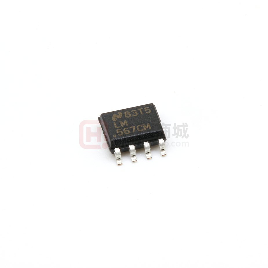
LM567CM/NOPB
ACTIVE
SOIC
D
8
95
Green (RoHS
& no Sb/Br)
CU SN
Level-1-260C-UNLIM
0 to 70
LM
567CM
LM567CMX/NOPB
ACTIVE
SOIC
D
8
2500
Green (RoHS
& no Sb/Br)
CU SN
Level-1-260C-UNLIM
0 to 70
LM
567CM
LM567CN/NOPB
ACTIVE
PDIP
P
8
40
Green (RoHS
& no Sb/Br)
CU SN
Level-1-NA-UNLIM
0 to 70
LM
567CN
(1)
The marketing status values are defined as follows:
ACTIVE: Product device recommended for new designs.
LIFEBUY: TI has announced that the device will be discontinued, and a lifetime-buy period is in effect.
NRND: Not recommended for new designs. Device is in production to support existing customers, but TI does not recommend using this part in a new design.
PREVIEW: Device has been announced but is not in production. Samples may or may not be available.
OBSOLETE: TI has discontinued the production of the device.
(2)
RoHS: TI defines "RoHS" to mean semiconductor products that are compliant with the current EU RoHS requirements for all 10 RoHS substances, including the requirement that RoHS substance
do not exceed 0.1% by weight in homogeneous materials. Where designed to be soldered at high temperatures, "RoHS" products are suitable for use in specified lead-free processes. TI may
reference these types of products as "Pb-Free".
RoHS Exempt: TI defines "RoHS Exempt" to mean products that contain lead but are compliant with EU RoHS pursuant to a specific EU RoHS exemption.
Green: TI defines "Green" to mean the content of Chlorine (Cl) and Bromine (Br) based flame retardants meet JS709B low halogen requirements of