Order
Now
Product
Folder
Support &
Community
Tools &
Software
Technical
Documents
Reference
Design
LM73605, LM73606
SNVSAH5A – SEPTEMBER 2017 – REVISED MAY 2020
LM73605/LM73606 3.5-V to 36-V, 5-A or 6-A Synchronous
Step-Down Voltage Converter
1 Features
2 Applications
•
•
•
•
1
•
•
•
•
•
•
•
•
•
•
•
•
•
•
•
•
New product available: LM61460 60-V, 6-A
synchronous converter
Synchronous rectification
Wettable flanks QFN package (WQFN)
Low quiescent current
– 0.8 µA in shutdown (typical)
– 15 µA in active mode with no load (typical)
Wide voltage conversion range:
– tON-MIN = 60 ns (typical)
– tOFF-MIN = 70 ns (typical)
Low MOSFET ON-resistance:
– RDS_ON_HS = 53 mΩ (typical)
– RDS_ON_LS = 31 mΩ (typical)
External bias input to improve efficiency
Pin-selectable auto mode or forced PWM
operation
Adjustable frequency range: 350 kHz to 2.2 MHz
Synchronizable to external clock
Internal compensation
Power-good flag
Precision enable to program system UVLO
Flexible soft-start features:
– Start-up into pre-biased load
– Fixed or adjustable soft-start time
– Output voltage tracking
Cycle-by-cycle current limiting
Short-circuit protection with hiccup mode
Create a custom design with the WEBENCH®
power designer using LM73605 or LM73606
Simplified Schematic
L
VIN
PVIN
CIN
VOUT
Industrial distributed power applications
Test and measurement
General-purpose wide VIN applications
3 Description
The LM73605 and LM73606 family of devices are
easy-to-use
synchronous
step-down
DC/DC
converters capable of driving up to 5 A or 6 A of load
current from a supply voltage ranging from 3.5 V to
36 V. The LM73605 and LM73606 provide
exceptional efficiency and output accuracy in a very
small solution size. Peak current-mode control is
employed. Additional features such as adjustable
switching frequency, synchronization to an external
clock, power-good flag, precision enable, adjustable
soft start, and tracking provide both flexible and easyto-use solutions for a wide range of applications.
Automatic frequency foldback at light load improves
efficiency over the entire load range. Protection
features include thermal shutdown, cycle-by-cycle
current limiting, and short-circuit protection. The
devices are pin-to-pin compatible for easy current
scaling. The new product, LM61460-Q1, offers higher
efficiency, lower stand-by quiescent current, and
improved EMI performance. See the device
comparison table to compare specifications. Start a
Webench design with LM61460-Q1. Use the
LMZM33606 module for faster time to market.
Device Information(1)
PART NUMBER
LM73605
LM73606
PACKAGE
BODY SIZE (NOM)
WQFN (30)
Wettable Flanks
6.00 mm × 4.00 mm
(1) For all available packages, see the orderable addendum at
the end of the data sheet.
Efficiency versus Load Current
VOUT = 5 V, fSW = 500 kHz, Auto Mode
SW
100
CBOOT
COUT
95
EN
90
CBOOT
PGND
SS/TRK
RT
SYNC/
MODE
RFBT
FB
Efficiency (%)
85
PGOOD
BIAS
80
75
70
65
RFBB
VCC
CVCC
60
VIN = 12 V
VIN = 24 V
AGND
55
50
0.001
0.01 0.02 0.05 0.1 0.2
Load Current (A)
0.5
1
2 3 4 56
Eff_
1
An IMPORTANT NOTICE at the end of this data sheet addresses availability, warranty, changes, use in safety-critical applications,
intellectual property matters and other important disclaimers. PRODUCTION DATA.
�LM73605, LM73606
SNVSAH5A – SEPTEMBER 2017 – REVISED MAY 2020
www.ti.com
Table of Contents
1
2
3
4
5
6
7
Features ..................................................................
Applications ...........................................................
Description .............................................................
Revision History.....................................................
Pin Configuration and Functions .........................
Specifications.........................................................
1
1
1
2
3
5
6.1
6.2
6.3
6.4
6.5
6.6
6.7
6.8
6.9
5
5
5
6
6
8
8
8
9
Absolute Maximum Ratings ......................................
ESD Ratings..............................................................
Recommended Operating Conditions.......................
Thermal Information ..................................................
Electrical Characteristics...........................................
Timing Characteristics...............................................
Switching Characteristics ..........................................
System Characteristics .............................................
Typical Characteristics ..............................................
Detailed Description ............................................ 11
7.1 Overview ................................................................. 11
7.2 Functional Block Diagram ....................................... 11
7.3 Feature Description................................................. 12
7.4 Device Functional Modes........................................ 24
8
Application and Implementation ........................ 26
8.1 Application Information............................................ 26
8.2 Typical Application ................................................. 26
9 Power Supply Recommendations...................... 40
10 Layout................................................................... 40
10.1 Layout Guidelines ................................................. 40
10.2 Layout Example .................................................... 43
11 Device and Documentation Support ................. 44
11.1
11.2
11.3
11.4
11.5
11.6
11.7
11.8
Device Support......................................................
Documentation Support ........................................
Related Links ........................................................
Receiving Notification of Documentation Updates
Support Resources ...............................................
Trademarks ...........................................................
Electrostatic Discharge Caution ............................
Glossary ................................................................
44
44
44
44
45
45
45
45
12 Mechanical, Packaging, and Orderable
Information ........................................................... 45
4 Revision History
Changes from Original (September 2017) to Revision A
Page
•
Added bullet point for new product......................................................................................................................................... 1
•
Added wording for new product.............................................................................................................................................. 1
2
Submit Documentation Feedback
Copyright © 2017–2020, Texas Instruments Incorporated
Product Folder Links: LM73605 LM73606
�LM73605, LM73606
www.ti.com
SNVSAH5A – SEPTEMBER 2017 – REVISED MAY 2020
5 Pin Configuration and Functions
RNP Package
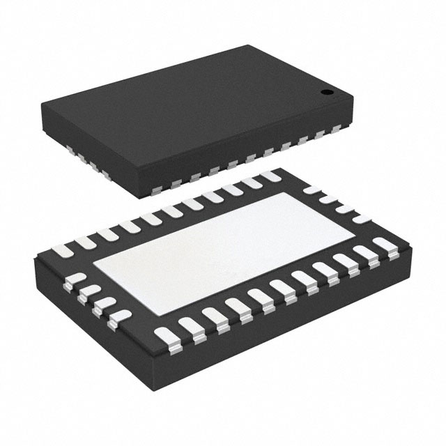
30-Pin Wettable Flanks QFN (WQFN) 6 mm × 4 mm × 0.8 mm
Top View
NC
NC
NC
NC
30
29
28
27
SW
1
26
PGND
SW
2
25
PGND
SW
3
24
PGND
SW
4
23
PGND
SW
5
22
PVIN
CBOOT
6
21
PVIN
VCC
7
20
PVIN
BIAS
8
19
AGND
RT
9
18
EN
SS/TRK
10
17
SYNC/
MODE
FB
11
16
PGOOD
DAP
12
13
14
15
NC
NC
NC
NC
Pin Functions
PIN
I/O (1)
DESCRIPTION
SW
P
Switching output of the regulator. Internally connected to source of the HS FET and drain of the LS
FET. Connect to power inductor and bootstrap capacitor.
6
CBOOT
P
Bootstrap capacitor connection for HS FET driver. Connect a high-quality 470-nF capacitor from
this pin to the SW pin.
7
VCC
P
Output of internal bias supply. Used as supply to internal control circuits and drivers. Connect a
high-quality 2.2-µF capacitor from this pin to GND. TI does not recommend loading this pin by
external circuitry.
8
BIAS
P
Optional BIAS LDO supply input. TI recommends tying to VOUT when 3.3 V ≤ VOUT ≤ 18 V, or tie to
an external 3.3-V or 5-V rail if available, to improve efficiency. BIAS pin voltage must not be
greater than VIN. Tie to ground when not in use.
9
RT
A
Switching frequency setting pin. Place a resistor from this pin to ground to set the switching
frequency. If floating, the default switching frequency is 500 kHz. Do not short to ground.
NO.
NAME
1, 2, 3, 4, 5
(1)
10
SS/TRK
A
Soft-start control pin. Leave this pin floating for a fixed internal soft-start ramp. An external
capacitor can be connected from this pin to ground to extend the soft start time. A 2-µA current
sourced from this pin charges the capacitor to provide the ramp. Connect to external ramp for
tracking. Do not short to ground.
11
FB
I
Feedback input for output voltage regulation. Connect a resistor divider to set the output voltage.
Never short this pin to ground during operation.
12–15,
27–30
NC
—
No internal connection. Connect to ground net and copper to improve heat sinking and board-level
reliability.
16
PGOOD
O
Open drain power-good flag output. Connect to suitable voltage supply through a current limiting
resistor. High = VOUT regulation OK, Low = VOUT regulation fault. PGOOD = LOW when EN = low
and VIN > 2 V.
A = Analog, O = Output, I = Input, G = Ground, P = Power
Copyright © 2017–2020, Texas Instruments Incorporated
Product Folder Links: LM73605 LM73606
Submit Documentation Feedback
3
�LM73605, LM73606
SNVSAH5A – SEPTEMBER 2017 – REVISED MAY 2020
www.ti.com
Pin Functions (continued)
PIN
4
I/O (1)
DESCRIPTION
SYNC/MODE
I
Synchronization input and mode setting pin. Do not float. Tie to ground if not used.
Tie to ground: auto mode, higher efficiency at light loads;
Tie to logic high: forced PWM, constant switching frequency over load;
Tie to external clock source: forced PWM, synchronize to the rising edge of the external clock.
18
EN
I
Enable input to regulator. Do not float. High = ON, Low = OFF. Can be tied to PVIN. Precision
enable input allows adjustable input voltage UVLO using external resistor divider.
19
AGND
G
Analog ground. Ground reference for internal circuitry. All electrical parameters are measured with
respect to this pin. Connect to system ground on PCB.
20–22
PVIN
P
Supply input to internal bias LDO and HS FET. Connect to input supply and input bypass
capacitors CIN. CIN must be placed right next to this pin and PGND pins on PCB, and connected
with short and wide traces.
23–26
PGND
G
Power ground, connected to the source of LS FET internally. Connect to system ground, DAP/EP,
AGND, ground side of CIN and COUT on PCB. Path to CIN must be as short as possible
EP
DAP
G
Low impedance connection to AGND. Connect to system ground on PCB. Major heat dissipation
path for the device. Must be used for heat sinking by soldering to ground copper on PCB. Thermal
vias are preferred to improve heat dissipation to other layers.
NO.
NAME
17
Submit Documentation Feedback
Copyright © 2017–2020, Texas Instruments Incorporated
Product Folder Links: LM73605 LM73606
�LM73605, LM73606
www.ti.com
SNVSAH5A – SEPTEMBER 2017 – REVISED MAY 2020
6 Specifications
6.1 Absolute Maximum Ratings
Over operating free-air temperature range of –40°C to +125°C (unless otherwise noted) (1)
MIN
MAX
PVIN to PGND
PARAMETER
–0.3
42
EN to AGND
–0.3
VIN + 0.3
FB, RT, SS/TRK to AGND
–0.3
5
PGOOD to AGND
–0.1
20
SYNC to AGND
–0.3
5.5
BIAS to AGND
–0.3
Lower of (VIN + 0.3) or 20
AGND to PGND
–0.3
0.3
SW to PGND
–0.3
VIN + 0.3
SW to PGND less than 10-ns transients
–3.5
42
CBOOT to SW
–0.3
5
VCC to AGND
–0.3
5
Junction temperature, TJ
–40
150
°C
Storage temperature, Tstg
–65
150
°C
Input voltages
Output voltages
(1)
UNIT
V
V
Stresses beyond those listed under Absolute Maximum Ratings may cause permanent damage to the device. These are stress ratings
only, which do not imply functional operation of the device at these or any other conditions beyond those indicated under Recommended
Operating Conditions. Exposure to absolute-maximum-rated conditions for extended periods may affect device reliability.
6.2 ESD Ratings
VALUE
V(ESD)
(1)
(2)
Electrostatic discharge
Human-body model (HBM), per ANSI/ESDA/JEDEC JS-001 (1)
±2000
Charged-device model (CDM), per JEDEC specification JESD22-C101 (2)
±750
UNIT
V
JEDEC document JEP155 states that 500-V HBM allows safe manufacturing with a standard ESD control process.
JEDEC document JEP157 states that 250-V CDM allows safe manufacturing with a standard ESD control process.
6.3 Recommended Operating Conditions
Over operating free-air temperature range of –40°C to +125°C (unless otherwise noted) (1)
PVIN to PGND
Input voltages
Output voltage
Output current
(1)
MIN
MAX
3.5
36
UNIT
EN
0
VIN
FB
0
4.5
PGOOD
0
18
BIAS input not used
0
0.3
BIAS input used
0
Lower of (VIN + 0.3) or 18
AGND to PGND
–0.1
0.1
VOUT
1
95% of VIN
V
IOUT, LM73605
0
5
A
IOUT, LM73606
0
6
A
V
Recommended operating rating indicate conditions for which the device is intended to be functional, but do not ensure specific
performance limits. For ensured specifications, see Electrical Characteristics
Copyright © 2017–2020, Texas Instruments Incorporated
Product Folder Links: LM73605 LM73606
Submit Documentation Feedback
5
�LM73605, LM73606
SNVSAH5A – SEPTEMBER 2017 – REVISED MAY 2020
www.ti.com
6.4 Thermal Information
LM73605/LM73606
THERMAL METRIC (1)
RNP (WQFN)
UNIT
30 PINS
RθJA
Junction-to-ambient thermal resistance
34.3
°C/W
RθJC(top)
Junction-to-case (top) thermal resistance
14.6
°C/W
RθJB
Junction-to-board thermal resistance
7.3
°C/W
ψJT
Junction-to-top characterization parameter
0.1
°C/W
ψJB
Junction-to-board characterization parameter
7.1
°C/W
RθJC(bot)
Junction-to-case (bottom) thermal resistance
1
°C/W
(1)
For more information about traditional and new thermal metrics, see the Semiconductor and IC Package Thermal Metrics application
report.
6.5 Electrical Characteristics
Limits apply over the recommended operating junction temperature (TJ) range of –40°C to +125°C, unless otherwise stated.
Minimum and maximum limits are specified through test, design or statistical correlation. Typical values represent the most
likely parametric norm at TJ = 25°C, and are provided for reference purposes only. Unless otherwise stated, VIN = 12 V.
PARAMETER
TEST CONDITIONS
MIN
TYP
MAX
UNIT
SUPPLY VOLTAGE (PVIN PINS)
VIN
Operating input voltage
range
ISD
Shutdown quiescent current;
measured at VIN pin (1)
VEN = 0 V
TJ = 25℃
IQ_NONSW
Operating quiescent current
from VIN (non-switching)
VEN = 2 V, VFB = 1.5 V, VBIAS = 3.3 V
external
3.5
36
V
0.8
10
µA
0.6
12
µA
1.15
V
ENABLE (EN PIN)
VEN_VCC_H
Enable input high level for
VCC output
VEN rising
VEN_VCC_L
Enable input low level for
VCC output
VEN falling
0.3
VEN_VOUT_H
Enable input high level for
VOUT
VEN rising
1.14
VEN_VOUT_HYS
Enable input hysteresis for
VOUT
VEN falling hysteresis
ILKG_EN
Enable input leakage current
VEN = 2 V
V
1.196
1.25
–100
1.4
V
mV
200
nA
INTERNAL LDO (VCC PIN, BIAS PIN)
VCC
Internal VCC voltage
VCC_UVLO
Internal VCC undervoltage
lockout
VBIAS_ON
Input changeover
IBIAS_NONSW
Operating quiescent current
from external VBIAS (nonswitching)
PWM operation
3.27
V
PFM operation
3.1
V
VCC rising
2.96
3.14
VCC falling hysteresis
–605
VBIAS rising
3.09
VBIAS falling hysteresis
–63
VEN = 2 V, VFB = 1.5 V, VBIAS = 3.3 V
external
3.27
V
mV
3.25
V
mV
21
50
µA
1.006
1.017
V
0.2
60
nA
VOLTAGE REFERENCE (FB PIN)
VFB
Feedback voltage
PWM mode
ILKG_FB
Input leakage current at FB
pin
VFB = 1 V
(1)
6
0.987
Shutdown current includes leakage current of the switching transistors.
Submit Documentation Feedback
Copyright © 2017–2020, Texas Instruments Incorporated
Product Folder Links: LM73605 LM73606
�LM73605, LM73606
www.ti.com
SNVSAH5A – SEPTEMBER 2017 – REVISED MAY 2020
Electrical Characteristics (continued)
Limits apply over the recommended operating junction temperature (TJ) range of –40°C to +125°C, unless otherwise stated.
Minimum and maximum limits are specified through test, design or statistical correlation. Typical values represent the most
likely parametric norm at TJ = 25°C, and are provided for reference purposes only. Unless otherwise stated, VIN = 12 V.
PARAMETER
TEST CONDITIONS
MIN
TYP
MAX
1.6
2.2
2.7
LM73605
6
7.3
8.35
LM73606
7.4
8.7
9.85
LM73605
4.79
5.5
6.1
LM73606
5.8
6.6
7.25
UNIT
HIGH SIDE DRIVER (CBOOT PIN)
VCBOOT_UVLO
CBOOT - SW undervoltage
lockout
V
CURRENT LIMITS AND HICCUP
IHS_LIMIT
Short-circuit, high-side
current limit (2)
ILS_LIMIT
Low-side current limit (2)
INEG_LIMIT
Negative current limit
VHICCUP
Hiccup threshold on FB pin
IL_ZC
Zero cross-current limit
LM73605
–5
LM73606
–6
0.36
0.4
A
A
A
0.44
0.06
V
A
SOFT START (SS/TRK PIN)
ISSC
Soft-start charge current
RSSD
Soft-start discharge
resistance
1.8
UVLO, TSD, OCP, or EN = 0
2
2.2
1
µA
kΩ
POWER GOOD (PGOOD PIN) and OVERVOLTAGE PROTECTION
VPGOOD_OV
Power-good overvoltage
threshold
% of FB voltage
106%
110%
113%
VPGOOD_UV
Power-good undervoltage
threshold
% of FB voltage
86%
90%
93%
VPGOOD_HYS
Power-good hysteresis
% of FB voltage
VPGOOD_VALID
Minimum input voltage for
proper PGOOD function
50-µA pullup to PGOOD pin, VEN = 0 V,
TJ = 25°C
1.3
2
RPGOOD
Power-good ON-resistance
VEN = 2.5V
40
100
VEN = 0 V
30
90
1.2%
V
Ω
MOSFETS
RDS_ON_HS (3)
High-side MOSFET ONresistance
IOUT = 1 A, VBIAS = VOUT = 3.3 V
53
90
mΩ
RDS_ON_LS (3)
Low-side MOSFET ONresistance
IOUT = 1 A, VBIAS = VOUT = 3.3 V
31
55
mΩ
THERMAL SHUTDOWN
TSD (4)
(2)
(3)
(4)
Thermal shutdown threshold
Shutdown threshold
Recovery threshold
160
°C
135
°C
This current limit was measured as the internal comparator trip point. Due to inherent delays in the current limit comparator and drivers,
the peak current limit measured in closed loop with faster slew rate will be larger, and valley current limit will be lower.
Measured at pins
Ensured by design
Copyright © 2017–2020, Texas Instruments Incorporated
Product Folder Links: LM73605 LM73606
Submit Documentation Feedback
7
�LM73605, LM73606
SNVSAH5A – SEPTEMBER 2017 – REVISED MAY 2020
www.ti.com
6.6 Timing Characteristics
MIN
NOM
MAX
UNIT
CURRENT LIMITS AND HICCUP
NOC (1)
Number of switching cycles before
hiccup is tripped
128
Cycles
tOC
Overcurrent hiccup retry delay time
46
ms
3.5
6.3
ms
SOFT START (SS/TRK PIN)
tSS
CSS = OPEN, from EN rising edge to
PGOOD rising edge
Internal soft-start time
POWER GOOD (PGOOD PIN) and OVERVOLTAGE PROTECTION
tPGOOD_RISE
PGOOD rising edge deglitch delay
80
140
200
µs
tPGOOD_FALL
PGOOD falling edge deglitch delay
80
140
200
µs
MAX
UNIT
(1)
Ensured by design
6.7 Switching Characteristics
PARAMETER
TEST CONDITIONS
MIN
TYP
PWM LIMITS (SW PINS)
tON-MIN
Minimum switch on-time
60
82
tOFF-MIN
Minimum switch off-time
70
120
ns
tON-MAX
Maximum switch on-time
3
6
9
µs
HS timeout in dropout
ns
OSCILLATOR (RT and SYNC PINS)
fOSC
fADJ
Internal oscillator frequency
RT = Open
440
500
560
kHz
Minimum adjustable frequency by RT or
SYNC
RT =115 kΩ, 0.1%
315
350
385
kHz
Maximum adjustable frequency by RT or
SYNC
RT = 17.4 kΩ, 0.1%
1980
2200
2420
kHz
VSYNC_HIGH
Sync input high level threshold
VSYNC_LOW
Sync input low level threshold
2
VMODE_HIGH
Mode input high level threshold for
FPWM
VMODE_LOW
tSYNC_MIN
0.4
V
V
0.42
V
Mode input low level threshold for AUTO
mode
0.4
V
Sync input minimum ON and OFF-time
80
ns
6.8 System Characteristics
The following specifications apply to the circuit found in typical schematic with appropriate modifications from typical bill of
materials. These parameters are not tested in production and represent typical performance only. Unless otherwise stated the
following conditions apply: TA = 25°C, VIN = 12 V, VOUT = 3.3 V, fSW = 500 kHz.
PARAMETER
TEST CONDITIONS
MIN
TYP
MAX
UNIT
VFB_PFM
Output voltage offset at no load in
auto mode
VIN = 3.8 V to 36 V, VSYNC = 0 V, auto mode IOUT = 0
A
2%
VDROP
Minimum input to output voltage
differential to maintain specified
accuracy
VOUT = 5 V, IOUT = 3 A, fSW = 2.2 MHz
0.4
V
IQ_SW
Operating quiescent current
(switching)
VEN = 3.3 V, IOUT = 0 A, RT = open, VBIAS = VOUT =
3.3 V , RFBT = 1 Meg
15
µA
IPEAK_MIN
Minimum inductor peak current
LM73605:
VSYNC = 0, IOUT = 10 mA
1
A
LM73606:
VSYNC = 0 V, IOUT = 10 mA
1.3
IBIAS_SW
Operating quiescent current from
external VBIAS (switching)
fSW = 500 kHz, IOUT = 1 A
7
fSW = 2.2 MHz, IOUT = 1 A
25
DMAX
Maximum switch duty cycle
While in frequency foldback
tDEAD
Dead time between high-side and
low-side MOSFETs
8
Submit Documentation Feedback
mA
97.5%
4
ns
Copyright © 2017–2020, Texas Instruments Incorporated
Product Folder Links: LM73605 LM73606
�LM73605, LM73606
www.ti.com
SNVSAH5A – SEPTEMBER 2017 – REVISED MAY 2020
6.9 Typical Characteristics
Unless otherwise specified, VIN = 12 V. Curves represent most likely parametric norm at specified condition.
75
70
HS Switch
LS Switch
Shutdown Current (nA)
65
RDS-ON (m:)
60
55
50
45
40
35
30
25
20
-40
-20
0
20
40
60
80
Temperature (°C)
100
120
140
1600
1500
1400
1300
1200
1100
1000
900
800
700
600
500
400
300
200
-40
-20
0
CHAR
Figure 1. High-Side and Low-Side Switches RDS-ON
20
40
60
Temperature (°C)
80
100
120
CHAR
Plot
Figure 2. Shutdown Quiescent Current
1.01
7.5
Temp = -40°C
Temp = 25°C
Temp = 125°C
1.009
1.008
7
1.007
Current Limits (A)
Feedback Voltage (V)
VIN = 3.5 V
VIN = 12 V
VIN = 36 V
1.006
1.005
1.004
1.003
1.002
6.5
HS
LS
6
5.5
1.001
1
3
6
9
12
15
18 21
VIN (V)
24
27
30
33
5
-40
36
-20
0
CHAR
Figure 3. Feedback Voltage
20
40
60
Temperature (°C)
80
100
120
CHAR
Figure 4. LM73605 High-Side and Low-Side Current Limits
2500
9
2250
2000
Frequency (kHz)
Current Limits (A)
8.4
7.8
HS
LS
7.2
FREQ = 350 kHz
FREQ = 1 MHz
FREQ = 2.2 MHz
1750
1500
1250
1000
750
500
6.6
250
6
-40
-20
0
20
40
60
Temperature (°C)
80
100
0
-40
120
-20
CHAR
Figure 5. LM73605 High-Side and Low-Side Current Limit
0
20
40
60
Temperature (°C)
80
100
120
CHAR
Figure 6. Switching Frequency Set by RT Resistor
Copyright © 2017–2020, Texas Instruments Incorporated
Product Folder Links: LM73605 LM73606
Submit Documentation Feedback
9
�LM73605, LM73606
SNVSAH5A – SEPTEMBER 2017 – REVISED MAY 2020
www.ti.com
Typical Characteristics (continued)
550
1.28
540
1.2
530
1.12
Enable Thresholds (V)
Frequency with RT Pin Floating (kHz)
Unless otherwise specified, VIN = 12 V. Curves represent most likely parametric norm at specified condition.
520
510
500
490
480
VIN = 3.5 V
VIN = 12 V
VIN = 36 V
470
460
450
-40
-20
0
20
40
60
Temperature (°C)
80
100
1.04
VEN_VOUT Rising
VEN_VOUT Falling
VEN_VCC Rising
VEN_VCC Falling
0.96
0.88
0.8
0.72
0.64
0.56
-40
120
-20
0
20
CHAR
Figure 7. Switching Frequency with RT Pin Open Circuit
40
60
80
Temperature (°C)
100
120
140
CHAR
Figure 8. Enable Thresholds
115
PGOOD Thresholds (%)
110
105
OV Tripping
OV Recovery
UV Recovery
UV Tripping
100
95
90
85
-40
-20
0
20
40
60
Temperature (°C)
80
100
120
CHAR
Figure 9. PGOOD Thresholds
10
Submit Documentation Feedback
Copyright © 2017–2020, Texas Instruments Incorporated
Product Folder Links: LM73605 LM73606
�LM73605, LM73606
www.ti.com
SNVSAH5A – SEPTEMBER 2017 – REVISED MAY 2020
7 Detailed Description
7.1 Overview
The LM73605 and LM73606 are easy-to-use synchronous step-down DC/DC converters that operate from a 3.5V to 36-V supply voltage. It is capable of delivering up to 5-A (LM73605) or 6-A (LM73606) DC load current with
exceptional efficiency and thermal performance in a very small solution size.
The LM73605 and LM73606 employs fixed-frequency peak current-mode control with configurable auto or
FPWM operation mode. Auto mode provides very high efficiency at light loads, and FPWM mode maintains
constant switching frequency over entire load range.
The device is internally compensated, which reduces design time and the number of external components. The
switching frequency is programmable from 350 kHz to 2.2 MHz by an external resistor. The LM73605 and
LM73606 can also synchronize to an external clock within the same frequency range. The wide switching
frequency range allows the device to be optimized for a wide range of system requirements. It can be optimized
for small solution size with higher frequency; or for high efficiency with lower switching frequency. The LM73605
and LM73606 have very low quiescent current, which is critical for battery-operated systems. It allows for a wide
range of voltage conversion ratios due to very small minimum on-time (tON-MIN) and minimum off-time (tOFF-MIN).
Automated frequency foldback is employed at very high or low duty cycles to further extend the operating range.
The LM73605 and LM73606 also feature a power-good (PGOOD) flag, precision enable, internal or adjustable
soft start, pre-biased start-up, and output voltage tracking. Protection features include thermal shutdown,
undervoltage lockout (UVLO), cycle-by-cycle current limiting, and short-circuit hiccup protection. It provides
flexible and easy-to-use solutions for a wide range of applications.
The family requires very few external components and has a pin out designed for simple, optimum PCB layout
for enhanced EMI and thermal performance. The LM73605 and LM73606 devices are available in a 30-pin
WQFN leadless package.
7.2 Functional Block Diagram
VCC
ENABLE
ISSC
BIAS
LDO
Internal
SS
CBOOT
VCC
SS/TRK
HS I Sense
ICMD +
EA
REF
VBOOT VSW
+
±
RC
FB
FB
OV/UV
Detector
± +
UVLO
UVLO
CC
VSW
PFM
Detector
CONTROL LOGIC
SW
PGood
Hiccup
Detector
Slope Comp
Oscillator
TSD
± +
PGOOD
PVIN
VBOOT
Precision
Enable
CLK
ILIMIT
AGND
FPWM
RT
SYNC/
MODE
LS I Sense
PGND
Copyright © 2017–2020, Texas Instruments Incorporated
Product Folder Links: LM73605 LM73606
Submit Documentation Feedback
11
�LM73605, LM73606
SNVSAH5A – SEPTEMBER 2017 – REVISED MAY 2020
www.ti.com
7.3 Feature Description
7.3.1 Synchronous Step-Down Regulator
The LM73605 and LM73606 are synchronous buck converters with both power MOSFETs integrated in the
device. Figure 10 shows a simplified schematic for synchronous and non-synchronous buck converters. The
synchronous buck integrates both high-side (HS) and low-side (LS) power MOSFETs. The non-synchronous
buck integrates HS MOSFET and works with a discrete power diode as LS rectifier.
VIN
VIN
Synchronous
Buck
L
SW
CIN
VOUT
COUT
VIN
VIN
Non Synchronous
Buck
SW
L
CIN
VOUT
COUT
PGND
PGND
Figure 10. Simplified Synchronous versus Non-synchronous Buck Converters
A
•
•
•
•
•
•
synchronous converter with integrated HS and LS MOSFETs offers benefits such as the following:
Less design effort
Lower external component count
Reduced total solution size
Higher efficiency at heavier load
Easier PCB design
More control flexibility
The main advantage of a synchronous converter is that the voltage drop across the LS MOSFET is lower than
the voltage drop across the power diode of a non-synchronous converter. Lower voltage drop translates into less
power dissipation and higher efficiency. The LM73605 and LM73606 integrate HS and LS MOSFETs with very
low on-time resistance to improve efficiency. It is especially beneficial when the output voltage is low. Because
the LS MOSFET is integrated into these devices, at light loads a synchronous converter has the flexibility to
operate in either discontinuous or continuous conduction mode.
An integrated LS MOSFET also allows the controller to obtain inductor current information when the LS switch is
on. It allows the control loop to make more complex decisions based on HS and LS currents. It allows the
LM73605 and LM73606 to have peak and valley cycle-by-cycle current limiting for more robust protection.
7.3.2 Auto Mode and FPWM Mode
The LM73605 and LM73606 have pin-configurable auto mode or FPWM options.
In auto mode, the device operates in diode emulation mode (DEM) at light loads. In DEM, inductor current stops
flowing when it reaches 0 A. This is also referred to as discontinuous conduction mode (DCM). This is the same
behavior as the non-synchronous regulator, with higher efficiency. At heavier load, when the inductor current
valley is above 0 A, the device operates in continuous conduction mode (CCM), where the switching frequency is
fixed and set by RT pin.
In auto mode, the peak inductor current has a minimum limit, IPEAK_MIN, in the LM73605 and LM73606. When
peak current reaches IPEAK_MIN, the switching frequency reduces to regulate the required load current. Switching
frequency lowers when load reduces. This is when the device operates in pulse frequency modulation (PFM).
PFM further improves efficiency by reducing switching losses. Light load efficiency is especially important for
battery-operated systems.
In forced PWM (FPWM) mode, the device operates in CCM regardless of load with the frequency set by RT pin
or synchronization input. Inductor current can go negative at light loads. At light loads, the efficiency is lower than
auto mode, due to higher conduction losses and switching losses. In FPWM, the device has fixed switching
frequency over the entire load range, which is beneficial to noise sensitive applications.
12
Submit Documentation Feedback
Copyright © 2017–2020, Texas Instruments Incorporated
Product Folder Links: LM73605 LM73606
�LM73605, LM73606
www.ti.com
SNVSAH5A – SEPTEMBER 2017 – REVISED MAY 2020
Feature Description (continued)
Figure 11 shows the inductor current waveforms in each mode with heavy load, light load, and very light load.
The difference between the two modes is at lighter loads where inductor current valley reaches zero.
Auto Mode
IL
FPWM Mode
IL
CCM
CCM
Heavy
Loads
t
Light
Loads
t
IL
IL
CCM
DCM
t
IL
t
IL
PFM
CCM
Very Light
Loads
t
t
Figure 11. Inductor Current Waveforms at Auto Mode and FPWM Mode with Different Loads
In CCM, the inductor current peak-to-peak ripple can be estimated by Equation 1:
ILripple =
(VIN VOUT )
V
u OUT
fSW u L
VIN
(1)
The average or DC value of the inductor current equals the load current, or output current IOUT, in steady state.
Peak inductor current can be calculated by Equation 2:
IPEAK = IOUT + ILripple / 2
(2)
Valley inductor current can be calculated by Equation 3:
IVALLEY = IOUT – ILripple / 2
(3)
In auto mode, the CCM-to-DCM boundary condition is when IVALLEY = 0 A. When ILripple ≥ IPEAK_MIN, the load
current at the DCM boundary condition can be found by Equation 4. When the peak-to-peak ripple current is
smaller than ILripple ≥ IPEAK-MIN, the PFM boundary is reached first.
IOUT_DCM = ILripple / 2
when
•
ILripple ≥ IPEAK_MIN
(4)
In auto mode, the PFM operation boundary condition is when IPEAK = IPEAK_MIN. Frequency foldback occurs when
peak current drops to IPEAK_MIN, regardless of whether it is in CCM or DCM operation. When current ripple is
small, ILripple < IPEAK_MIN, the peak current reaches IPEAK_MIN when it is still in CCM. The output current at CCM
PFM boundary can be found by Equation 5:
IOUT_CCM_PFM = IPEAK_MIN – ILripple / 2
when
•
ILripple < IPEAK_MIN
(5)
The current ripple increases with reduced frequency if load reduces. When valley current reaches zero, the
frequency continues to fold back with constant peak current and discontinuous current.
In FPWM mode, there is no IPEAK-MIN limit. The peak current is defined by Equation 2 at light loads and heavy
loads.
Mode setting only affects operation at light loads. There is no difference if load current is above the DCM and
PFM boundary conditions discussed above.
See the Frequency Synchronization and Mode Setting section for mode setting options in the LM73605 and
LM73606.
Copyright © 2017–2020, Texas Instruments Incorporated
Product Folder Links: LM73605 LM73606
Submit Documentation Feedback
13
�LM73605, LM73606
SNVSAH5A – SEPTEMBER 2017 – REVISED MAY 2020
www.ti.com
Feature Description (continued)
7.3.3 Fixed-Frequency Peak Current-Mode Control
The LM73605 and LM73606 synchronous switched mode voltage regulator employs fixed frequency peak current
mode control with advanced features. The fixed switching frequency is controlled by an internal clock. To get
accurate DC load regulation, a voltage feedback loop is implemented to generate peak current command. The
HS switch is turned on at the rising edge of the clock. As shown in Figure 12, during the HS switch on-time, tON,
the SW pin voltage, VSW, swings up to approximately VIN, and the inductor current, IL, increases with a linear
slope. The HS switch is turned off when the inductor current reaches the peak current command. During the HS
switch off-time, tOFF, the LS switch is turned on. Inductor current discharges through the LS switch, which forces
the VSW to swing below ground by the voltage drop across the LS switch. The LS switch is turned off at the next
clock cycle, before the HS switch is turned on. The regulation loop adjusts the peak current command to
maintain a constant output voltage.
VSW
SW Voltage
D = tON / TSW
VIN
tON
tOFF
0
-VD
t
TSW
Inductor Current
IL
IL-PEAK
IOUT
ILripple
IL-VALLEY
t
0
Figure 12. SW Voltage and Inductor Current Waveforms in CCM
Duty cycle D is defined by the on-time of the HS switch over the switching period:
D = tON / TSW
where
•
TSW = 1 / fSW is the switching period
(6)
In an ideal buck converter where losses are ignored, D is proportional to the output voltage and inverse
proportional to the input voltage: D = VOUT ⁄ VIN.
When the LM73605 and LM73606 are set to operate in auto mode, the LS switch is turned off when its current
reaches zero ampere before the next clock cycle comes. Both HS switch and LS switch are off before the HS
switch is turned on at the next clock cycle.
7.3.4 Adjustable Output Voltage
The voltage regulation loop in the LM73605 and LM73606 regulate the FB pin voltage to be the same as the
internal reference voltage. The output voltage of the LM73605 and LM73606 is set by a resistor divider to
program the ratio from VOUT to VFB. The resistor divider is connected from the output to ground with the mid-point
connecting to the FB pin.
VOUT
RFBT
FB
RFBB
Figure 13. Output Voltage Setting by Resistor Divider
14
Submit Documentation Feedback
Copyright © 2017–2020, Texas Instruments Incorporated
Product Folder Links: LM73605 LM73606
�LM73605, LM73606
www.ti.com
SNVSAH5A – SEPTEMBER 2017 – REVISED MAY 2020
Feature Description (continued)
The internal voltage reference and feedback loop produce precise voltage regulation over temperature. TI
recommends using divider resistors with 1% tolerance or better, and with temperature coefficient of 100 ppm or
lower. Typically, RFBT = 10 kΩ to 100 kΩ is recommended. Larger RFBT and RFBB values reduce the quiescent
current going through the divider, which help maintain high efficiency at very light load. Larger divider values also
make the feedback path more susceptible to noise. If efficiency at very light load is critical in a certain
application, RFBT up to 1 MΩ can be used.
RFBB can be calculated by Equation 7:
VFB
RFBB
RFBT
VOUT VFB
(7)
The minimum programmable VOUT equals VFB, with RFBB open. The maximum VOUT is limited by the maximum
duty cycle at a given frequency:
DMAX = 1 – (tOFF-MIN / TSW)
where
•
•
tOFF-MIN is the minimum off time of the HS switch
TSW = 1 / fSW is the switching period
(8)
Ideally, without frequency foldback, VOUT_MAX = VIN_MIN × DMAX.
Power losses in the circuit reduces the maximum output voltage. The LM73605 and LM73606 fold back switching
frequency under tOFF_MIN condition to further extend VOUT_MAX. The device maintains output regulation with lower
input voltage. The minimum foldback frequency is limited by the maximum HS on-time, tON_MAX. Maximum output
voltage with frequency foldback can be estimated by:
VOUT _ MAX
VIN_MIN u
tON
tON
MAX
MAX
tOFF-MIN
IOUT u (RDS_ON_HS
DCR)
(9)
The voltage drops on the HS MOSFET and inductor DCR have been taken into account in Equation 9. The
switching losses were not included.
If the resistor divider is not connected properly, the output voltage cannot be regulated because the feedback
loop cannot obtain correct output voltage information. If the FB pin is shorted to ground or disconnected, the
output voltage is driven close to VIN. The load connected to the output can be damaged under this condition. Do
not short FB to ground or leave it open circuit during operation.
The FB pin is a noise sensitive node. It is important to place the resistor divider as close as possible to the FB
pin, and route the feedback node with a short and thin trace. The trace connecting VOUT to RFBT can be long, but
it must be routed away from the noisy area of the PCB. For more layout recommendations, see the Layout
section.
7.3.5 Enable and UVLO
The LM73605 and LM73606 regulate output voltage when the VCC voltage is higher than the undervoltage lock
out (UVLO) level, VCC_UVLO, and the EN voltage is higher than VEN_VOUT_H.
The internal LDO output voltage VCC is turned on when the EN voltage is higher than VEN_VCC_H. The precision
enable circuitry is also turned on when VCC is above UVLO. Normal operation of the LM73605 and LM73606
with regulated output voltage is enabled when the EN voltage is greater than VEN_VOUT_H. When the EN voltage is
less than VEN_VCC_L, the device is in shutdown mode. The internal dividers make sure VEN_VOUT_H is always
higher than VEN_VCC_H.
The EN pin cannot be left floating. The simplest way to enable the operation of the LM73605 and LM73606 is to
connect the EN pin to PVIN, which allows self-start-up of the LM73605 and LM73606 when VIN rises. Use of a
pullup resistor between PVIN and EN pins helps reduce noise coupling from PVIN pin to the EN pin.
Many applications benefit from employing an enable divider to establish a customized system UVLO. This can be
used either for sequencing, system timing requirement, or to reduce the occurrence of deep discharge of a
battery power source. Figure 14 shows how to use a resistor divider to set a system UVLO level. An external
logic output can also be used to drive the EN pin for system sequencing.
Copyright © 2017–2020, Texas Instruments Incorporated
Product Folder Links: LM73605 LM73606
Submit Documentation Feedback
15
�LM73605, LM73606
SNVSAH5A – SEPTEMBER 2017 – REVISED MAY 2020
www.ti.com
Feature Description (continued)
VIN
RENT
ENABLE
RENB
Figure 14. System UVLO
With a selected RENT, the RENB can be calculated by:
RENB =
VEN _ VOUT _ H
VIN _ ON _ H
VEN_VOUT_H
RENT
where
•
VIN_ON_H is the desired supply voltage threshold to turn on this device
(10)
Note that the divider adds to supply quiescent current by VIN / (RENT + RENB). Small RENT and RENB values add
more quiescent current loss. However, large divider values make the node more sensitive to noise. RENT in the
hundreds of kΩ range is a good starting point.
7.3.6 Internal LDO, VCC_UVLO, and BIAS Input
The LM73605 and LM73606 integrate an internal LDO, generating VCC voltage for control circuitry and MOSFET
drivers. The VCC pin must have a 1-µF to 4.7-µF bypass capacitor placed as close as possible to the pin and
properly grounded. Do not load the VCC pin or short it to ground during operation. Shorting VCC pin to ground
during operation can damage the device.
The UVLO on VCC voltage, VCC_UVLO, turns off the regulation when VCC voltage is too low. It prevents the
LM73605 and LM73606 from operating until the VCC voltage is enough for the internal circuitry. Hysteresis on
VCC_UVLO prevents the part from turning off during power up if VIN droops due to input current demands. The LDO
generates VCC voltage from one of the two inputs: the supply voltage VIN, or the BIAS input. When BIAS is tied
to ground, the LDO input is VIN. When BIAS is tied to a voltage higher than 3.3 V, the LDO input is VBIAS. BIAS
voltage must be lower than both VIN and 18 V.
The BIAS input is designed to reduce the LDO power loss. The LDO power loss is:
PLOSS_LDO = ILDO × (VIN_LDO – VOUT_LDO)
(11)
The higher the difference between the input and output voltages of the LDO, the more loss occurs to supply the
same LDO output current. The BIAS input provides an option to supply the LDO with a lower voltage than VIN, to
reduce the difference of the input and output voltages of the LDO and reduce power loss. For example, if the
LDO current is 10 mA at a certain frequency with VIN = 24 V and VOUT = 5 V. The LDO loss with BIAS tied to
ground is equal to 10 mA × (24 V – 3.27 V) = 207.3 mW, while the loss with BIAS tied to VOUT is equal to 10 mA
× (5 – 3.27) = 17.3 mW.
The efficiency improvement is more significant at light and mid loads because the LDO loss is a higher
percentage in the total loss. The improvements is more significant with higher switching frequency because the
LDO current is higher at higher switching frequency. The improvement is more significant when VIN » VOUT
because the voltage difference is higher.
Figure 15 and Figure 16 show efficiency improvement with bias tied to VOUT in a VOUT = 5 V and fSW = 2200 kHz
application, in auto mode and FPWM mode, respectively.
16
Submit Documentation Feedback
Copyright © 2017–2020, Texas Instruments Incorporated
Product Folder Links: LM73605 LM73606
�LM73605, LM73606
www.ti.com
SNVSAH5A – SEPTEMBER 2017 – REVISED MAY 2020
100
95
90
85
80
75
70
65
60
55
50
45
40
35
30
0.001
VOUT = 5 V
100
VIN = 12 V BIAS = VOUT
VIN = 12 V BIAS = GND
VIN = 24 V BIAS = VOUT
VIN = 24 V BIAS = GND
80
Efficiency (%)
Efficiency (%)
Feature Description (continued)
VIN = 12 V BIAS = VOUT
VIN = 12 V BIAS = GND
VIN = 24 V BIAS = VOUT
VIN = 24 V BIAS = GND
0.01 0.02 0.05 0.1 0.2
Load Current (A)
0.5
1
60
40
20
2 3 4 56
0
0.001
0.01 0.02 0.05 0.1 0.2 0.5
Load Current (A)
EFF_
fSW = 2200 kHz
Auto Mode
Figure 15. LM73606 Efficiency Comparison With Bias =
VOUT to Bias = GND in Auto Mode
VOUT = 5 V
fSW = 2200 kHz
1
2 3 4 5 7 10
EFF_
FPWM Mode
Figure 16. LM73606 Efficiency Comparison With Bias =
VOUT to Bias = GND in FPWM Mode
TI recommends tying the BIAS pin to VOUT when VOUT is equal to or greater than 3.3 V and no greater than 18 V.
Tie the BIAS pin to ground when not in use. A ceramic capacitor, CBIAS, can be used from the BIAS pin to ground
for bypassing. If VOUT has high frequency noise or spikes during transients or fault conditions, a resistor (1 to 10
Ω) connected between VOUT to BIAS can be used together with CBIAS for filtering.
VCC (V)
The VCC voltage is typically 3.27 V. When the LM73605 and LM73606 are operating in PFM mode with
frequency foldback, VCC voltage is reduced to 3.1 V (typical) to further decrease the quiescent current and
improve efficiency at very light loads. Figure 17 shows an example of VCC voltage change with mode change.
3.5
3.4
3.3
3.2
3.1
3
2.9
2.8
2.7
2.6
2.5
2.4
2.3
2.2
2.1
2
0.001
Auto Mode
FPWM Mode
0.01 0.02 0.05 0.1 0.2
Load Current (A)
VOUT = 5 V
0.5
1
fSW = 500 kHz
2 3 45
VCC_
VIN = 12 V
Figure 17. VCC Voltage versus Load Current
VCC voltage has an internal UVLO threshold, VCC_UVLO. When VCC voltage is higher than VCC_UVLO rising
threshold, the device is active and in normal operation if VEN > VEN_VOUT_H. If VCC voltage droops below
VCC_UVLO falling threshold, the VOUT is shut down.
Copyright © 2017–2020, Texas Instruments Incorporated
Product Folder Links: LM73605 LM73606
Submit Documentation Feedback
17
�LM73605, LM73606
SNVSAH5A – SEPTEMBER 2017 – REVISED MAY 2020
www.ti.com
Feature Description (continued)
7.3.7 Soft Start and Voltage Tracking
The LM73605 and LM73606 feature controlled output voltage ramp during start-up. The soft-start feature reduces
inrush current during start-up and improves system performance and reliability.
If the SS/TRK pin is floating, the LM73605 and LM73606 start up following the fixed internal soft-start ramp.
If longer soft-start time is desired, an external capacitor can be added from SS/TRK pin to ground. There is a 2µA (typical) internal current source, ISSC, to charge the external capacitor. For a desired soft-start time tSS,
capacitance of CSS can be found by Equation 12.
CSS = ISSC × tSS
where
•
•
•
CSS = soft-start capacitor value (F)
ISSC = soft-start charging current (A)
tSS = desired soft-start time or times
(12)
The FB voltage always follows the lower potential of the internal voltage ramp or the voltage on the SS/TRK pin.
Thus, the soft-start time can only be extended longer than the internal soft-start time by connecting CSS. Use CSS
to extend soft-start time when there are a large amount of output capacitors, the output voltage is high, or the
output is heavily loaded during start-up.
LM73605 and LM73606 are operating in diode emulation mode during start-up regardless of mode setting. The
device is capable of starting up into pre-biased output conditions. During start-up, the device sets the minimum
inductor current to zero to avoid back charging the input capacitors.
LM73605 and LM73606 can track an external voltage ramp applied to the SS/TRK pin, if the ramp is slower than
the internal soft-start ramp. The external ramp final voltage after start-up must be greater than 1.5 V to avoid
noise interfering with the reference voltage. Figure 18 shows how to use resistor divider to set VOUT to follow an
external ramp.
EXT RAMP
RTRT
SS/TRK
RTRB
Figure 18. Soft-start Tracking External Ramp
VOUT tracking also provides the option of ramping up faster than the internal start-up ramp. The FB voltage
always follows the lower potential of the internal voltage ramp and the voltage on the SS/TRK pin. Figure 19
shows the case when VOUT ramps slower than the internal ramp, while Figure 20 shows when VOUT ramps faster
than the internal ramp. If the tracking ramp is delayed after the internal ramp is completed, VFB follows the
tracking ramp even if it is faster than the internal ramp. Faster start-up time may result in large inductor current
during start-up. Use with special care.
Enable
Internal SS Ramp
Ext Tracking Signal to SS pin
VOUT
Figure 19. Tracking With Longer Start-up Time Than the Internal Ramp
18
Submit Documentation Feedback
Copyright © 2017–2020, Texas Instruments Incorporated
Product Folder Links: LM73605 LM73606
�LM73605, LM73606
www.ti.com
SNVSAH5A – SEPTEMBER 2017 – REVISED MAY 2020
Feature Description (continued)
Enable
Internal SS Ramp
Ext Tracking Signal to SS pin
VOUT
Figure 20. Tracking With Shorter Start-up Time Than the Internal Ramp
The SS/TRK pin is discharged to ground by an internal pulldown resistor RSSD when the output voltage is
shutting down, such as in the event of UVLO, thermal shutdown, hiccup, or VEN = 0. If a large CSS is used, and
the time when VEN = 0 V is very short, the CSS may not be fully discharged before the next soft start. Under this
condition, the FB voltage follows the internal ramp slew rate until the voltage on CSS is reached, then follow the
slew rate defined by CSS.
7.3.8 Adjustable Switching Frequency
The internal oscillator frequency is controlled by the impedance on the RT pin. If the RT pin is open circuit, the
LM73605 and LM73606 operate at their default switching frequency, 500 kHz. The RT pin is not designed to be
connected directly to ground. To program the switching frequency by RT resistor, Equation 13, or Figure 21, or
Table 1 can be used to find the resistance value.
RT (k:) =
1
fSW (kHz) u 2.675 u 10 -5 0.0007
(13)
120
110
100
90
RT (k:)
80
70
60
50
40
30
20
10
200
400
600
800 1000 1200 1400 1600 1800 2000 2200
Frequency (kHz)
RT_F
Figure 21. RT Resistance versus Switching Frequency
Table 1. Typical Frequency Setting Resistance
SWITCHING FREQUENCY fSW (kHz)
RT RESISTANCE (kΩ)
350
115
400
100
500
78.7 (or open)
750
52.3
1000
39.2
1500
26.1
2000
19.1
2200
17.4
Copyright © 2017–2020, Texas Instruments Incorporated
Product Folder Links: LM73605 LM73606
Submit Documentation Feedback
19
�LM73605, LM73606
SNVSAH5A – SEPTEMBER 2017 – REVISED MAY 2020
www.ti.com
The choice of switching frequency is usually a compromise between conversion efficiency and the size of the
solution. Lower switching frequency has lower switching losses (including gate charge losses, switch transition
losses, and so forth) and usually results in higher overall efficiency. However, higher switching frequency allows
the use of smaller power inductor and output capacitors, hence a more compact design. Lower inductance also
helps transient response (higher large signal slew rate of inductor current), and has lower DCR. The optimal
switching frequency is usually a trade-off in a given application and thus needs to be determined on a case-bycase basis. The following are factors that need to be taken into account:
• Input voltage range
• Output voltage
• Most frequent load current level or levels
• External component choices
• Solution size/cost requirements
• Efficiency
• Thermal management requirements
The choice of switching frequency can also be limited whether an operating condition triggers tON-MIN or tOFF-MIN.
Minimum on-time, tON-MIN, is the smallest time that the HS switch can be on. Minimum off-time, tOFF-MIN, is the
smallest duration that the HS switch can be off.
In CCM operation, tON-MIN and tOFF_MIN limit the voltage conversion range given a selected switching frequency,
fSW. The minimum duty cycle allowed is:
DMIN = tON-MIN × fSW
(14)
The maximum duty cycle allowed is:
DMAX = 1 – tOFF-MIN × fSW
(15)
Given an output voltage, the choice of the switching frequency affects the allowed input voltage range, solution
size and efficiency. The maximum operational supply voltage can be found by:
VIN_MAX = VOUT / (fSW × tON-MIN)
(16)
At lower supply voltage, the switching frequency decreases once tOFF-MIN is tripped. The minimum VIN without
frequency foldback can be approximated by:
VIN_MIN = VOUT / (1 – fSW × tOFF-MIN)
(17)
With a desired VOUT, the range of allowed VIN is narrower with higher switching frequency.
The LM73605 and LM73606 have an advanced frequency foldback algorithm under both tON_MIN and tOFF_MIN
conditions. With frequency foldback, stable output voltage regulation is extended to wider range of supply
voltages.
At very high VIN conditions where tON-MIN limitation is met, the switching frequency reduces to allow higher VIN
while maintaining VOUT regulation. Note that the peak-to-peak inductor current ripple will increase with higher VIN
and lower frequency. TI does not recommend designing the circuit to operate with tON_MIN under typical
conditions.
At very low VIN conditions, where tOFF-MIN limitation is met, the switching frequency decreases until tON-MAX
condition is met. Such frequency foldback mechanism allows the LM73605 and LM73606 to have very low
dropout voltage regardless of frequency setting.
7.3.9 Frequency Synchronization and Mode Setting
The LM73605 and LM73606 switching action can synchronize to an external clock from 350 kHz to 2.2 MHz. TI
recommends connecting the external clock to the SYNC/MODE pin with an appropriate termination resistor.
Ground the SYNC/MODE pin if not used.
SYNC/
MODE
EXT CLOCK
RSYNC
Figure 22. Frequency Synchronization
20
Submit Documentation Feedback
Copyright © 2017–2020, Texas Instruments Incorporated
Product Folder Links: LM73605 LM73606
�LM73605, LM73606
www.ti.com
SNVSAH5A – SEPTEMBER 2017 – REVISED MAY 2020
Recommendations for the external clock include a high level no lower than 2 V, low level no higher than 0.4 V,
duty cycle between 10% and 90%, and both positive and negative pulse width no shorter than 80 ns. When the
external clock fails at logic high or low, the LM73605 and LM73606 switch at the frequency programmed by the
RT resistor after a time-out period. TI recommends connecting a resistor to the RT pin such that the internal
oscillator frequency is the same as the external clock frequency. This allows the regulator to continue operating
at approximately the same switching frequency if the external clock fails with the same control loop behavior.
The SYNC/MODE pin is also used as an operation mode control input.
• To set the operation in auto mode, connect SYNC/MODE pin to ground, or a logic signal lower than 0.3 V.
• To set the operation in FPWM mode, connect SYNC/MODE pin to a bias voltage or logic signal greater than
0.6 V.
• When the LM73605 and LM73606 are synchronized to an external clock, the operation mode is FPWM.
Table 2 summarizes the operation mode and features according to the SYNC/MODE input signal. For more
details, see the Active Mode and Auto Mode and FPWM Mode sections.
Table 2. SYNC/MODE Pin Settings and Operation Modes
SYNC/MODE
INPUT
SWITCHING
FREQUENCY
OPERATING
MODE
LIGHT LOAD BEHAVIOR
•
Logic low
Set by RT resistor
Logic high
Set by RT resistor
External clock
Set by external
clock
Auto mode
FPWM mode
•
No negative inductor current, device operates in discontinuous conduction mode
(DCM) when current valley reaches 0 A.
Minimum peak inductor current is limited at IPEAK_MIN; device operates in pulse
frequency modulation (PFM) mode when peak current reaches IPEAK_MIN.
Switching frequency reduces in PFM mode.
•
•
•
Fixed frequency continuous conduction mode (CCM) regardless of load
Inductor current have negative portion at light loads
No IPEAK_MIN
•
7.3.10 Internal Compensation and CFF
The LM73605 and LM73606 are internally compensated. The internal compensation is designed such that the
loop response is stable over a wide operating frequency and output voltage range. The internal R-C values are
500 kΩ and 30 pF, respectively.
When large resistance value (MΩ) is used for RFBT, the pole formed by an internal parasitic capacitor and RFBT
can be low enough to reduce the phase margin. If only low ESR output capacitors (ceramic types) are used for
COUT, the control loop can have low phase margin. To provide a phase boost an external feedforward capacitor
(CFF) can be added in parallel with RFBT. Choose the CFF capacitor to provide most phase boost at the estimated
crossover frequency fX:
fX =
K
VOUT u COUT
where
•
•
K = 20.27 with LM73605
K = 24.16 with LM73606
(18)
Select COUT so that the fX is no higher than 1/6 of the switching frequency. Typically, fX / fSW = 1/10 to 1/8
provides a good combination of stability and performance.
Place the external feedforward capacitor in parallel with the top resistor divider RFBT when additional phase boost
is needed.
VOUT
RFBT
CFF
FB
RFBB
Figure 23. Feedforward Capacitor for Loop Compensation
Copyright © 2017–2020, Texas Instruments Incorporated
Product Folder Links: LM73605 LM73606
Submit Documentation Feedback
21
�LM73605, LM73606
SNVSAH5A – SEPTEMBER 2017 – REVISED MAY 2020
www.ti.com
The feedforward capacitor CFF in parallel with RFBT places an additional zero before the crossover frequency of
the control loop to boost phase margin. The zero frequency can be found by Equation 19:
fZ-CFF = 1 / (2π × RFBT × CFF)
(19)
An additional pole is also introduced with CFF at the frequency of:
fP-CFF = 1 / (2π × CFF × (RFBT // RFBB))
(20)
Select the CFF so that the bandwidth of the control loop without the CFF is centered between fZ-CFF and fP-CFF. The
zero at fZ-CFF adds phase boost at the crossover frequency and improves transient response. The pole at fP-CFF
helps maintain proper gain margin at frequency beyond the crossover.
The need of CFF depends on RFBT and COUT. Typically, choose RFBT ≤ 100 kΩ. CFF may not be required, because
the internal parasitic pole is at higher frequency. If COUT has larger ESR, and ESR zero fZ-ESR = 1 / (2π × ESR ×
COUT) is low enough to provide phase boost around the crossover frequency, do not use CFF. Equation 21 was
tested for ceramic output capacitors:
CFF =
1
u
2 u S u fx
1
RFBT u (RFBT // RFBB )
(21)
The CFF creates a time constant with RFBT that couples in the attenuated output voltage ripple to the FB node. If
the CFF value is too large, it can couple too much ripple to the FB and affect VOUT regulation. It can also couple
too much transient voltage deviation and falsely trigger PGOOD flag.
7.3.11 Bootstrap Capacitor and VBOOT-UVLO
The driver of the HS switch requires a bias voltage higher than the VIN voltage. The capacitor, CBOOT in the
Simplified Schematic, connected between CBOOT and SW pins works as a charge pump to boost voltage on the
CBOOT pin to (VSW + VCC). A boot diode is integrated on the die to minimize external component count. TI
recommends a high-quality 0.47-µF, 6.3-V or higher voltage ceramic capacitor for CBOOT. The VBOOT_UVLO
threshold is designed to maintain proper HS switch operation. If the CBOOT is not charged above this voltage with
respect to SW, the device initiates a charging sequence using the LS switch before turning on the HS switch.
7.3.12 Power-Good and Overvoltage Protection
The LM73605 and LM73606 have a built-in power-good (PGOOD) flag to indicate whether the output voltage is
at an appropriate level or not. The PGOOD flag can be used for start-up sequencing of multiple rails. The
PGOOD pin is an open-drain output that requires a pullup resistor to an appropriate logic voltage (any voltage
below 15 V). The pin can sink 5 mA of current and maintain its specified logic low level. A typical pullup resistor
value is 10 kΩ to 100 kΩ. When the FB voltage is higher than VPGOOD-OV or lower than VPGOOD-UV threshold, the
PGOOD internal switch is turned on, and the PGOOD pin voltage is pulled low. When the FB is within the range,
the PGOOD switch is turned off, and the pin is pulled up to the voltage connected to the pullup resistor. The
PGOOD function also has a deglitch timer for about 140 µs for each transition. If it is desired to pull up PGOOD
pin to a voltage higher than 15 V, a resistor divider can be used to divide the voltage down.
VPU
RPGT
PGOOD
RPGB
Figure 24. Divider for PGOOD Pullup Voltage
With a given pullup voltage VPU, select a desired voltage on the PGOOD pin, VPG. With a selected RPGT, the
RPGB can be found by:
RPGB =
VPG
RPGT
VPU VPG
(22)
When the device is disabled, the output voltage is low, and the PGOOD flag indicates logic low as long as VIN >
2 V.
22
Submit Documentation Feedback
Copyright © 2017–2020, Texas Instruments Incorporated
Product Folder Links: LM73605 LM73606
�LM73605, LM73606
www.ti.com
SNVSAH5A – SEPTEMBER 2017 – REVISED MAY 2020
7.3.13 Overcurrent and Short-Circuit Protection
The LM73605 and LM73606 are protected from overcurrent conditions with cycle-by-cycle current limiting on
both HS and LS MOSFETs.
The HS switch is turned off when HS current goes beyond the peak current limit, IHS-LIMIT. The LS switch can only
be turned off when LS current is below LS current limit, ILS-LIMIT. If the LS switch current is higher than ILS-LIMIT at
the end of a switching cycle, the switching cycle is extended until the LS current reduces below the limit.
Current limiting on both HS and LS switches provides tighter control of the maximum DC inductor current, or
output current. They also help prevent runaway current at extreme conditions. With the LM73605 and LM73606,
the maximum output current is always limited to:
IDC_LIMIT = (IHS_LIMIT + ILS_LIMIT) / 2
(23)
The LM73605 and LM73606 employ hiccup current protection at extreme overload conditions, including shortcircuit condition. Hiccup is only activated when VOUT droops below 40% (typical) of the regulation voltage and
stays below for 128 consecutive switching cycles. Under overcurrent conditions when VOUT has not fallen below
40% of regulation, the LM73605 and LM73606 continue operation with cycle-by-cycle HS and LS current limiting.
Hiccup is disabled during soft start. When hiccup is triggered, the device turns off VOUT regulation and re-tries
soft start after a re-try delay time, TOC = 46 ms (typical). The long wait time allows the device, and the load, to
cool down under such fault conditions. If the fault condition still exists when re-try, hiccup shuts down the device
and repeats the wait and re-try cycle. If the fault condition has been removed, the device starts up normally.
If tracking was used for initial sequencing, the device restarts using the internal soft-start ramp. Hiccup mode
helps reduce the device power dissipation and die temperature under severe overcurrent conditions and short
circuits. It improves system reliability and prolongs the life span of the device.
In FPWM mode, negative current protection is implemented to protect the switches from extreme negative
currents. When LS switch current reaches INEG-LIMIT, LS switch turns off, and HS switch turns on to conduct the
negative current. HS switch is turned off once its current reaches 0 A.
7.3.14 Thermal Shutdown
Thermal shutdown protection prevents the device from extreme junction temperature. The device is turned off
when the junction temperature exceeds 160°C (typical). After thermal shutdown occurs, hysteresis prevents the
device from switching until the junction temperature drops to approximately 135°C. When the junction
temperature falls below 135°C, the LM73605 and LM73606 restart.
Copyright © 2017–2020, Texas Instruments Incorporated
Product Folder Links: LM73605 LM73606
Submit Documentation Feedback
23
�LM73605, LM73606
SNVSAH5A – SEPTEMBER 2017 – REVISED MAY 2020
www.ti.com
7.4 Device Functional Modes
7.4.1 Shutdown Mode
The EN pin provides electrical on/off control of the device. When the EN pin voltage is below VEN_VCC_L, the
device is in shutdown mode. The LDO output voltage VCC = 0 V and the output voltage VOUT = 0 V. In shutdown
mode, the quiescent current drops to a very low value.
7.4.2 Standby Mode
The internal LDO has a lower EN threshold than that required to start the regulator. When the EN pin voltage is
above VEN_VCC_H, the internal LDO regulates the VCC voltage. The precision enable circuitry is turned on once
VCC is above VCC_UVLO. The device is in standby mode if EN voltage is below VEN_VOUT_H. The internal MOSFETs
remains in tri-state unless the voltage on EN pin goes beyond VEN_VOUT_H threshold. The LM73605 and LM73606
also employs UVLO protection. If the VCC voltage is below the VCC_UVLO level, the output of the regulator is
turned off.
7.4.3 Active Mode
The LM73605 and LM73606 are in active mode when the EN voltage is above VEN_VOUT_H, and VCC is above
VCC_UVLO. The simplest way to enable the operation of the LM73605 and LM73606 is to pull up the EN pin to
PVIN, which allows self-start-up when the input voltage ramps up.
In active mode, depending on the load current and mode setting, the LM73605 and LM73606 are in one of four
modes:
1. CCM with fixed switching frequency when load current is above half of the peak-to-peak inductor current
ripple
2. DCM with fixed switching frequency when load current is lower than half of the peak-to-peak inductor current
ripple in CCM operation
3. PFM when switching frequency is decreased at very light load
4. Under overcurrent or overtemperature conditions, the device operates in one of the fault protection modes
See Table 2 for mode-setting details.
7.4.3.1 CCM Mode
In CCM operation, inductor current has a continuous triangular waveform. The HS switch is on at the beginning
of a switching cycle and the LS switch is turned off the end of each switching cycle. In auto mode, the LM73605
and LM73606 operate in CCM when the load current is higher than ½ of the peak-to-peak inductor current
(ILripple). In FPWM mode, the LM73605 and LM73606 operate in CCM, regardless of load.
In CCM operation, the switching frequency is typically constant, unless tON-MIN, tOFF-MIN, or IPEAK-MIN conditions are
met. The constant switching frequency is determined by RT pin setting, or the external synchronization clock
frequency. The duty cycle is also constant in CCM: D = VOUT / VIN if loss is ignored, regardless of load. The
peak-to-peak inductor ripple is constant with the same VIN and VOUT, regardless of load.
With very high or very low supply voltages, when the tON-MIN or tOFF-MIN condition is met, the frequency reduces to
maintain VOUT regulation with even higher or lower VIN, respectively. When the IPEAK_MIN condition is met in auto
mode, the switching frequency folds back to provide higher efficiency. IPEAK_MIN is disabled in FPWM mode.
7.4.3.2 DCM Mode
DCM operation only happens in auto mode when the load current is lower than half of the CCM inductor current
ripple, and peak current is higher than IPEAK-MIN. There is no DCM in FPWM mode. DCM is also known as diode
emulation mode. The LS FET is turned off when the inductor current ramps to 0 A. DCM has the same switching
frequency as CCM, which is set by the RT pin. Duty cycle and peak current reduces with lighter load in DCM.
DCM is more efficient than FPWM under the same condition, because of lower switching losses and lower
conduction losses. When the peak current reduces to IPEAK_MIN at lighter load, the LM73605 and LM73606
operate in PFM mode.
24
Submit Documentation Feedback
Copyright © 2017–2020, Texas Instruments Incorporated
Product Folder Links: LM73605 LM73606
�LM73605, LM73606
www.ti.com
SNVSAH5A – SEPTEMBER 2017 – REVISED MAY 2020
Device Functional Modes (continued)
7.4.3.3 PFM Mode
Pulse-frequency-modulation (PFM) mode is activated when peak current is lower than IPEAK-MIN, only in auto
mode. Peak current is kept constant and VOUT is regulated by frequency. Efficiency is greatly improved by
lowered switching losses, especially at very light loads.
In PFM operation, a small DC positive offset appears on VOUT. The lower the frequency is folded back in PFM,
the more the DC offset is on VOUT. See the VOUT regulation curves in the Application Curves. If the DC offset on
VOUT is not acceptable, a dummy load at VOUT, or lower RFBT and RFBB resistance values can be used to reduce
the offset. Alternatively, the device can be run in FPWM mode where the switching frequency is constant, and no
offset is added to affect the VOUT accuracy unless tON_MIN is reached.
7.4.3.4 Fault Protection Mode
The LM73605 and LM73606 have hiccup current protection at extreme overload and short circuit conditions.
Hiccup is activated when VOUT droops below 40% (typical) of the regulation voltage and stays for 128
consecutive switching cycles. Hiccup is disabled during soft start. In hiccup, the device turns off VOUT and re-tries
soft start after 46-ms wait time. Cycle repeats until overcurrent fault condition has been removed. Hiccup mode
helps reduce the device power dissipation and die temperature under severe overcurrent conditions and short
circuits. It improves system reliability and prolongs the life span of the device.
Under overcurrent conditions when VOUT droops below regulation but above 40% of regulated voltage, the
LM73605 and LM73606 stay in cycle-by-cycle HS and LS current limiting protection mode.
Thermal shutdown prevents the device from extreme junction temperature by turning off the device when the
junction temperature exceeds 160°C (typical). After thermal shutdown occurs, hysteresis prevents the device
from switching until the junction temperature drops to approximately 135°C. When the junction temperature falls
below 135°C, the LM73605 and LM73606 restart.
Copyright © 2017–2020, Texas Instruments Incorporated
Product Folder Links: LM73605 LM73606
Submit Documentation Feedback
25
�LM73605, LM73606
SNVSAH5A – SEPTEMBER 2017 – REVISED MAY 2020
www.ti.com
8 Application and Implementation
NOTE
Information in the following applications sections is not part of the TI component
specification, and TI does not warrant its accuracy or completeness. TI’s customers are
responsible for determining suitability of components for their purposes. Customers should
validate and test their design implementation to confirm system functionality.
8.1 Application Information
The LM73605 and LM73606 are step-down DC-DC voltage regulators. It is designed to operate with a wide
supply voltage range (3.5 V to 36 V), wide switching frequency range (350 kHz to 2.2 MHz), and wide output
voltage range: up to 95% VIN. The LM73605 and LM73606 are synchronous converters with both HS and LS
MOSFETs integrated, and it is capable of delivering a maximum output current of 5 A (LM73605) or 6 A
(LM73606). The following design procedure can be used to select component values for the LM73605 and
LM73606. Alternately, the WEBENCH® software may be used to generate a complete design. The WEBENCH®
software uses an iterative design procedure and accesses a comprehensive database of components when
generating a design (see Custom Design With WEBENCH® Tools). This section presents a simplified discussion
of the design process.
8.2 Typical Application
The LM73605 and LM73606 requires only a few external components to perform high-efficiency power
conversion, as shown in Figure 25.
L
VIN
PVIN
CIN
VOUT
SW
CBOOT
COUT
EN
CBOOT
PGND
PGOOD
BIAS
SS/TRK
RT
SYNC/
MODE
FB
RFBB
VCC
CVCC
RFBT
AGND
Figure 25. LM73605 and LM73606 Basic Schematic
The LM73605 and LM73606 also integrate many practical features to meet a wide range of system design
requirements and optimization, such as UVLO, programmable soft-start time, start-up tracking, programmable
switching frequency, clock synchronization, and a power-good flag. Note that for ease of use, the feature pins do
not require an additional component when not in use. They can be either left floating or shorted to ground.
Please refer to the Pin Configuration and Functions for details.
A comprehensive schematic with all features utilized is shown in Figure 26.
26
Submit Documentation Feedback
Copyright © 2017–2020, Texas Instruments Incorporated
Product Folder Links: LM73605 LM73606
�LM73605, LM73606
www.ti.com
SNVSAH5A – SEPTEMBER 2017 – REVISED MAY 2020
Typical Application (continued)
VIN
L
CIN
PVIN
RENT
COUT
PGND
CBOOT
CBOOT
EN
RENB
VOUT
SW
BIAS
SS/TRK
PGOOD
CSS
RFBT
FB
RT
RFBB
RT
AGND
SYNC/
MODE
VCC
CVCC
RSYNC
Copyright © 2017, Texas Instruments Incorporated
Figure 26. LM73605 and LM73606 Comprehensive Schematic with All Features Utilized
The external components must fulfill not only the needs of the power conversion, but also the stability criteria of
the control loop. The LM73605 and LM73606 are optimized to work with a range of external components. For
quick component selection, Table 3 can be used.
Table 3. Typical Component Selection
(1)
fSW (kHz)
VOUT (V)
L (µH)
COUT (µF) (1)
RFBT (kΩ)
RFBB (kΩ)
350
1
2.2
500
100
OPEN
115
500
1
1.5
400
100
OPEN
78.7 or open
1000
1
0.68
200
100
OPEN
39.2
2200
1
0.47
100
100
OPEN
17.4
350
3.3
4.7
200
100
43.5
115
500
3.3
3.3
150
100
43.5
78.7 or open
1000
3.3
1.8
88
100
43.5
39.2
2200
3.3
1.2
44
100
43.5
17.4
350
5
6.8
120
100
25
115
500
5
4.7
88
100
25
78.7 or open
1000
5
3.3
66
100
25
39.2
2200
5
2.2
44
100
25
17.4
350
12
15
66
100
9.1
115
500
12
10
44
100
9.1
78.7 or open
1000
12
6.8
22
100
9.1
39.2
350
24
22
40
100
4.3
115
500
24
15
30
100
4.3
78.7 or open
RT (kΩ)
All the COUT values are after derating. Add more when using ceramics.
Copyright © 2017–2020, Texas Instruments Incorporated
Product Folder Links: LM73605 LM73606
Submit Documentation Feedback
27
�LM73605, LM73606
SNVSAH5A – SEPTEMBER 2017 – REVISED MAY 2020
www.ti.com
8.2.1 Design Requirements
Detailed design procedure is described based on a design example. For this design example, use the
parameters listed in Table 4.
Table 4. Design Example Parameters
DESIGN PARAMETER
VALUE
Typical input voltage
12 V
Output voltage
5V
Output current
5A
Operating frequency
500 kHz
Soft-start time
11 ms
8.2.2 Detailed Design Procedure
8.2.2.1 Custom Design With WEBENCH® Tools
To
1.
2.
3.
create a custom design with the WEBENCH® Power Designer, click the LM73605 or LM73606 device.
Start by entering the input voltage (VIN), output voltage (VOUT), and output current (IOUT) requirements.
Optimize the design for key parameters such as efficiency, footprint, and cost using the optimizer dial.
Compare the generated design with other possible solutions from Texas Instruments.
The WEBENCH Power Designer provides a customized schematic along with a list of materials with real-time
pricing and component availability.
In most cases, these actions are available:
• Run electrical simulations to see important waveforms and circuit performance
• Run thermal simulations to understand board thermal performance
• Export customized schematic and layout into popular CAD formats
• Print PDF reports for the design, and share the design with colleagues
Get more information about WEBENCH tools at www.ti.com/WEBENCH.
8.2.2.2 Output Voltage Setpoint
The output voltage of the LM73605 and LM73606 are externally adjustable using a resistor divider network. The
divider network is comprised of top feedback resistor, RFBT, and bottom feedback resistor, RFBB. Use Equation 24
to determine the output voltage of the converter.
·
§
R
VOUT = VFB u ¨ 1 + FBT ¸
R
FBB ¹
©
(24)
Typically, RFBT = 10 kΩ to 100 kΩ is recommended. Larger RFBT and RFBB values reduce the quiescent current
going through the divider, which help maintain high efficiency at very light loads. Larger divider values also make
the feedback path more susceptible to noise. If efficiency at very light loads is critical in a certain application,
RFBT up to 1 MΩ can be used.
VFB
RFBB
RFBT
VOUT VFB
(25)
RFBT = 100 kΩ is selected here. RFBB = 24.99 kΩ can be calculated to get 5-V output voltage.
8.2.2.3 Switching Frequency
The default switching frequency of the LM73605 and LM73606 are set at 500 kHz. For this design, the RT pin
can be floating, and the LM73605 and LM73606 switch at 500 kHz in CCM mode. An RT resistor of 78.7 kΩ,
calculated using Equation 13, Figure 21, or Table 1, can be connected from RT pin to ground to obtain 500-kHz
operation frequency as well.
28
Submit Documentation Feedback
Copyright © 2017–2020, Texas Instruments Incorporated
Product Folder Links: LM73605 LM73606
�LM73605, LM73606
www.ti.com
SNVSAH5A – SEPTEMBER 2017 – REVISED MAY 2020
The LM73605 and LM73606 switching action can synchronize to an external clock from 350 kHz to 2.2 MHz. TI
recommends connecting an external clock to the SYNC/MODE pin with a 50-Ω to 100-Ω termination resistor. The
SYNC/MODE pin must be grounded if not used.
RT pin is floating and SYNC/MODE pin is tied to ground in this design.
8.2.2.4 Input Capacitors
The LM73605 and LM73606 require high-frequency ceramic input decoupling capacitors. Depending on the
application, a bulk input capacitor can also be added. The typical recommended ceramic decoupling capacitors
include one small, 0.1 µF to 1 µF, and one large, 10 µF to 22 µF, capacitors. TI recommends high-quality
ceramic type X5R or X7R capacitors. The voltage rating must be greater than the maximum input voltage. As a
general rule, to compensate the derating TI recommends a voltage rating of twice the maximum input voltage.
It is very important in buck regulator to place the small decoupling capacitor right next to the PVIN and PGND
pins. This capacitor is used to bypass the high frequency switching noise by providing a return path of the noise.
It prevents the noise from spreading to wider area of the board. The large bypass ceramic capacitor must also be
as close as possible to the PVIN and PGND pins.
Additionally, some bulk capacitance can be required, especially if the LM73605 and LM73606 circuit is not
located within approximately two inches from the input voltage source. This capacitor is used to provide damping
to the voltage spike due to the lead inductance of the cable. The optimum value for this capacitor is four times
the ceramic input capacitance with ESR close to the characteristic impedance of the LC filter formed by your
input inductance and your ceramic input capacitors. It is not critical that the electrolytic filter be at the optimum
value for damping, but it must be rated to handle the maximum input voltage including ripple voltage.
For this design, two 10-µF, X7R dielectric capacitors rated for 50 V are used for the input decoupling
capacitance, and a capacitor with a value of 0.47 µF for high-frequency filtering.
NOTE
DC bias effect: High capacitance ceramic capacitors have a DC bias derating effect, which
have a strong influence on the final effective capacitance. Therefore, the right capacitor
value has to be chosen carefully. Package size and voltage rating in combination with
dielectric material are responsible for differences between the rated capacitor value and
the effective capacitance.
8.2.2.5 Inductor Selection
The first criterion for selecting an output inductor is the inductance. In most buck converters, this value is based
on the desired peak-to-peak ripple current in the inductor, ILripple. An inductance that gives a ripple current of 10%
to 30% of the maximum output current (5 A or 6 A) is a good starting point. The inductance can be calculated
from Equation 26:
L
VIN
VOUT u D
¦SW u ILripple
where
•
•
•
ILripple = (0.1 to 0.3) × IL_MAX
IL_MAX = 5 A for LM73605 and 6 A for LM73606
D = VOUT / VIN
(26)
The selected ILripple is between 10% to 30% of the rated current of the device.
As with switching frequency, the selection of the inductor is a tradeoff between size, cost, and performance.
Higher inductance gives lower ripple current and hence lower output voltage ripple. With peak current mode
control, the current ripple is the input signal to the control loop. A certain amount of ripple current is needed to
maintain the signal-to-noise ratio of the control loop. Within the same series (same size/height), a larger
inductance has a higher series resistance (ESR). With similar ESR, size, height, or both are greater. Larger
inductance also has slower current slew rate during large load transients.
Copyright © 2017–2020, Texas Instruments Incorporated
Product Folder Links: LM73605 LM73606
Submit Documentation Feedback
29
�LM73605, LM73606
SNVSAH5A – SEPTEMBER 2017 – REVISED MAY 2020
www.ti.com
Lower inductance usually results in a smaller, less expensive component; however, the current ripple will be
higher, thus more output capacitor is needed to maintain the same amount of output voltage ripple. The RMS
current is higher with the same load current due to larger ripple. The switching loss is higher because the switch
current, which is the peak current, is higher when the HS switch turns off and LS switch turns on. Core loss of
the inductor is also larger with higher ripple. Core loss needs to be considered, especially with higher switching
frequencies. Check the ripple current over VIN_MIN to VIN_MAX range to make sure current ripple is reasonable over
entire supply voltage range.
For applications with large VOUT and typical VOUT / VIN > 50%, subharmonic oscillation can be a concern in peak
current-mode-controlled buck converters. Select inductance so that:
L ≥ VOUT / (N × fSW)
where
•
•
N = 3 with LM73605
N = 3.6 with LM73606
(27)
The second criterion is inductor saturation current rating. Because the maximum inductor current is limited by the
high-side switch current limit, it is advised to select an inductor with a saturation current higher than the ILIMIT-HS.
TI recommends selection of soft saturation inductors. A power inductor can be the major source of radiated
noise. When EMI is a concern in the application, select a shielded inductor, if possible.
For this design, 20% ripple of 5 A yields 5.8-µH inductance. A 4.7-µH inductor is selected, which gives 25%
ripple current.
8.2.2.6 Output Capacitor Selection
The output capacitor is responsible for filtering the inductor current, and supplying load current during transients.
Capacitor selection depends on application conditions as well as ripple and transient requirements. Best
performance is achieved by using ceramic capacitors or combinations of ceramic and other types of capacitors.
For high output voltage conditions, such as 12 V and above, finding ceramic capacitors that are rated for an
appropriate voltage becomes challenging. In such cases, choose a low-ESR SP-CAP™ or POSCAP™-type
capacitor. It is a good idea to use a low-value ceramic capacitor in parallel with other capacitors, to bypass high
frequency noise between ground and VOUT.
For a given input and output requirement, Equation 28 gives an approximation for a minimum output capacitor
required.
COUT !
(fSW
ª§ r 2
·
1
u «¨ u (1 Dc) ¸
¨
¸
u r u 'VOUT / IOUT ) «¬© 12
¹
º
Dc u (1 r) »
»¼
where
•
•
•
•
•
r = Ripple ratio of the inductor ripple current (ILripple / 5 A or 6 A)
ΔVOUT = Target output voltage undershoot, for example, 5% to 10% of VOUT
D’ = 1 – duty cycle
fSW = Switching frequency
IOUT = Load current
(28)
Along with Equation 28, for the same requirement calculate the maximum ESR with Equation 29.
ESR
Dc
1
u ( 0.5)
fSW u COUT r
(29)
The output capacitor is also the dominating factor in the loop response of a peak-current mode controlled buck
converter. A simplified estimation of the control loop crossover frequency can be found by Equation 18.
Select COUT so that the fX is no higher than 1/6 of the switching frequency. Typically, fX / fSW = 1/10 to 1/8
provides a good combination of stability and performance.
For this design, one 0.47-µF, 50-V X7R and four 22-µF, 16-V, X7R ceramic capacitors are used in parallel.
30
Submit Documentation Feedback
Copyright © 2017–2020, Texas Instruments Incorporated
Product Folder Links: LM73605 LM73606
�LM73605, LM73606
www.ti.com
SNVSAH5A – SEPTEMBER 2017 – REVISED MAY 2020
8.2.2.7 Feedforward Capacitor
The LM73605 and LM73606 are internally compensated. Typically, select RFBT ≤ 100 kΩ, then CFF is not needed.
When very low quiescent current is needed, RFBT = 1 MΩ can be used. If COUT is mainly ceramic type low ESR
capacitors, an external feedforward capacitor, CFF, can be needed to improve the phase margin. Add CFF in
parallel with RFBT. CFF is chosen such that the phase boost is maximized at the estimated crossover frequency fX.
Equation 21 was tested.
With this design, because RFBT = 100 kΩ is selected, no CFF is needed.
8.2.2.8 Bootstrap Capacitors
Every LM73605 and LM73606 design requires a bootstrap capacitor, CBOOT. The recommended bootstrap
capacitor is 0.47 µF and rated at 6.3 V or greater. The bootstrap capacitor is located between the SW pin and
the CBOOT pin. The bootstrap capacitor must be a high-quality ceramic type with X7R or X5R grade dielectric
for temperature stability.
8.2.2.9 VCC Capacitor
The VCC pin is the output of an internal LDO for the LM73605 and LM73606. The input for this LDO comes from
either VIN or BIAS pin voltage. The recommended CVCC capacitor is 2.2 µF and rated at 6.3 V or greater. It must
be a high-quality ceramic type with X7R or X5R grade to insure stability. Never short VCC pin to ground during
operation.
8.2.2.10 BIAS
Because VOUT = 5 V in this design, the BIAS pin is tied to VOUT to reduce LDO power loss. The output voltage is
supplying the LDO current instead of the input voltage. The power saving is ILDO × (VIN – VOUT). The power
saving is more significant when VIN >> VOUT and with higher frequency operation. To prevent VOUT noise and
transients from coupling to BIAS, a series resistor, 1 Ω to 10 Ω, can be added between VOUT and BIAS. A bypass
capacitor with a value of 1 μF or higher can be added close to the BIAS pin to filter noise.
8.2.2.11 Soft Start
The SS/TRK pin can be floating to start up following the internal soft-start ramp. In order to extend the soft-start
time, an external soft-start capacitor can be used. Use Equation 12 to calculate the soft-start capacitor value.
With a desired soft-start time tSS = 11 ms, a soft-start charging current of ISSC = 2 µA (typical), and VFB = 1.006 V
(typical), Equation 12 yields a soft-start capacitor value of 22 nF.
8.2.2.12 Undervoltage Lockout Setpoint
The system undervoltage lockout (UVLO) is adjusted using the external voltage divider network of RENT and
RENB. With one selected RENT value, RENB can be found by Equation 10.
Note that the divider adds to supply quiescent current by VIN / (RENT + RENB). Small RENT and RENB values add
more quiescent current loss. However, large divider values make the node more sensitive to noise.
In this design, EN pin is tied to PVIN pin with a 100-kΩ resistor.
8.2.2.13 PGOOD
For this design, a 100-kΩ resistor is used to pull up PGOOD to VOUT.
Copyright © 2017–2020, Texas Instruments Incorporated
Product Folder Links: LM73605 LM73606
Submit Documentation Feedback
31
�LM73605, LM73606
SNVSAH5A – SEPTEMBER 2017 – REVISED MAY 2020
www.ti.com
100
100
95
95
90
90
85
85
Efficiency (%)
Efficiency (%)
8.2.3 Application Curves
80
75
70
65
55
VOUT = 3.3 V
75
70
65
VIN = 5 V
VIN = 8V
VIN = 12 V
60
50
0.001
80
VIN = 5 V
VIN = 8V
VIN = 12 V
60
55
50
0.01 0.02 0.05 0.1 0.2
Load Current (A)
0.5
1
2 3 45
0
0.5
1
fSW = 500 kHz
Auto Mode
VOUT = 3.3 V
95
95
90
90
85
85
Efficiency (%)
Efficiency (%)
100
80
75
70
65
55
FPWM Mode
75
70
VIN = 5 V
VIN = 8V
VIN = 12 V
55
50
0.01 0.02 0.05 0.1 0.2
Load Current (A)
0.5
1
2 3 45
0
0.5
1
EFF_
fSW = 2200 kHz
Auto Mode
VOUT = 3.3 V
1.5
2
2.5
3
Load Current (A)
3.5
4
4.5
5
EFF_
fSW = 2200 kHz
FPWM Mode
Figure 30. LM73605 Efficiency
100
100
95
95
90
90
85
85
Efficiency (%)
Efficiency (%)
5
EFF_
60
80
75
70
65
80
75
70
65
VIN = 5 V
VIN = 8V
VIN = 12 V
60
55
0.01 0.02 0.05 0.1 0.2
Load Current (A)
fSW = 350 kHz
0.5
1
VIN = 5 V
VIN = 8V
VIN = 12 V
60
55
2 3 45
50
0.001
0.01 0.02 0.05 0.1 0.2
Load Current (A)
EFF_
Auto Mode
VOUT = 3.3 V
fSW = 1000 kHz
Figure 31. LM73605 Efficiency
32
4.5
80
Figure 29. LM73605 Efficiency
VOUT = 3.3 V
4
65
VIN = 5 V
VIN = 8V
VIN = 12 V
60
50
0.001
3.5
Figure 28. LM73605 Efficiency
100
VOUT = 3.3 V
2
2.5
3
Load Current (A)
fSW = 500 kHz
Figure 27. LM73605 Efficiency
50
0.001
1.5
EFF_
Submit Documentation Feedback
0.5
1
2 3 45
EFF_
Auto Mode
Figure 32. LM73605 Efficiency
Copyright © 2017–2020, Texas Instruments Incorporated
Product Folder Links: LM73605 LM73606
�LM73605, LM73606
SNVSAH5A – SEPTEMBER 2017 – REVISED MAY 2020
100
100
95
95
90
90
85
85
Efficiency (%)
Efficiency (%)
www.ti.com
80
75
70
VIN = 7 V
VIN = 12 V
VIN = 24 V
VIN = 36 V
65
60
VOUT = 5 V
75
70
VIN = 7 V
VIN = 12 V
VIN = 24 V
VIN = 36 V
65
60
55
50
0.001
80
55
50
0.01 0.02 0.05 0.1 0.2
Load Current (A)
0.5
1
2 3 4 56
0
0.6
1.2
fSW = 500 kHz
Auto Mode
VOUT = 5 V
95
95
90
90
85
85
Efficiency (%)
Efficiency (%)
100
80
75
70
VIN = 7 V
VIN = 12 V
VIN = 24 V
60
FPWM Mode
70
VIN = 7 V
VIN = 12 V
VIN = 24 V
60
55
50
0.01 0.02 0.05 0.1 0.2
Load Current (A)
0.5
1
2 3 4 56
0
0.6
1.2
1.8
EFF_
fSW = 1000 kHz
Auto Mode
VOUT = 5 V
100
95
95
90
90
85
85
80
75
70
VIN = 7 V
VIN = 12 V
VIN = 24 V
65
60
2.4
3
3.6
Load Current (A)
4.2
4.8
5.4
6
EFF_
fSW = 1000 kHz
FPWM Mode
Figure 36. LM73606 Efficiency
Efficiency (%)
Efficiency (%)
6
EFF_
75
100
80
75
70
65
VIN = 7 V
VIN = 12 V
VIN = 24 V
60
55
VOUT = 5 V
5.4
80
Figure 35. LM73606 Efficiency
50
0.001
4.8
65
55
VOUT = 5 V
4.2
Figure 34. LM73606 Efficiency
100
65
2.4
3
3.6
Load Current (A)
fSW = 500 kHz
Figure 33. LM73606 Efficiency
50
0.001
1.8
EFF_
55
50
0.01 0.02 0.05 0.1 0.2
Load Current (A)
0.5
1
2 3 4 56
0
0.6
1.2
EFF_
fSW = 2200 kHz
Auto Mode
VOUT = 5 V
Figure 37. LM73606 Efficiency
Copyright © 2017–2020, Texas Instruments Incorporated
Product Folder Links: LM73605 LM73606
1.8
2.4
3
3.6
Load Current (A)
fSW = 2200 kHz
4.2
4.8
5.4
6
EFF_
FPWM Mode
Figure 38. LM73606 Efficiency
Submit Documentation Feedback
33
�LM73605, LM73606
www.ti.com
100
100
95
95
90
90
85
85
Efficiency (%)
Efficiency (%)
SNVSAH5A – SEPTEMBER 2017 – REVISED MAY 2020
80
75
70
65
80
75
70
65
VIN = 14 V
VIN = 24V
VIN = 36 V
60
55
50
0.001
VOUT = 12 V
VIN = 14 V
VIN = 24V
VIN = 36 V
60
55
50
0.01 0.02 0.05 0.1 0.2
Load Current (A)
0.5
1
2 3 45
0
0.5
1
fSW = 500 kHz
Auto Mode
VOUT = 12 V
5.16
5.08
5.12
5.06
5.08
5.04
Output Voltage (V)
Output Voltage (V)
5.1
5.04
5
4.96
VIN = 7 V
VIN = 12 V
VIN = 24 V
VIN = 36 V
4.84
4.8
0.001
VOUT = 5 V
FPWM Mode
5
4.96
VIN = 7 V
VIN = 12 V
VIN = 24 V
VIN = 36 V
4.94
4.92
1
2 3 4 5 7 10
0
fSW = 500 kHz
Auto Mode
1.2
VOUT = 5 V
1.8
2.4
3
3.6
Load Current (A)
4.2
4.8
5.4
6
REG_
fSW = 500 kHz
FPWM Mode
Figure 42. LM73606 Load and Line Regulation
5.05
5.16
5.04
5.12
5.03
5.08
5.02
5.04
5
4.96
4.92
VIN = 7 V
VIN = 12 V
VIN = 24 V
4.84
0.6
REG_
Output Voltage (V)
Output Voltage (V)
5
EFF_
4.9
0.01 0.02 0.05 0.1 0.2 0.5
Load Current (A)
4.88
5.01
5
4.99
4.98
VIN = 7 V
VIN = 12 V
VIN = 24 V
4.97
4.96
4.95
0.01 0.02 0.05 0.1 0.2
Load Current (A)
fSW = 2200 kHz
0.5
1
2 3 45
Submit Documentation Feedback
0
0.5
1
REG_
Auto Mode
Figure 43. LM73605 Load and Line Regulation
34
4.5
4.98
5.2
VOUT = 5 V
4
5.02
Figure 41. LM73606 Load and Line Regulation
4.8
0.001
3.5
Figure 40. LM73605 Efficiency
5.2
4.88
2
2.5
3
Load Current (A)
fSW = 500 kHz
Figure 39. LM73605 Efficiency
4.92
1.5
EFF_
VOUT = 5 V
1.5
2
2.5
3
Load Current (A)
fSW = 2200 kHz
3.5
4
4.5
5
REG_
FPWM Mode
Figure 44. LM73605 Load and Line Regulation
Copyright © 2017–2020, Texas Instruments Incorporated
Product Folder Links: LM73605 LM73606
�LM73605, LM73606
SNVSAH5A – SEPTEMBER 2017 – REVISED MAY 2020
3.4
3.32
3.38
3.315
3.36
3.31
3.34
3.305
Output Voltage (V)
Output Voltage (V)
www.ti.com
3.32
3.3
3.28
3.26
VIN = 5 V
VIN = 8V
VIN = 12 V
3.24
3.22
3.2
0.001
VOUT = 3.3 V
0.01 0.02 0.05 0.1 0.2
Load Current (A)
0.5
1
3.3
3.295
3.29
3.28
3.275
3.27
0.001
2 3 45
REG_
fSW = 2200 kHz
Auto Mode
VOUT = 3.3 V
3.4
3.4
3.38
3.38
3.36
3.36
3.34
3.34
3.32
3.3
3.28
3.26
VIN = 5 V
VIN = 8V
VIN = 12 V
3.24
3.22
VOUT = 3.3 V
0.01 0.02 0.05 0.1 0.2
Load Current (A)
0.5
1
2 3 45
REG_
fSW = 2200 kHz
FPWM Mode
3.3
3.26
VIN = 5 V
VIN = 8V
VIN = 12 V
3.24
3.22
3.2
0.001
2 3 45
Auto Mode
VOUT = 3.3 V
0.01 0.02 0.05 0.1 0.2
Load Current (A)
0.5
1
2 3 45
REG_
fSW = 1000 kHz
Auto Mode
Figure 48. LM73605 Load and Line Regulation
12.1
12.08
12.06
Output Voltage (V)
Output Voltage (V)
VOUT = 12 V
1
3.28
Figure 47. LM73605 Load and Line Regulation
12.4
12.36
12.32
12.28
12.24
12.2
12.16
12.12
12.08
12.04
12
11.96
11.92
11.88
11.84
11.8
0.001
0.5
3.32
REG_
fSW = 500 kHz
0.01 0.02 0.05 0.1 0.2
Load Current (A)
Figure 46. LM73605 Load and Line Regulation
Output Voltage (V)
Output Voltage (V)
Figure 45. LM73605 Load and Line Regulation
3.2
0.001
VIN = 5 V
VIN = 8V
VIN = 12 V
3.285
VIN = 14 V
VIN = 24V
VIN = 36 V
0.01 0.02 0.05 0.1 0.2
Load Current (A)
12.04
12.02
12
11.98
11.96
VIN = 14 V
VIN = 24V
VIN = 36 V
11.94
11.92
0.5
1
2 3 45
11.9
0.001
REG_
fSW = 500 kHz
Auto Mode
Figure 49. LM73605 Load and Line Regulation
VOUT = 12 V
0.01 0.02 0.05 0.1 0.2
Load Current (A)
fSW = 500 kHz
0.5
1
2 3 45
REG_
FPWM Mode
Figure 50. LM73605 Load and Line Regulation
Copyright © 2017–2020, Texas Instruments Incorporated
Product Folder Links: LM73605 LM73606
Submit Documentation Feedback
35
�LM73605, LM73606
6
5.8
5.6
5.4
5.2
5
4.8
4.6
4.4
4.2
4
3.8
3.6
3.4
3.2
www.ti.com
Output Voltage (V)
Output Voltage (V)
SNVSAH5A – SEPTEMBER 2017 – REVISED MAY 2020
Load = 1.5mA
Load = 1A
Load = 3A
Load = 5A
4
4.4
4.8
VOUT = 5 V
5.2
5.6
VIN (V)
6
6.4
6
5.8
5.6
5.4
5.2
5
4.8
4.6
4.4
4.2
4
3.8
3.6
3.4
3.2
6.8
Load = 1.5mA
Load = 1A
Load = 3A
Load = 5A
4
4.4
fSW = 2200 kHz
Auto Mode
VOUT = 5 V
6
5.8
5.6
5.4
5.2
5
4.8
4.6
4.4
4.2
4
3.8
3.6
3.4
3.2
Load = 1.5mA
Load = 1A
Load = 3A
Load = 5A
4.4
4.8
VOUT = 5 V
5.2
5.6
VIN (V)
6
6.4
6.8
Auto Mode
4.4
3.1
3
2.9
Load = 1.5mA
Load = 1A
Load = 3A
Load = 5A
VOUT = 3.3 V
3.9
4.1
4.3
VIN (V)
fSW = 500 kHz
4.5
4.7
Submit Documentation Feedback
DO_5
FPWM Mode
5.2
5.6
VIN (V)
6
6.4
6.8
DO_5
fSW = 1000 kHz
4.9
13
12.8
12.6
12.4
12.2
12
11.8
11.6
11.4
11.2
11
10.8
10.6
10.4
10.2
10
11
Auto Mode
Load = 1.5mA
Load = 1A
Load = 3A
Load = 5A
11.4
11.8
DO_3
Auto Mode
Figure 55. LM73605 Dropout Curve
36
Output Voltage (V)
Output Voltage (V)
3.2
3.7
6.8
Figure 54. LM73605 Dropout Curve
3.3
3.5
4.8
VOUT = 5 V
3.4
2.5
3.3
6.4
Load = 1.5mA
Load = 1A
Load = 3A
Load = 5A
4
3.5
2.6
6
6
5.8
5.6
5.4
5.2
5
4.8
4.6
4.4
4.2
4
3.8
3.6
3.4
3.2
Figure 53. LM73605 Dropout Curve
2.7
5.6
VIN (V)
fSW = 2200 kHz
DO_5
fSW = 500 kHz
2.8
5.2
Figure 52. LM73605 Dropout Curve
Output Voltage (V)
Output Voltage (V)
Figure 51. LM73605 Dropout Curve
4
4.8
DO_5
VOUT = 12 V
12.2
12.6
VIN (V)
fSW = 500 kHz
13
13.4
13.8
DO_1
Auto Mode
Figure 56. LM73605 Dropout Curve
Copyright © 2017–2020, Texas Instruments Incorporated
Product Folder Links: LM73605 LM73606
�LM73605, LM73606
www.ti.com
SNVSAH5A – SEPTEMBER 2017 – REVISED MAY 2020
IINDUCTOR
IINDUCTOR
(1 A/DIV)
(1 A/DIV)
VOUT Ripple
(20 mV/DIV)
VOUT Ripple
(20 mV/DIV)
VSW
(5 V/DIV)
VSW
(5 V/DIV)
Time (500 µs/DIV)
VIN = 12 V
IOUT = 1 mA
Time (2 µs/DIV)
VOUT = 3.3 V
Auto Mode
fSW = 500 kHz
Figure 57. LM73606 Switching Waveform and VOUT Ripple
VIN = 12 V
IOUT = 1 mA
VOUT = 3.3 V
FPWM Mode
fSW = 500 kHz
Figure 58. LM73606 Switching Waveform and VOUT Ripple
IINDUCTOR
IINDUCTOR
(1 A/DIV)
(1 A/DIV)
VOUT Ripple
(20 mV/DIV)
VOUT Ripple
(20 mV/DIV)
VSW
(5 V/DIV)
VSW
(5 V/DIV)
Time (5 µs/DIV)
VIN = 12 V
IOUT = 100 mA
Time (5 µs/DIV)
VOUT = 3.3 V
Auto Mode
fSW = 500 kHz
Figure 59. LM73606 Switching Waveform and VOUT Ripple
VIN = 12 V
IOUT = 100 mA
fSW = 500 kHz
Figure 60. LM73606 Switching Waveform and VOUT Ripple
IINDUCTOR
IINDUCTOR
(2 A/DIV)
(1 A/DIV)
VOUT Ripple
(20 mV/DIV)
VOUT Ripple
(20 mV/DIV)
VSW
(5 V/DIV)
VSW
(5 V/DIV)
Time (2 µs/DIV)
VIN = 12 V
IOUT = 6 A
VOUT = 3.3 V
FPWM Mode
Time (5 µs/DIV)
VOUT = 3.3 V
Auto Mode
fSW = 500 kHz
Figure 61. LM73606 Switching Waveform and VOUT Ripple
VIN = 3.66 V
IOUT = 3 A
VOUT = 3.3 V
Auto Mode
fSW set at 500 kHz
Figure 62. LM73606 Switching Waveform at Dropout
Copyright © 2017–2020, Texas Instruments Incorporated
Product Folder Links: LM73605 LM73606
Submit Documentation Feedback
37
�LM73605, LM73606
SNVSAH5A – SEPTEMBER 2017 – REVISED MAY 2020
www.ti.com
IINDUCTOR
(2 A/DIV)
VOUT
(1 V/DIV)
VOUT
(1 V/DIV)
IINDUCTOR
(2 A/DIV)
VSW
(5 V/DIV)
VSW
(5 V/DIV)
Time (5 µs/DIV)
VIN = 12 V
IOUT = 7.5 A
VOUT set at 3.3 V
VOUT droops to 2 V
Time (50 ms/DIV)
fSW set at 500 kHz
Figure 63. LM73606 Overcurrent Behavior
VIN = 12 V
VOUT = 3.3 V
Figure 64. LM73606 Short-Circuit Hiccup Protection and
Recovery
Enable
(5 V/DIV)
Enable
(5 V/DIV)
VOUT
(2 V/DIV)
VOUT
(2 V/DIV)
IINDUCTOR
(2 A/DIV)
IINDUCTOR
(2 A/DIV)
PGOOD
PGOOD
(10 V/DIV)
(10 V/DIV)
Time (2 ms/DIV)
VIN = 12 V
IOUT= 200 mA
VOUT = 3.3 V
FPWM Mode
Time (2 ms/DIV)
fSW = 500 kHz
Figure 65. LM73606 Soft Start With 200-mA Load in FPWM
Mode
VIN = 12 V
IOUT= 200 mA
VOUT = 3.3 V
Auto Mode
fSW = 500 kHz
Figure 66. LM73606 Soft Start With 200-mA Load in Auto
Mode
Enable
(5 V/DIV)
Enable
(5 V/DIV)
VOUT
(2 V/DIV)
VOUT
(2 V/DIV)
IINDUCTOR
(2 A/DIV)
IINDUCTOR
(2 A/DIV)
PGOOD
PGOOD
(5 V/DIV)
(5 V/DIV)
Time (2 ms/DIV)
VIN = 12 V
IOUT = 5 A
VOUT = 3.3 V
Auto Mode
Time (2 ms/DIV)
fSW = 500 kHz
Figure 67. LM73606 Soft Start With 5-A Load
38
fSW = 500 kHz
Submit Documentation Feedback
VIN = 12 V
VPRE-BIAS= 1.5 V
VOUT = 3.3 V
Auto Mode
fSW = 500 kHz
Figure 68. LM73606 Soft Start With Pre-Biased Output
Voltage
Copyright © 2017–2020, Texas Instruments Incorporated
Product Folder Links: LM73605 LM73606
�LM73605, LM73606
www.ti.com
SNVSAH5A – SEPTEMBER 2017 – REVISED MAY 2020
IOUT
IOUT
(5 A/DIV)
(5 A/DIV)
IINDUCTOR
IINDUCTOR
(5 A/DIV)
(5 A/DIV)
VOUT
(200 mV/
DIV AC)
VOUT
(200 mV/
DIV AC)
Time (200 µs/DIV)
Time (200 µs/DIV)
VIN = 12 V
VOUT = 3.3 V
IOUT = 10 mA to 6 A to 10 mA
fSW = 500 kHz
Auto Mode
VIN = 12 V
VOUT = 3.3 V
IOUT = 10 mA to 6 A to 10 mA
Figure 69. LM73606 Load Transients
fSW = 500 kHz
FPWM Mode
Figure 70. LM73606 Load Transients
IOUT
IOUT
(5 A/DIV)
(5 A/DIV)
IINDUCTOR
IINDUCTOR
(5 A/DIV)
(5 A/DIV)
VOUT
(500 mV/
DIV AC)
VOUT
(500 mV/
DIV AC)
Time (200 µs/DIV)
Time (200 µs/DIV)
VIN = 12 V
VOUT = 5 V
IOUT = 10 mA to 5 A to 10 mA
fSW = 2200 kHz
Auto Mode
VIN = 12 V
VOUT = 5 V
IOUT = 10 mA to 5 A to 10 mA
Figure 71. LM73605 Load Transients
fSW = 2200 kHz
FPWM Mode
Figure 72. LM73605 Load Transients
VIN
VIN
(20 V/DIV)
(20 V/DIV)
VOUT
(200 mV/
DIV)
VOUT
(200 mV/
DIV)
IINDUCTOR
IINDUCTOR
(2 A/DIV)
(2 A/DIV)
Time (200 µs/DIV)
Time (200 µs/DIV)
IOUT = 100 mA
VOUT = 3.3 V
VIN = 10 V to 35 V to 10 V
fSW = 500 kHz
Auto Mode
Figure 73. LM73606 Line Transients
IOUT = 2 A
VOUT = 3.3 V
VIN = 10 V to 35 V to 10 V
fSW = 500 kHz
Auto Mode
Figure 74. LM73606 Line Transients
Copyright © 2017–2020, Texas Instruments Incorporated
Product Folder Links: LM73605 LM73606
Submit Documentation Feedback
39
�LM73605, LM73606
SNVSAH5A – SEPTEMBER 2017 – REVISED MAY 2020
www.ti.com
9 Power Supply Recommendations
The LM73605 and LM73606 are designed to operate from an input voltage supply range from 3.5 V to 36 V. This
input supply must be able to withstand the maximum input current and maintain a voltage above 3.5 V at the
PVIN pin. The resistance of the input supply rail must be low enough that an input current transient does not
cause a high enough drop at the LM73605 and LM73606 supply voltages that can cause a false UVLO fault
triggering and system reset. If the input supply is located more than a few inches from the LM73605 and
LM73606, additional bulk capacitance can be required in addition to the ceramic bypass capacitors. A 47-μF or
100-μF electrolytic capacitor is a typical choice.
10 Layout
10.1 Layout Guidelines
The performance of any switching converter depends heavily upon the layout of the PCB. Use the following
guidelines to design a PCB layout with optimum power conversion performance, EMI performance, and thermal
performance.
1. Place ceramic high frequency bypass capacitors as close as possible to the PVIN and PGND pins, which are
right next to each other on the package. Place the small value ceramic capacitor closest to the pins. This is
very important for EMI performance.
2. Use short and wide traces, or localized IC layer planes, for high current paths, such as VIN, VOUT, SW, and
GND connections. Short and wide copper traces reduce power loss and noise due to low parasitic resistance
and inductance. Wide copper traces also help reduce die temperature, because they also provide wide heat
dissipation paths. Use thick copper (2 oz) on high current layer or layers if possible.
3. Confine pulsing current paths (VIN, SW, and ground return for VIN) on the device layer as much as possible
to prevent switching noises from contaminating other layers.
4. CBOOT capacitor also contains pulsing current. Place CBOOT close to the pin and route to SW with short trace.
The pinout of the device makes it easy to optimize the CBOOT placement and routing.
5. Use a solid ground plane at the layer right underneath the device as a noise shielding and heat dissipation
path.
6. Place the VCC bypass capacitor close to the VCC pin. Tie the ground pad of the capacitor to the ground
plane using a via right next to it.
7. Use via next to AGND pin to the ground plane.
8. Minimize trace length to the FB pin. Both feedback resistors must be located right next to the FB pin. Tie the
ground side of RFBB to the ground plane with a via right next to it. Place CFF directly in parallel with RFBT if
used.
9. If VOUT accuracy at the load is important, make sure the VOUT sense point is made close to the load. Route
VOUT sense to RFBT through a path away from noisy nodes and preferably on a layer on the other side of the
ground plane. If BIAS is connected to VOUT, do not use the same trace to route VOUT to BIAS and to RFBT.
BIAS current contains pulsing driver current and it changes with operating mode. Use separated traces for
BIAS and VOUT sense to optimize VOUT regulation accuracy.
10. Provide adequate device heat sinking. Use an array of heat-sinking vias to connect the exposed pad to the
ground plane and the bottom PCB layer. Connect the DAP and NC pins on the short sides of the device to
the GND net, so that IC layer ground copper can provide an optimal dog-bone shape heat sink. Heat
generated on the die can flow directly from device junction to the DAP then to the copper and spread to the
wider copper outside of the device. Try to keep copper area solid on the top and bottom layer around thermal
vias on the DAP to optimize heat dissipation.
40
Submit Documentation Feedback
Copyright © 2017–2020, Texas Instruments Incorporated
Product Folder Links: LM73605 LM73606
�LM73605, LM73606
www.ti.com
SNVSAH5A – SEPTEMBER 2017 – REVISED MAY 2020
Layout Guidelines (continued)
10.1.1 Layout For EMI Reduction
To optimize EMI performance, place the components in the high di/dt current path, as shown in Figure 75, as
close as possible to each other. When the components are close to each other, the area of the loop enclosed by
these components, and the parasitic inductance of this loop, are minimized. The noises generated by the pulsing
current and parasitic inductances are then minimized.
BUCK
CONVERTER
VIN
VIN
SW
L
CIN
VOUT
COUT
PGND
PGND
High di/dt current
Figure 75. Pulsing Current Path of Buck Converter
In a buck converter, the high di/dt current path is composed of the HS and LS MOSFETs and the input
capacitors. Because the two MOSFETs are integrated inside the device, they are closer to each other than in
discrete solutions. PVIN and PGND pins are the connections from the MOSFETs to the input capacitors. The first
step of the layout must be placing the input capacitors, especially the small value ceramic bypass one, as close
as possible to PVIN and PGND pins.
The LM73605 and LM73606 pinout is optimized for low EMI layout. Multiple pins are used for PVIN and PGND to
minimized bond wire resistances and inductances. The PVIN and PGND pins are right next to each other to
simplify optimal layout. The CBOOT pin is placed next to SW pin for easy and compact CBOOT capacitor layout.
10.1.2 Ground Plane
The ground plane of a PCB provides the best return path for the pulsing current on the device layer. Make sure
the ground plane is solid, especially the part right underneath the pulsing current paths. Solid copper under a
pulsing current path provide a mirrored return path for the high frequency components and minimize voltage
spikes generated by the pulsing current. It shields the layers on the other side of the plane from switching noises.
Route signal traces on the other side of the ground plane as much as possible. Use multiple vias in parallel to
connect the grounds on the device layer to the ground plane.
10.1.3 Optimize Thermal Performance
The key to thermal optimization on PCB design is to provide heat transferring paths from the device to the outer
large copper area. Use thick copper (2 oz) on high current layer or layers if possible. Use thermal vias under the
DAP to transfer heat to other layers. Connect NC pins to the GND net, so that GND copper can run underneath
the device to create dog-bone shaped heat sink. Try to leave copper solid on IC side as much as possible above
and below the device. Place components and route traces away from major heat transferring paths if possible, to
avoid blocking heat dissipation path. Try to leave copper solid, free of components and traces, around the
thermal vias on the other side of the board as well. Solid copper behaves as heat sink to spread the heat to a
larger area and provide more contact area to the air.
When calculating power dissipation, use the maximum input voltage and the average output current for the
application. Many common operating conditions are provided in the Application Curves. Less common
applications can be derived through interpolation. In all designs, the junction temperature must be kept below the
rated maximum of 125°C.
Copyright © 2017–2020, Texas Instruments Incorporated
Product Folder Links: LM73605 LM73606
Submit Documentation Feedback
41
�LM73605, LM73606
SNVSAH5A – SEPTEMBER 2017 – REVISED MAY 2020
www.ti.com
Layout Guidelines (continued)
The thermal characteristics of the LM73605 and LM73606 are specified using the parameter RθJA, which
characterize thermal resistance from the junction of the silicon to the ambient in a specific system. Although the
value of RθJA is dependant on many variables, it still can be used to approximate the operating junction
temperature of the device. To obtain an estimate of the device junction temperature, you can use Equation 30:
TJ = PIC_LOSS × RθJA + TA
where
•
•
•
•
•
TJ = Junction temperature in °C
PIC_LOSS = VIN × IIN × (1 − efficiency) − 1.1 × IOUT × DCR
DCR = Inductor DC parasitic resistance in Ω
RθJA = Junction-to-ambient thermal resistance of the device in °C/W
TA = Ambient temperature in °C.
(30)
The maximum operating junction temperature of the LM73605 and LM73606 is 125°C. RθJA is highly related to
PCB size and layout, as well as environmental factors such as heat sinking and air flow. Figure 76 shows
measured results of RθJA with different copper area on 2-layer boards and 4-layer boards, with 1-W and 2-W
power dissipation on the LM73605 and LM73606.
30
1W @0 fpm - 2layer
1W @0 fpm - 4layer
2W @0 fpm - 2layer
2W @0 fpm - 4layer
28
R,JA (°C/W)
26
24
22
20
18
16
14
12
10
20
30mm 30
× 30mm
40mm 40
× 40mm
50mm 50
× 50mm
60
70mm 70
×70mm
80
Copper Area
Figure 76. Measured RθJA versus PCB Copper Area on 2-Layer Boards and 4-Layer Boards
42
Submit Documentation Feedback
Copyright © 2017–2020, Texas Instruments Incorporated
Product Folder Links: LM73605 LM73606
�LM73605, LM73606
www.ti.com
SNVSAH5A – SEPTEMBER 2017 – REVISED MAY 2020
10.2 Layout Example
A layout example is shown in Figure 77. A four-layer board is used with 2-oz copper on the top and bottom
layers and 1-oz copper on the inner two layers. Figure 77 shows the relative scale of the LM73605 and LM73606
with 0805 and 1210 input and output capacitors, 7-mm × 7-mm inductor and 0603 case size for all other passive
components. The trace width of the signal connections are not to scale.
The components are placed on the top layer and the high current paths are routed on the top layer as well. The
remaining space on the top layer can be filled with GND polygon. Thermal vias are used under the DAP and
around the device. The GND copper was extended to the outside of the device, which serves as copper heat
sink.
The mid-layer 1 is right underneath the top layer. It is a solid ground plane, which serves as noise shielding and
heat dissipation path.
The VOUT sense trace is routed on the third layer, which is mid-layer 2. Ground plane provided noise shielding for
the sense trace. The VOUT to BIAS connection is routed by a separate trace.
The bottom layer is also a solid ground copper in this example. Solid copper provides best heat sinking for the
device. If components and traces need to be on the bottom layer, leave the area around thermal vias as solid as
possible. Try not to cut heat dissipation path by a trace. The board can be used for various frequencies and
output voltages, with component variation. For more details, see the LM73605/LM73606 EVM User's Guide.
Figure 77. LM73605 and LM73606 Layout Example
Copyright © 2017–2020, Texas Instruments Incorporated
Product Folder Links: LM73605 LM73606
Submit Documentation Feedback
43
�LM73605, LM73606
SNVSAH5A – SEPTEMBER 2017 – REVISED MAY 2020
www.ti.com
11 Device and Documentation Support
11.1 Device Support
11.1.1 Third-Party Products Disclaimer
TI'S PUBLICATION OF INFORMATION REGARDING THIRD-PARTY PRODUCTS OR SERVICES DOES NOT
CONSTITUTE AN ENDORSEMENT REGARDING THE SUITABILITY OF SUCH PRODUCTS OR SERVICES
OR A WARRANTY, REPRESENTATION OR ENDORSEMENT OF SUCH PRODUCTS OR SERVICES, EITHER
ALONE OR IN COMBINATION WITH ANY TI PRODUCT OR SERVICE.
11.1.2 Development Support
11.1.2.1 Custom Design With WEBENCH® Tools
Click here to create a custom design using the LM73605 or LM73606 device with the WEBENCH® Power
Designer.
1. Start by entering the input voltage (VIN), output voltage (VOUT), and output current (IOUT) requirements.
2. Optimize the design for key parameters such as efficiency, footprint, and cost using the optimizer dial.
3. Compare the generated design with other possible solutions from Texas Instruments.
The WEBENCH Power Designer provides a customized schematic along with a list of materials with real-time
pricing and component availability.
In most cases, these actions are available:
• Run electrical simulations to see important waveforms and circuit performance
• Run thermal simulations to understand board thermal performance
• Export customized schematic and layout into popular CAD formats
• Print PDF reports for the design, and share the design with colleagues
Get more information about WEBENCH tools at www.ti.com/WEBENCH.
11.2 Documentation Support
11.2.1 Related Documentation
For related documentation see the following:
AN-2020 Thermal Design By Insight, Not Hindsight
11.3 Related Links
The table below lists quick access links. Categories include technical documents, support and community
resources, tools and software, and quick access to order now.
Table 5. Related Links
PARTS
PRODUCT FOLDER
ORDER NOW
TECHNICAL
DOCUMENTS
TOOLS &
SOFTWARE
SUPPORT &
COMMUNITY
LM73605
Click here
Click here
Click here
Click here
Click here
LM73606
Click here
Click here
Click here
Click here
Click here
11.4 Receiving Notification of Documentation Updates
To receive notification of documentation updates, navigate to the device product folder on ti.com. In the upper
right corner, click on Alert me to register and receive a weekly digest of any product information that has
changed. For change details, review the revision history included in any revised document.
44
Submit Documentation Feedback
Copyright © 2017–2020, Texas Instruments Incorporated
Product Folder Links: LM73605 LM73606
�LM73605, LM73606
www.ti.com
SNVSAH5A – SEPTEMBER 2017 – REVISED MAY 2020
11.5 Support Resources
TI E2E™ support forums are an engineer's go-to source for fast, verified answers and design help — straight
from the experts. Search existing answers or ask your own question to get the quick design help you need.
Linked content is provided "AS IS" by the respective contributors. They do not constitute TI specifications and do
not necessarily reflect TI's views; see TI's Terms of Use.
11.6 Trademarks
E2E is a trademark of Texas Instruments.
WEBENCH is a registered trademark of Texas Instruments.
SP-CAP is a trademark of Panasonic.
POSCAP is a trademark of Sanyo Electric Co., Ltd..
All other trademarks are the property of their respective owners.
11.7 Electrostatic Discharge Caution
These devices have limited built-in ESD protection. The leads should be shorted together or the device placed in conductive foam
during storage or handling to prevent electrostatic damage to the MOS gates.
11.8 Glossary
SLYZ022 — TI Glossary.
This glossary lists and explains terms, acronyms, and definitions.
12 Mechanical, Packaging, and Orderable Information
The following pages include mechanical, packaging, and orderable information. This information is the most
current data available for the designated devices. This data is subject to change without notice and revision of
this document. For browser-based versions of this data sheet, refer to the left-hand navigation.
Copyright © 2017–2020, Texas Instruments Incorporated
Product Folder Links: LM73605 LM73606
Submit Documentation Feedback
45
�PACKAGE OPTION ADDENDUM
www.ti.com
10-Dec-2020
PACKAGING INFORMATION
Orderable Device
Status
(1)
Package Type Package Pins Package
Drawing
Qty
Eco Plan
(2)
Lead finish/
Ball material
MSL Peak Temp
Op Temp (°C)
Device Marking
(3)
(4/5)
(6)
LM73605RNPR
ACTIVE
WQFN
RNP
30
3000
RoHS & Green
SN
Level-2-260C-1 YEAR
-40 to 125
LM73605R
NP
LM73605RNPT
ACTIVE
WQFN
RNP
30
250
RoHS & Green
SN
Level-2-260C-1 YEAR
-40 to 125
LM73605R
NP
LM73606RNPR
ACTIVE
WQFN
RNP
30
3000
RoHS & Green
SN
Level-2-260C-1 YEAR
-40 to 125
LM73606R
NP
LM73606RNPT
ACTIVE
WQFN
RNP
30
250
RoHS & Green
SN
Level-2-260C-1 YEAR
-40 to 125
LM73606R
NP
(1)
The marketing status values are defined as follows:
ACTIVE: Product device recommended for new designs.
LIFEBUY: TI has announced that the device will be discontinued, and a lifetime-buy period is in effect.
NRND: Not recommended for new designs. Device is in production to support existing customers, but TI does not recommend using this part in a new design.
PREVIEW: Device has been announced but is not in production. Samples may or may not be available.
OBSOLETE: TI has discontinued the production of the device.
(2)
RoHS: TI defines "RoHS" to mean semiconductor products that are compliant with the current EU RoHS requirements for all 10 RoHS substances, including the requirement that RoHS substance
do not exceed 0.1% by weight in homogeneous materials. Where designed to be soldered at high temperatures, "RoHS" products are suitable for use in specified lead-free processes. TI may
reference these types of products as "Pb-Free".
RoHS Exempt: TI defines "RoHS Exempt" to mean products that contain lead but are compliant with EU RoHS pursuant to a specific EU RoHS exemption.
Green: TI defines "Green" to mean the content of Chlorine (Cl) and Bromine (Br) based flame retardants meet JS709B low halogen requirements of