Order
Now
Product
Folder
Support &
Community
Tools &
Software
Technical
Documents
Reference
Design
LM78L
SNVS754L – JANUARY 2000 – REVISED JUNE 2020
LM78L 100-mA Fixed Output Linear Regulator
1 Features
3 Description
•
•
•
The LM78L series (LM78Lxx throughout this
document) of three terminal positive regulators is
available with several fixed output voltages, making
them useful in a wide range of applications. Used as
a Zener-diode and resistor combination replacement,
the LM78Lxx usually provides an effective output
impedance improvement of two orders of magnitude
and lower quiescent current. These regulators can
provide local, on-card regulation, eliminating
distribution problems associated with single-point
regulation. The available voltages allow the LM78Lxx
to be used in logic systems, instrumentation, HiFi,
and other solid-state electronic equipment.
1
•
•
•
•
•
•
•
•
For lower cost alternative, see the UA78L
Input voltage up to 30 V
Output voltage tolerances of ±5% over the
temperature range
Available output voltages: 5 V, 6.2 V, 8.2 V, 9 V,
12 V, and 15 V
Output current of 100 mA
Output transistor safe area protection
Internal thermal overload protection
Internal short-circuit current limit
No external components
Available in tiny DSBGA package
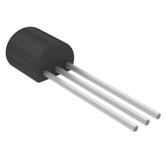
Available in 3-pin TO-92 and 8-pin SOIC low
profile packages
2 Applications
•
•
•
•
Battery chargers
Portable instrumentation
LED lighting
Appliances
See the AN-1112 DSBGA Wafer Level Chip Scale
Package application note for DSBGA considerations.
For more information on the TO-92 package, see the
TO-92
Packing
Options/Ordering
Instructions
application report.
Package Options
DSBGA
8-Pin
1
The LM78Lxx is available in the plastic TO-92 (LP)
package, the SOIC (D) package, and a chip-sized
package (8-Bump DSBGA) using TI's DSBGA
package technology. With adequate heat sinking, the
regulator can deliver 100-mA output current. Current
limiting is included to limit the peak output current to
a safe value. Safe area protection for the output
transistors is provided to limit internal power
dissipation. If internal power dissipation is too high for
the heat sinking provided, the thermal shutdown
circuit prevents the IC from overheating.
Device Information(1)
3
2
PART NUMBER
1
SOIC
8-Pin
BODY SIZE (NOM)
1.30 mm × 1.30 mm
SOIC (8)
3.90 mm × 4.90 mm
TO-92 (3)
3.70 mm × 4.70 mm
(1) For all available packages, see the orderable addendum at
the end of the data sheet.
TO-92
3-Pin
Not to scale
LM78L
PACKAGE
DSBGA (8)
1
Fixed Output Regulator Circuit
1
An IMPORTANT NOTICE at the end of this data sheet addresses availability, warranty, changes, use in safety-critical applications,
intellectual property matters and other important disclaimers. PRODUCTION DATA.
�LM78L
SNVS754L – JANUARY 2000 – REVISED JUNE 2020
www.ti.com
Table of Contents
1
2
3
4
5
6
7
8
Features ..................................................................
Applications ...........................................................
Description .............................................................
Revision History.....................................................
Device Comparison Table.....................................
Pin Configuration and Functions .........................
Specifications.........................................................
1
1
1
2
3
4
5
7.1
7.2
7.3
7.4
7.5
7.6
7.7
7.8
7.9
7.10
5
5
5
5
6
6
7
7
8
9
Absolute Maximum Ratings ......................................
ESD Ratings..............................................................
Recommended Operating Conditions.......................
Thermal Information ..................................................
Electrical Characteristics — LM78L05 ......................
Electrical Characteristics — LM78L09 ......................
Electrical Characteristics — LM78L12 ......................
Electrical Characteristics — LM78L15 ......................
Electrical Characteristics — LM78L62 ......................
Typical Characteristics ............................................
Detailed Description ............................................ 11
8.1 Overview ................................................................. 11
8.2 Functional Block Diagram ....................................... 11
8.3 Feature Description................................................. 12
8.4 Device Functional Modes........................................ 12
9
Application and Implementation ........................ 13
9.1 Application Information............................................ 13
9.2 Typical Applications ................................................ 13
10 Power Supply Recommendations ..................... 16
11 Layout................................................................... 16
11.1 Layout Guidelines ................................................. 16
11.2 Layout Example .................................................... 17
12 Device and Documentation Support ................. 18
12.1
12.2
12.3
12.4
12.5
12.6
Documentation Support ........................................
Receiving Notification of Documentation Updates
Support Resources ...............................................
Trademarks ...........................................................
Electrostatic Discharge Caution ............................
Glossary ................................................................
18
18
18
18
18
18
13 Mechanical, Packaging, and Orderable
Information ........................................................... 18
4 Revision History
NOTE: Page numbers for previous revisions may differ from page numbers in the current version.
Changes from Revision K (December 2016) to Revision L
Page
•
Changed product name to LM78L so document matches product folder .............................................................................. 1
•
Added first Features bullet ..................................................................................................................................................... 1
•
Added Device Comparison Table........................................................................................................................................... 3
Changes from Revision J (December 2013) to Revision K
Page
•
Added Applications section, Device Information table, Pin Configuration and Functions section, ESD Ratings table,
Recommended Operating Conditions table, Detailed Description section, Application and Implementation section,
Power Supply Recommendations section, Layout section, Device and Documentation Support section, and
Mechanical, Packaging, and Orderable Information section .................................................................................................. 1
•
Deleted LM78L82 from the data sheet ................................................................................................................................... 1
•
Added Thermal Information table. .......................................................................................................................................... 1
•
Deleted Lead temperature (soldering) information ................................................................................................................. 5
•
Changed RθJA values for D (SOIC) From: 180 To: 128.8, LP (TO-92) from 230 to 158.7, and YPB (DSBGA) From:
230.9 To 108.4 ....................................................................................................................................................................... 5
•
Changed RθJC values for LP (TO-92) From: 60 To 75.2......................................................................................................... 5
Changes from Revision I (April 2013) to Revision J
•
2
Page
Added the AI suffix ................................................................................................................................................................. 6
Submit Documentation Feedback
Copyright © 2000–2020, Texas Instruments Incorporated
Product Folder Links: LM78L
�LM78L
www.ti.com
SNVS754L – JANUARY 2000 – REVISED JUNE 2020
5 Device Comparison Table
IOUT
PARAMETER
LM78xx
UA78
LM340
LM340A
UNIT
Input voltage range
7 - 35
7 - 38
7 - 35
7 - 35
V
5, 12, 15
5, 8, 10, 12, 15,
24
5, 12, 15
5, 12, 15
V
Fixed output voltage option
1.5 A
Load regulation accuracy
4
4
4
2
%
PSRR (120 Hz)
80
78
80
80
dB
Recommended operating temperature
0 - 125
0 - 125
0 - 125
0 - 125
°C
TO-220 TJA
23.9
19
23.9
23.9
°C/W
SOT-223 TJA
62.1
N/A
62.1
62.1
°C/W
TO-3 TJA
39
N/A
39
39
°C/W
°C/W
TO-263 TJA
0.5 A
44.8
25.3
44.8
44.8
LM78Mxx
UA78MxxC
UA78MxxI
LM341
Input voltage range
7.2 - 35
5.3 - 30
5.3 - 30
7.2 - 35
V
Fixed output voltage option
5
3.3, 5, 6, 8, 9,
10, 12
3.3, 5
5
V
Load regulation accuracy
4
3
3
4
%
PSRR (120 Hz)
78
80
80
78
dB
Recommended operating temperature
–40 - 125
0 - 125
–40 - 125
–40 - 125
°C
TO-220 TJA
22.6
19
19
22.6
°C/W
SOT-223 TJA
N/A
53
53
N/A
°C/W
TO-3 TJA
162.4
N/A
N/A
N/A
°C/W
TO-252 Powerflex TJA
N/A
28
28
N/A
°C/W
TO-252 TJA
38
30.3
30.3
N/A
°C/W
LM78LxxAC
LM78LxxAI,
LM78LxxIT
UA78LxxC
UA78LxxI
7.0 - 30
7.0 - 30
4.75 - 30
4.75 - 30
V
5, 9
2.6, 5, 6.2, 8, 9,
10, 12, 15
5
V
Input voltage range
Fixed output voltage option
0.1 A
5, 6.2, 12, 15
Load regulation accuracy (A/non -A)
4
4
4, 8
4, 8
%
PSRR (120 Hz)
62
62
51
51
dB
Recommended operating temperature
0 - 125
–40 - 125
0 - 125
–40 - 125
°C
SOT-89 TJA
N/A
N/A
54.7
54.7
°C/W
SO-8 TJA
128.8
128.8
115
115
°C/W
DSBGA TJA
N/A
108.4
N/A
N/A
°C/W
TO-92 TJA
158.7
N/A
143.6
143.6
°C/W
Submit Documentation Feedback
Copyright © 2000–2020, Texas Instruments Incorporated
Product Folder Links: LM78L
3
�LM78L
SNVS754L – JANUARY 2000 – REVISED JUNE 2020
www.ti.com
6 Pin Configuration and Functions
YPB Package
8-Pin DSBGA
Top View
A
3
2
D Package
8-Pin SOIC
Top View
B
VOUT
C
NC
VOUT
1
8
VIN
GND
2
7
GND
GND
3
6
GND
NC
4
5
NC
GND
VOUT
GND
Not to scale
1
VIN
VIN
NC
Not to scale
LP Package
3-Pin TO-92
Bottom View
3
VIN
2
GND
1
VOUT
Not to scale
Pin Functions
PIN
DESCRIPTION
DSBGA
SOIC
GND
C2, C3
2, 3, 6, 7
2
—
Ground
NC
B3, C1
4, 5
—
—
No connection
VIN
A1, B1
8
3
I
Input supply voltage pin
VOUT
A2, A3
1
1
O
Output voltage pin
4
TO-92
I/O
NAME
Submit Documentation Feedback
Copyright © 2000–2020, Texas Instruments Incorporated
Product Folder Links: LM78L
�LM78L
www.ti.com
SNVS754L – JANUARY 2000 – REVISED JUNE 2020
7 Specifications
7.1 Absolute Maximum Ratings
over operating free-air temperature range (unless otherwise noted) (1) (2)
MIN
MAX
UNIT
35
V
Input voltage
Power dissipation
Internally limited
Operating junction temperature, TJ
LM78LxxACZ (TO-92)
0
125
LM78LxxACM (SOIC)
0
125
LM78LxxAIM (SOIC)
–40
125
LM78LxxITP (thin DSBGA)
–40
85
–65
150
Storage temperature, Tstg
(1)
(2)
°C
°C
Stresses beyond those listed under Absolute Maximum Ratings may cause permanent damage to the device. These are stress ratings
only, which do not imply functional operation of the device at these or any other conditions beyond those indicated under Recommended
Operating Conditions. Exposure to absolute-maximum-rated conditions for extended periods may affect device reliability.
If Military/Aerospace specified devices are required, please contact the Texas Instruments Sales Office/Distributors for availability and
specifications.
7.2 ESD Ratings
V(ESD)
(1)
Electrostatic discharge
Human-body model (HBM),
VALUE
UNIT
±1000
V
(1)
Human body model, 1.5 kΩ in series with 100 pF.
7.3 Recommended Operating Conditions
over operating free-air temperature range (unless otherwise noted)
MIN
NOM
Input voltage
Continuous output current
LM78LxxACZ (TO-92)
TJ
LM78LxxACM (SOIC)
Junction temperature
MAX
UNIT
30
V
100
mA
0
125
0
125
LM78LxxAIM (SOIC)
–40
125
LM78LxxITP (DSBGA)
–40
85
°C
7.4 Thermal Information
LM78Lxx
THERMAL METRIC
(1)
D (SOIC)
LP (TO-92)
YPB (DSBGA)
8 PINS
3 PINS
8 PINS
UNIT
128.8
158.7
108.4
°C/W
RθJA
Junction-to-ambient thermal resistance
RθJC(top)
Junction-to-case (top) thermal resistance
76
75.2
1.3
°C/W
RθJB
Junction-to-board thermal resistance
69.3
n/a
31.4
°C/W
ψJT
Junction-to-top characterization parameter
26.3
30.2
4.5
°C/W
ψJB
Junction-to-board characterization parameter
68.8
138.2
31.4
°C/W
RθJC(bot)
Junction-to-case (bottom) thermal resistance
—
—
—
°C/W
(1)
For more information about traditional and new thermal metrics, see the Semiconductor and IC Package Thermal Metrics application
report.
Submit Documentation Feedback
Copyright © 2000–2020, Texas Instruments Incorporated
Product Folder Links: LM78L
5
�LM78L
SNVS754L – JANUARY 2000 – REVISED JUNE 2020
www.ti.com
7.5 Electrical Characteristics — LM78L05
Typical values apply for TJ = 25°C, Minimum and Maximum limits apply for the entire operating temperature range of the
package (1) (2), IO = 40 mA, CI = 0.33 µF, CO = 0.1 µF, VIN = 10 V (unless otherwise noted).
PARAMETER
TEST CONDITIONS
TJ = 25°C
VO
Output voltage
Line regulation
ΔVO
Load regulation
IQ
Quiescent current
ΔIQ
Quiescent current change
Vn
Output noise voltage
ΔVIN/ΔVO Ripple rejection
MIN
TYP
MAX
4.8
5
5.2
VIN = 7 V to 20 V, IO = 1 mA to 40 mA (3)
4.75
5.25
IO = 1 mA to 70 mA (3)
4.75
5.25
VIN = 7 V to 20 V, TJ = 25°C
18
75
VIN = 8 V to 20 V, TJ = 25°C
10
54
IO = 1 mA to 100 mA, TJ = 25°C
20
60
IO = 1 mA to 40 mA, TJ = 25°C
5
30
TJ = 25°C
3
5
VIN = 8 V to 20 V
V
mV
mA
1
IO = 1 mA to 40 mA
mA
0.1
f = 10 Hz to 100 kHz (4)
40
f = 120 Hz, VIN = 8 V to 16 V, TJ = 25°C
47
µV
62
dB
140
mA
IPK
Peak output current
ΔVO/ΔT
Average output voltage temperature
coefficient
IO = 5 mA
–0.65
VIN(MIN)
Minimum value of input voltage
required to maintain line regulation
TJ = 25°C
6.7
(1)
(2)
(3)
(4)
UNIT
mV/°C
7
V
For the operating ranges of each package, see Absolute Maximum Ratings.
Limits are ensured by production testing or correlation techniques using standard Statistical Quality Control (SQC) methods.
Power dissipation ≤ 0.75 W.
Recommended minimum load capacitance of 0.01 µF to limit high-frequency noise.
7.6 Electrical Characteristics — LM78L09
Typical values apply for TJ = 25°C, Minimum and Maximum limits apply for the entire operating temperature range of the
package (1) (2), IO = 40 mA, CI = 0.33 µF, CO = 0.1 µF, VIN = 15 V (unless otherwise noted).
PARAMETER
VO
Output voltage
Line regulation
ΔVO
Load regulation
IQ
Quiescent current
ΔIQ
Quiescent current change
Vn
Output noise voltage
ΔVIN/ΔVO Ripple rejection
IPK
Peak output current
ΔVO/ΔT
Average output voltage temperature
coefficient
VIN(MIN)
Minimum value of input voltage
required to maintain line regulation
(1)
(2)
(3)
6
TEST CONDITIONS
MIN
TYP
MAX
TJ = 25°C
8.64
9
9.36
VIN = 11.5 V to 24 V, IO = 1 mA to 40 mA (3)
8.55
9.45
IO = 1 mA to 70 mA (3)
8.55
9.45
VIN = 11.5 V to 24 V, TJ = 25°C
100
200
VIN = 13 V to 24 V, TJ = 25°C
90
150
IO = 1 mA to 100 mA, TJ = 25°C
20
90
IO = 1 mA to 40 mA, TJ = 25°C
10
45
2
5.5
TJ = 25°C
VIN = 11.5 V to 24 V
1.5
IO = 1 mA to 40 mA
0.1
70
f = 120 Hz, VIN = 15 V to 25 V, TJ = 25°C
IO = 5 mA
38
UNIT
V
mV
mA
mA
µV
44
dB
140
mA
–0.9
mV/°C
10.7
V
For the operating ranges of each package, see Absolute Maximum Ratings.
Limits are ensured by production testing or correlation techniques using standard Statistical Quality Control (SQC) methods.
Power dissipation ≤ 0.75 W.
Submit Documentation Feedback
Copyright © 2000–2020, Texas Instruments Incorporated
Product Folder Links: LM78L
�LM78L
www.ti.com
SNVS754L – JANUARY 2000 – REVISED JUNE 2020
7.7 Electrical Characteristics — LM78L12
Typical values apply for TJ = 25°C, Minimum and Maximum limits apply for the entire operating temperature range of the
package (1) (2), IO = 40 mA, CI = 0.33 µF, CO = 0.1 µF, VIN = 19 V (unless otherwise noted).
PARAMETER
VO
Output voltage
Line regulation
ΔVO
Load regulation
IQ
Quiescent current
ΔIQ
Quiescent current change
Vn
Output noise voltage
ΔVIN/ΔVO Ripple rejection
IPK
Peak output current
ΔVO/ΔT
Average output voltage temperature
coefficient
VIN(MIN)
Minimum value of input voltage
required to maintain line regulation
(1)
(2)
(3)
MIN
TYP
MAX
TJ = 25°C
TEST CONDITIONS
11.5
12
12.5
VIN = 14.5 V to 27 V, IO = 1 mA to 40 mA (3)
11.4
12.6
IO = 1 mA to 70 mA (3)
11.4
12.6
VIN = 14.5 V to 27 V, TJ = 25°C
30
180
VIN = 16 V to 27 V, TJ = 25°C
20
110
IO = 1 mA to 100 mA, TJ = 25°C
30
100
IO = 1 mA to 40 mA, TJ = 25°C
10
50
3
5
TJ = 25°C
VIN = 16 V to 27 V
UNIT
V
mV
mA
1
IO = 1 mA to 40 mA
mA
0.1
80
f = 120 Hz, VIN = 15 V to 25 V, TJ = 25°C
40
µV
54
dB
140
mA
IO = 5 mA
–1
mV/°C
TJ = 25°C
13.7
14.5
V
For the operating ranges of each package, see Absolute Maximum Ratings.
Limits are ensured by production testing or correlation techniques using standard Statistical Quality Control (SQC) methods.
Power dissipation ≤ 0.75 W.
7.8 Electrical Characteristics — LM78L15
Typical values apply for TJ = 25°C, Minimum and Maximum limits apply for the entire operating temperature range of the
package (1) (2), IO = 40 mA, CI = 0.33 µF, CO = 0.1 µF, VIN = 23 V (unless otherwise noted).
PARAMETER
TEST CONDITIONS
TJ = 25°C
VO
Output voltage
Line regulation
ΔVO
Load regulation
IQ
Quiescent current
ΔIQ
Quiescent current change
Vn
Output noise voltage
ΔVIN/ΔVO Ripple rejection
IPK
Peak output current
ΔVO/ΔT
Average output voltage temperature
coefficient
VIN(MIN)
Minimum value of input voltage
required to maintain line regulation
(1)
(2)
(3)
MIN
TYP
MAX
14.4
15
15.6
VIN = 17.5 V to 30 V, IO = 1 mA to 40 mA (3)
14.25
15.75
IO = 1 mA to 70 mA (3)
14.25
15.75
VIN = 17.5 V to 30 V, TJ = 25°C
37
250
VIN = 20 V to 30 V, TJ = 25°C
25
140
IO = 1 mA to 100 mA, TJ = 25°C
35
150
IO = 1 mA to 40 mA, TJ = 25°C
12
75
3
5
TJ = 25°C
VIN =20 V to 30 V
1
IO = 1 mA to 40 mA
0.1
90
f = 120 Hz, VIN = 18.5 V to 28.5 V, TJ = 25°C
37
UNIT
V
mV
mA
mA
µV
51
dB
140
mA
IO = 5 mA
–1.3
mV/°C
TJ = 25°C
16.7
17.5
V
For the operating ranges of each package, see Absolute Maximum Ratings.
Limits are ensured by production testing or correlation techniques using standard Statistical Quality Control (SQC) methods.
Power dissipation ≤ 0.75 W.
Submit Documentation Feedback
Copyright © 2000–2020, Texas Instruments Incorporated
Product Folder Links: LM78L
7
�LM78L
SNVS754L – JANUARY 2000 – REVISED JUNE 2020
www.ti.com
7.9 Electrical Characteristics — LM78L62
Typical values apply for TJ = 25°C, Minimum and Maximum limits apply for the entire operating temperature range of the
package (1) (2), IO = 40 mA, CI = 0.33 µF, CO = 0.1 µF, VIN = 12 V (unless otherwise noted).
PARAMETER
TEST CONDITIONS
TJ = 25°C
VO
Output voltage
Line regulation
ΔVO
Load regulation
IQ
Quiescent current
ΔIQ
Quiescent current change
Vn
Output noise voltage
ΔVIN/ΔVO Ripple rejection
IPK
Peak output current
ΔVO/ΔT
Average output voltage temperature
coefficient
VIN(MIN)
Minimum value of input voltage
required to maintain line regulation
(1)
(2)
(3)
(4)
8
MIN
TYP
MAX
5.95
6.2
6.45
VIN = 8.5 V to 20 V, IO = 1 mA to 40 mA (3)
5.9
6.5
IO = 1 mA to 70 mA (3)
5.9
6.5
VIN = 8.5 V to 20 V, TJ = 25°C
65
175
VIN = 9 V to 20 V, TJ = 25°C
55
125
IO = 1 mA to 100 mA, TJ = 25°C
13
80
IO = 1 mA to 40 mA, TJ = 25°C
6
40
TJ = 25°C
2
5.5
VIN = 8 V to 20 V
1.5
IO = 1 mA to 40 mA
0.1
f = 10 Hz to 100 kHz (4)
50
f = 120 Hz, VIN = 10 V to 20 V, TJ = 25°C
IO = 5 mA
40
UNIT
V
mV
mA
mA
µV
46
dB
140
mA
–0.75
7.9
mV/°C
V
For the operating ranges of each package, see Absolute Maximum Ratings.
Limits are ensured by production testing or correlation techniques using standard Statistical Quality Control (SQC) methods.
Power dissipation ≤ 0.75 W.
Recommended minimum load capacitance of 0.01 µF to limit high-frequency noise.
Submit Documentation Feedback
Copyright © 2000–2020, Texas Instruments Incorporated
Product Folder Links: LM78L
�LM78L
www.ti.com
SNVS754L – JANUARY 2000 – REVISED JUNE 2020
7.10 Typical Characteristics
LP Package
Figure 1. Maximum Average Power Dissipation
Figure 2. Peak Output Current
Figure 3. Dropout Voltage
Figure 4. Ripple Rejection
Figure 5. Output Impedance
Figure 6. Quiescent Current
Submit Documentation Feedback
Copyright © 2000–2020, Texas Instruments Incorporated
Product Folder Links: LM78L
9
�LM78L
SNVS754L – JANUARY 2000 – REVISED JUNE 2020
www.ti.com
Typical Characteristics (continued)
Figure 7. Quiescent Current
10
Submit Documentation Feedback
Copyright © 2000–2020, Texas Instruments Incorporated
Product Folder Links: LM78L
�LM78L
www.ti.com
SNVS754L – JANUARY 2000 – REVISED JUNE 2020
8 Detailed Description
8.1 Overview
The LM78Lxx series of positive regulators is available in the following fixed output voltages: 5 V, 6.2 V, 8.2 V,
9 V, 12 V, and 15 V. The regulator can be configured to an adjustable output by connecting the GND pin to the
center of a resistive voltage divider as shown in Figure 10. In this configuration, the fixed output voltage acts as
the reference voltage across R1 allowing the output to be adjusted by changing the resistor.
8.2 Functional Block Diagram
Submit Documentation Feedback
Copyright © 2000–2020, Texas Instruments Incorporated
Product Folder Links: LM78L
11
�LM78L
SNVS754L – JANUARY 2000 – REVISED JUNE 2020
www.ti.com
8.3 Feature Description
8.3.1 Load Regulation
These devices regulate the voltage between the VOUT and GND pins, and can be made adjustable by using a
resistive voltage divider. The output voltage tolerance is ±5% over temperature.
8.3.2 Protection
The LM78Lxx series of regulators has internal thermal overload protection that automatically shuts off the device
if the operating temperature becomes too high. There is also internal short-circuit current limit and output
transistor safe area protection that shuts down the device if the output current becomes too high.
8.4 Device Functional Modes
8.4.1 Normal Operation
The VOUT pin sources current necessary to set the voltage on VOUT at a fixed voltage above the GND pin. See
Specifications for VO of each device.
8.4.2 Shutdown
The device automatically shuts down if the output current or its internal temperature becomes too high.
12
Submit Documentation Feedback
Copyright © 2000–2020, Texas Instruments Incorporated
Product Folder Links: LM78L
�LM78L
www.ti.com
SNVS754L – JANUARY 2000 – REVISED JUNE 2020
9 Application and Implementation
NOTE
Information in the following applications sections is not part of the TI component
specification, and TI does not warrant its accuracy or completeness. TI’s customers are
responsible for determining suitability of components for their purposes. Customers should
validate and test their design implementation to confirm system functionality.
9.1 Application Information
These devices are versatile and high-performance regulators with a wide temperature range and tight line and
load regulation. An input capacitor is required if the regulator is placed more than 3 inches from the power supply
filter. TI recommends a minimum load capacitance of 0.01 µF to limit high frequency.
9.2 Typical Applications
9.2.1 Fixed Output Regulator
*Required if the regulator is located more than 3 inches from the power supply filter.
**Recommended minimum load capacitance of 0.01 µF to limit high-frequency noise.
Figure 8. Fixed Output Regulator Circuit
9.2.1.1 Design Requirements
The device component count is very minimal. No external components are usually required. However, TI
recommends input or output capacitors depending on the distance between the device and the power supply and
if extra filtering is needed at the output.
The output voltage is set based on the selection of the two resistors (R1 and R2), as shown in Figure 14.
9.2.1.2 Detailed Design Procedure
9.2.1.2.1 Input Capacitor
An input capacitor is required if the regulator is placed more than 3 inches from the power supply filter. A 0.33-µF
capacitor on the input is suitable for most applications.
9.2.1.2.2 Output Capacitor
TI recommends a minimum load capacitance of 0.01 µF to limit high-frequency noise.
Submit Documentation Feedback
Copyright © 2000–2020, Texas Instruments Incorporated
Product Folder Links: LM78L
13
�LM78L
SNVS754L – JANUARY 2000 – REVISED JUNE 2020
www.ti.com
Typical Applications (continued)
9.2.1.3 Application Curve
Input - Output Differential (V)
1.9
1.8
1.7
1.6
1.5
1.4
1.3
25qC
1.2
0
20
40
60
Load Current (mA)
80
100
Figure 9. LM78Lxx Dropout
9.2.2 Other Application Circuits
Figure 10 to Figure 14 show application circuit examples using the LM78Lxx devices. Customers must fully
validate and test these circuits before implementing a design based on these examples. Unless otherwise noted,
the design procedures in Fixed Output Regulator are applicable to these designs.
VO = 5 V + (5 V / R1 + IQ) × R2*
* The 5 V represents the fixed output voltage of the LM78L05. If using one of the other LM78Lxx devices, use that
fixed output voltage value when calculating VO.
IQ < 5 V / (3 × R1)
Load regulation (LR) of LM78L05 ≈ (R1 + R2) / R1
Figure 10. Adjustable Output Regulator Circuit
14
Submit Documentation Feedback
Copyright © 2000–2020, Texas Instruments Incorporated
Product Folder Links: LM78L
�LM78L
www.ti.com
SNVS754L – JANUARY 2000 – REVISED JUNE 2020
Typical Applications (continued)
IOUT = (VO / R1) + IQ
IQ = 1.5 mA over line and load changes
Figure 11. Current Regulator Circuit
*Solid tantalum
**Heat sink Q1
***Optional: Improves ripple rejection and transient response.
Load Regulation = 0.6%, IL = 0 mA to 250 mA pulsed with tON = 50 ms.
Figure 12. 5-V, 500-mA Regulator With Short-Circuit Protection Circuit
*Solid tantalum
Figure 13. ±15-V, 100-mA Dual Power Supply Circuit
Submit Documentation Feedback
Copyright © 2000–2020, Texas Instruments Incorporated
Product Folder Links: LM78L
15
�LM78L
SNVS754L – JANUARY 2000 – REVISED JUNE 2020
www.ti.com
Typical Applications (continued)
*Solid tantalum
VO = VG + 5 V, R1 = (–VIN / IQ(LM78L05))
VO = 5 V (R2 / R4) for (R2 + R3) = (R4 + R5)
A 0.5-V output will correspond to (R2 / R4) = 0.1, (R3 / R4) = 0.9
Figure 14. Variable Output Regulator Circuit (0.5 V to 18 V)
10 Power Supply Recommendations
The linear regulator input supply must be well regulated and kept at a voltage level to not exceed the maximum
input to output voltage differential allowed by the device. The minimum dropout voltage (VIN – VO) must be met
with extra headroom when possible to keep the output well regulated. A 0.33-µF or higher capacitor must be
placed at the input to bypass noise.
11 Layout
11.1 Layout Guidelines
For the best overall performance, some layout guidelines may be disregarded. Place all circuit components on
the same side of the circuit board and as near as practical to the respective linear regulator pins. Traces must be
kept short and wide to reduce the amount of parasitic elements in the system. The actual width and thickness of
traces depends on the current carrying capability and heat dissipation required by the end system.
16
Submit Documentation Feedback
Copyright © 2000–2020, Texas Instruments Incorporated
Product Folder Links: LM78L
�LM78L
www.ti.com
SNVS754L – JANUARY 2000 – REVISED JUNE 2020
11.2 Layout Example
GND
U1
C1
C2
VOUT
VIN
Figure 15. LM78Lxx Example Circuit Layout
Submit Documentation Feedback
Copyright © 2000–2020, Texas Instruments Incorporated
Product Folder Links: LM78L
17
�LM78L
SNVS754L – JANUARY 2000 – REVISED JUNE 2020
www.ti.com
12 Device and Documentation Support
12.1 Documentation Support
12.1.1 Related Documentation
For related documentation see the following:
• Texas Instruments, UA78L00 Series Positive-Voltage Linear Regulators data sheet
• Texas Instruments, AN-1112 DSBGA Wafer Level Chip Scale Package application note
• Texas Instruments, TO-92 Packing Options/Ordering Instructions application report
12.2 Receiving Notification of Documentation Updates
To receive notification of documentation updates, navigate to the device product folder on ti.com. In the upper
right corner, click on Alert me to register and receive a weekly digest of any product information that has
changed. For change details, review the revision history included in any revised document.
12.3 Support Resources
TI E2E™ support forums are an engineer's go-to source for fast, verified answers and design help — straight
from the experts. Search existing answers or ask your own question to get the quick design help you need.
Linked content is provided "AS IS" by the respective contributors. They do not constitute TI specifications and do
not necessarily reflect TI's views; see TI's Terms of Use.
12.4 Trademarks
E2E is a trademark of Texas Instruments.
All other trademarks are the property of their respective owners.
12.5 Electrostatic Discharge Caution
This integrated circuit can be damaged by ESD. Texas Instruments recommends that all integrated circuits be handled with
appropriate precautions. Failure to observe proper handling and installation procedures can cause damage.
ESD damage can range from subtle performance degradation to complete device failure. Precision integrated circuits may be more
susceptible to damage because very small parametric changes could cause the device not to meet its published specifications.
12.6 Glossary
SLYZ022 — TI Glossary.
This glossary lists and explains terms, acronyms, and definitions.
13 Mechanical, Packaging, and Orderable Information
The following pages include mechanical, packaging, and orderable information. This information is the most
current data available for the designated devices. This data is subject to change without notice and revision of
this document. For browser-based versions of this data sheet, refer to the left-hand navigation.
18
Submit Documentation Feedback
Copyright © 2000–2020, Texas Instruments Incorporated
Product Folder Links: LM78L
�PACKAGE OPTION ADDENDUM
www.ti.com
4-Aug-2022
PACKAGING INFORMATION
Orderable Device
Status
(1)
Package Type Package Pins Package
Drawing
Qty
Eco Plan
(2)
Lead finish/
Ball material
MSL Peak Temp
Op Temp (°C)
Device Marking
(3)
Samples
(4/5)
(6)
LM78L05ACM
NRND
SOIC
D
8
95
Non-RoHS
& Green
Call TI
Level-1-235C-UNLIM
0 to 125
LM78L
05ACM
LM78L05ACM/NOPB
ACTIVE
SOIC
D
8
95
RoHS & Green
SN
Level-1-260C-UNLIM
0 to 125
LM78L
05ACM
LM78L05ACMX
NRND
SOIC
D
8
2500
Non-RoHS
& Green
Call TI
Level-1-235C-UNLIM
0 to 125
LM78L
05ACM
LM78L05ACMX/NOPB
ACTIVE
SOIC
D
8
2500
RoHS & Green
SN
Level-1-260C-UNLIM
0 to 125
LM78L
05ACM
Samples
LM78L05ACZ/LFT1
ACTIVE
TO-92
LP
3
2000
RoHS & Green
SN
N / A for Pkg Type
0 to 125
LM78L
05ACZ
Samples
LM78L05ACZ/LFT3
ACTIVE
TO-92
LP
3
2000
RoHS & Green
SN
N / A for Pkg Type
0 to 125
LM78L
05ACZ
Samples
LM78L05ACZ/LFT4
ACTIVE
TO-92
LP
3
2000
RoHS & Green
SN
N / A for Pkg Type
0 to 125
LM78L
05ACZ
Samples
LM78L05ACZ/LFT7
ACTIVE
TO-92
LP
3
2000
RoHS & Green
SN
N / A for Pkg Type
0 to 125
LM78L
05ACZ
Samples
LM78L05ACZ/NOPB
ACTIVE
TO-92
LP
3
1800
RoHS & Green
Call TI
N / A for Pkg Type
0 to 125
LM78L
05ACZ
Samples
LM78L05AIM/NOPB
ACTIVE
SOIC
D
8
95
RoHS & Green
SN
Level-1-260C-UNLIM
-40 to 125
LM78L
05AM
Samples
LM78L05AIMX/NOPB
ACTIVE
SOIC
D
8
2500
RoHS & Green
SN
Level-1-260C-UNLIM
-40 to 125
LM78L
05AM
Samples
LM78L05ITP/NOPB
ACTIVE
DSBGA
YPB
8
250
RoHS & Green
SNAGCU
Level-1-260C-UNLIM
-40 to 85
P
03
Samples
LM78L05ITPX/NOPB
ACTIVE
DSBGA
YPB
8
3000
RoHS & Green
SNAGCU
Level-1-260C-UNLIM
-40 to 85
P
03
Samples
LM78L09ITPX/NOPB
ACTIVE
DSBGA
YPB
8
3000
RoHS & Green
SNAGCU
Level-1-260C-UNLIM
-40 to 85
P
02
Samples
LM78L12ACM
NRND
SOIC
D
8
95
Non-RoHS
& Green
Call TI
Level-1-235C-UNLIM
0 to 125
LM78L
12ACM
LM78L12ACM/NOPB
ACTIVE
SOIC
D
8
95
RoHS & Green
SN
Level-1-260C-UNLIM
0 to 125
LM78L
12ACM
Samples
LM78L12ACMX/NOPB
ACTIVE
SOIC
D
8
2500
RoHS & Green
SN
Level-1-260C-UNLIM
0 to 125
LM78L
Samples
Addendum-Page 1
Samples
�PACKAGE OPTION ADDENDUM
www.ti.com
Orderable Device
4-Aug-2022
Status
(1)
Package Type Package Pins Package
Drawing
Qty
Eco Plan
(2)
Lead finish/
Ball material
MSL Peak Temp
Op Temp (°C)
Device Marking
(3)
Samples
(4/5)
(6)
12ACM
LM78L12ACZ/LFT3
ACTIVE
TO-92
LP
3
2000
RoHS & Green
SN
N / A for Pkg Type
0 to 125
LM78L
12ACZ
Samples
LM78L12ACZ/LFT4
ACTIVE
TO-92
LP
3
2000
RoHS & Green
SN
N / A for Pkg Type
0 to 125
LM78L
12ACZ
Samples
LM78L12ACZ/LFT7
ACTIVE
TO-92
LP
3
2000
RoHS & Green
SN
N / A for Pkg Type
0 to 125
LM78L
12ACZ
Samples
LM78L12ACZ/NOPB
ACTIVE
TO-92
LP
3
1800
RoHS & Green
SN
N / A for Pkg Type
0 to 125
LM78L
12ACZ
Samples
LM78L15ACM
NRND
SOIC
D
8
95
Non-RoHS
& Green
Call TI
Level-1-235C-UNLIM
0 to 125
LM78L
15ACM
LM78L15ACM/NOPB
ACTIVE
SOIC
D
8
95
RoHS & Green
SN
Level-1-260C-UNLIM
0 to 125
LM78L
15ACM
LM78L15ACMX
NRND
SOIC
D
8
2500
Non-RoHS
& Green
Call TI
Level-1-235C-UNLIM
0 to 125
LM78L
15ACM
LM78L15ACMX/NOPB
ACTIVE
SOIC
D
8
2500
RoHS & Green
SN
Level-1-260C-UNLIM
0 to 125
LM78L
15ACM
Samples
LM78L15ACZ/LFT4
ACTIVE
TO-92
LP
3
2000
RoHS & Green
SN
N / A for Pkg Type
0 to 125
LM78L
15ACZ
Samples
LM78L15ACZ/NOPB
ACTIVE
TO-92
LP
3
1800
RoHS & Green
SN
N / A for Pkg Type
0 to 125
LM78L
15ACZ
Samples
LM78L62ACZ/NOPB
ACTIVE
TO-92
LP
3
1800
RoHS & Green
SN
N / A for Pkg Type
0 to 125
LM78L
62ACZ
Samples
(1)
The marketing status values are defined as follows:
ACTIVE: Product device recommended for new designs.
LIFEBUY: TI has announced that the device will be discontinued, and a lifetime-buy period is in effect.
NRND: Not recommended for new designs. Device is in production to support existing customers, but TI does not recommend using this part in a new design.
PREVIEW: Device has been announced but is not in production. Samples may or may not be available.
OBSOLETE: TI has discontinued the production of the device.
(2)
RoHS: TI defines "RoHS" to mean semiconductor products that are compliant with the current EU RoHS requirements for all 10 RoHS substances, including the requirement that RoHS substance
do not exceed 0.1% by weight in homogeneous materials. Where designed to be soldered at high temperatures, "RoHS" products are suitable for use in specified lead-free processes. TI may
reference these types of products as "Pb-Free".
RoHS Exempt: TI defines "RoHS Exempt" to mean products that contain lead but are compliant with EU RoHS pursuant to a specific EU RoHS exemption.
Green: TI defines "Green" to mean the content of Chlorine (Cl) and Bromine (Br) based flame retardants meet JS709B low halogen requirements of


 工商网监
湘ICP备2023018690号
工商网监
湘ICP备2023018690号
