LM828
www.ti.com
SNOS035D – MARCH 2010 – REVISED MAY 2013
LM828 Switched Capacitor Voltage Converter
Check for Samples: LM828
FEATURES
DESCRIPTION
•
•
•
•
The LM828 CMOS charge-pump voltage converter
inverts a positive voltage in the range of +1.8V to
+5.5V to the corresponding negative voltage of −1.8V
to −5.5V. The LM828 uses two low cost capacitors to
provide up to 25 mA of output current.
1
2
Inverts Input Supply Voltage
SOT-23 Package
20Ω Typical Output Impedance
97% Typical Conversion Efficiency at 5 mA
APPLICATIONS
•
•
•
•
•
•
Cellular Phones
Pagers
PDAs
Operational Amplifier Power Supplies
Interface Power Supplies
Handheld Instruments
The LM828 operates at 12 kHz switching frequency
to reduce output resistance and voltage ripple. With
an operating current of only 40 µA (operating
efficiency greater than 96% with most loads), the
LM828 provides ideal performance for battery
powered systems. The device is in a tiny SOT-23
package.
Basic Application Circuits
Voltage Inverter
+5V to −10V Converter
1
2
Please be aware that an important notice concerning availability, standard warranty, and use in critical applications of
Texas Instruments semiconductor products and disclaimers thereto appears at the end of this data sheet.
All trademarks are the property of their respective owners.
PRODUCTION DATA information is current as of publication date.
Products conform to specifications per the terms of the Texas
Instruments standard warranty. Production processing does not
necessarily include testing of all parameters.
Copyright © 2010–2013, Texas Instruments Incorporated
�LM828
SNOS035D – MARCH 2010 – REVISED MAY 2013
www.ti.com
These devices have limited built-in ESD protection. The leads should be shorted together or the device placed in conductive foam
during storage or handling to prevent electrostatic damage to the MOS gates.
Absolute Maximum Ratings (1) (2)
Supply Voltage (V+ to GND, or GND to OUT)
5.8V
V+ and OUT Continuous Output Current
50 mA
Output Short-Circuit Duration to GND (3)
Continuous Power Dissipation (TA = 25°C)
1 sec.
(4)
240 mW
TJMax (4)
150°C
θJA (4)
300°C/W
−40°C to 85°C
Operating Junction Temperature Range
−65°C to +150°C
Storage Temperature Range
Lead Temp. (Soldering, 10 seconds)
ESD Rating
(1)
300°C
(5)
2kV
Absolute maximum ratings indicate limits beyond which damage to the device may occur. Electrical specifications do not apply when
operating the device beyond its rated operating conditions.
If Military/Aerospace specified devices are required, please contact the Texas Instruments Sales Office/Distributors for availability and
specifications.
OUT may be shorted to GND for one second without damage. However, shorting OUT to V+ may damage the device and should be
avoided. Also, for temperatures above 85°C, OUT must not be shorted to GND or V+, or the device may be damaged.
The maximum allowable power dissipation is calculated by using PDMax = (TJMax − TA)/θJA, where TJMax is the maximum junction
temperature, TA is the ambient temperature, and θJA is the junction-to-ambient thermal resistance of the package.
The human body model is a 100 pF capacitor discharged through a 1.5 kΩ resistor into each pin.
(2)
(3)
(4)
(5)
Electrical Characteristics
Limits in standard typeface are for TJ = 25°C, and limits in boldface type apply over the full operating temperature range.
Unless otherwise specified: V+ = 5V, C1 = C2 = 10 μF. (1)
Condition
Min
V+
Symbol
Supply Voltage
Parameter
RL =10kΩ
1.8
IQ
Supply Current
No Load
Typ
40
Max
Units
5.5
V
75
µA
115
ROUT
Output Resistance (2)
IL = 5 mA
(3)
20
65
Ω
fOSC
Oscillator Frequency
Internal
12
24
56
kHz
fSW
Switching Frequency (3)
Measured at CAP+
6
12
28
kHz
PEFF
Power Efficiency
IL = 5 mA
VOEFF
Voltage Conversion Efficiency
No Load
(1)
(2)
(3)
2
95
97
%
99.96
%
In the test circuit, capacitors C1 and C2 are 10 µF, 0.3Ω maximum ESR capacitors. Capacitors with higher ESR will increase output
resistance, reduce output voltage and efficiency.
Specified output resistance includes internal switch resistance and capacitor ESR. See the details in the application information.
The output switches operate at one half of the oscillator frequency, fOSC = 2fSW.
Submit Documentation Feedback
Copyright © 2010–2013, Texas Instruments Incorporated
Product Folder Links: LM828
�LM828
www.ti.com
SNOS035D – MARCH 2010 – REVISED MAY 2013
Test Circuit
*C1 and C2 are 10 µF capacitors.
Figure 1. LM828 Test Circuit
Typical Performance Characteristics
(Circuit of Figure 1, V+ = 5V unless otherwise specified)
Supply Current vs
Supply Voltage
Supply Current vs
Temperature
Figure 2.
Figure 3.
Output Source Resistance
vs
Supply Voltage
Output Source Resistance
vs
Temperature
Figure 4.
Figure 5.
Submit Documentation Feedback
Copyright © 2010–2013, Texas Instruments Incorporated
Product Folder Links: LM828
3
�LM828
SNOS035D – MARCH 2010 – REVISED MAY 2013
www.ti.com
Typical Performance Characteristics (continued)
(Circuit of Figure 1, V+ = 5V unless otherwise specified)
Output Voltage
vs Load Current
Efficiency vs
Load Current
Figure 6.
Figure 7.
Switching Frequency vs
Supply Voltage
Switching Frequency vs
Temperature
Figure 8.
Figure 9.
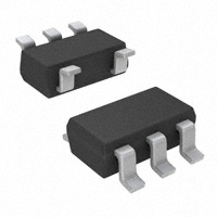
CONNECTION DIAGRAMS
5-Lead SOT-23 Package (DBV)
Figure 10. SOT-23 Package – Top View
See Package Number DBV0005A
4
Submit Documentation Feedback
Figure 11. Actual Size
Copyright © 2010–2013, Texas Instruments Incorporated
Product Folder Links: LM828
�LM828
www.ti.com
SNOS035D – MARCH 2010 – REVISED MAY 2013
Pin Functions
PIN DESCRIPTIONS
Pin
Name
1
OUT
Function
Negative voltage output.
2
V+
3
CAP−
Power supply positive input.
Connect this pin to the negative terminal of the charge-pump capacitor.
4
GND
Power supply ground input.
5
CAP+
Connect this pin to the positive terminal of the charge-pump capacitor.
Circuit Description
The LM828 contains four large CMOS switches which are switched in a sequence to invert the input supply
voltage. Energy transfer and storage are provided by external capacitors. Figure 12 illustrates the voltage
conversion scheme. When S1 and S3 are closed, C1 charges to the supply voltage V+. During this time interval,
switches S2 and S4 are open. In the second time interval, S1 and S3 are open; at the same time, S2 and S4 are
closed, C1 is charging C2. After a number of cycles, the voltage across C2 will be pumped to V+. Since the anode
of C2 is connected to ground, the output at the cathode of C2 equals −(V+) when there is no load current. The
output voltage drop when a load is added is determined by the parasitic resistance (Rds(on) of the MOSFET
switches and the ESR of the capacitors) and the charge transfer loss between capacitors.
Figure 12. Voltage Inverting Principle
Application Information
SIMPLE NEGATIVE VOLTAGE CONVERTER
The main application of LM828 is to generate a negative supply voltage. The voltage inverter circuit uses only
two external capacitors as shown in the Basic Application Circuits. The range of the input supply voltage is 1.8V
to 5.5V.
The output characteristics of this circuit can be approximated by an ideal voltage source in series with a
resistance. The voltage source equals −(V+). The output resistance, Rout , is a function of the ON resistance of
the internal MOSFET switches, the oscillator frequency, the capacitance and the ESR of both C1 and C2. Since
the switching current charging and discharging C1 is approximately twice as the output current, the effect of the
ESR of the pumping capacitor C1 will be multiplied by four in the output resistance. The output capacitor C2 is
charging and discharging at a current approximately equal to the output current, therefore, this ESR term only
counts once in the output resistance. A good approximation of Rout is:
(1)
where RSW is the sum of the ON resistance of the internal MOSFET switches shown in Figure 12.
High capacitance, low ESR capacitors will reduce the output resistance.
The peak-to-peak output voltage ripple is determined by the oscillator frequency, the capacitance and ESR of the
output capacitor C2:
Submit Documentation Feedback
Copyright © 2010–2013, Texas Instruments Incorporated
Product Folder Links: LM828
5
�LM828
SNOS035D – MARCH 2010 – REVISED MAY 2013
www.ti.com
(2)
Again, using a low ESR capacitor will result in lower ripple.
CAPACITOR SELECTION
The output resistance and ripple voltage are dependent on the capacitance and ESR values of the external
capacitors. The output voltage drop is the load current times the output resistance, and the power efficiency is
(3)
IL2Rout
Where IQ(V+) is the quiescent power loss of the IC device, and
switch on-resistance, the two external capacitors and their ESRs.
is the conversion loss associated with the
The selection of capacitors is based on the specifications of the dropout voltage (which equals Iout Rout), the
output voltage ripple, and the converter efficiency. Low ESR capacitors (following table) are recommended to
maximize efficiency, reduce the output voltage drop and voltage ripple.
Low ESR Capacitor Manufacturers
Manufacturer
Phone
Capacitor Type
Nichicon Corp.
(708)-843-7500
PL & PF series, through-hole aluminum electrolytic
AVX Corp.
(803)-448-9411
TPS series, surface-mount tantalum
Sprague
(207)-324-4140
593D, 594D, 595D series, surface-mount tantalum
Sanyo
(619)-661-6835
OS-CON series, through-hole aluminum electrolytic
Murata
(800)-831-9172
Ceramic chip capacitors
Taiyo Yuden
(800)-348-2496
Ceramic chip capacitors
Tokin
(408)-432-8020
Ceramic chip capacitors
Other Applications
PARALLELING DEVICES
Any number of LM828s can be paralleled to reduce the output resistance. Each device must have its own
pumping capacitor C1, while only one output capacitor Cout is needed as shown in Figure 13. The composite
output resistance is:
(4)
Figure 13. Lowering Output Resistance by Paralleling Devices
6
Submit Documentation Feedback
Copyright © 2010–2013, Texas Instruments Incorporated
Product Folder Links: LM828
�LM828
www.ti.com
SNOS035D – MARCH 2010 – REVISED MAY 2013
CASCADING DEVICES
Cascading the LM828s is an easy way to produce a greater negative voltage (e.g. A two-stage cascade circuit is
shown in Figure 14).
If n is the integer representing the number of devices cascaded, the unloaded output voltage Vout is (-nVin). The
effective output resistance is equal to the weighted sum of each individual device:
Rout = nRout_1 + n/2 Rout_2 + ... + Rout_n
(5)
This can be seen by first assuming that each device is 100 percent efficient. Since the output voltage is different
on each device the output current is as well. Each cascaded device sees less current at the output than the
previous so the ROUT voltage drop is lower in each device added. Note that, the number of n is practically limited
since the increasing of n significantly reduces the efficiency, and increases the output resistance and output
voltage ripple.
Figure 14. Increasing Output Voltage by Cascading Devices
COMBINED DOUBLER AND INVERTER
In Figure 15, the LM828 is used to provide a positive voltage doubler and a negative voltage converter. Note that
the total current drawn from the two outputs should not exceed 40 mA.
Figure 15. Combined Voltage Doubler and Inverter
Submit Documentation Feedback
Copyright © 2010–2013, Texas Instruments Incorporated
Product Folder Links: LM828
7
�LM828
SNOS035D – MARCH 2010 – REVISED MAY 2013
www.ti.com
REGULATING VOUT
It is possible to regulate the negative output of the LM828 by use of a low dropout regulator (such as the
LP2980). The whole converter is depicted in Figure 16. This converter can give a regulated output from −1.8V to
−5.5V by choosing the proper resistor ratio:
Vout = Vref (1 + R1/R2)
where, Vref = 1.23V
(6)
(7)
Note that the following conditions must be satisfied simultaneously for worst case design:
Vin_min >Vout_min +Vdrop_max (LP2980)
+ Iout_max × Rout_max (LM828)
Vin_max < Vout_max +Vdrop_min (LP2980)
+ Iout_min × Rout_min (LM828)
(8)
(9)
(10)
(11)
Figure 16. Combining LM828 with LP2980 to Make a Negative Adjustable Regulator
8
Submit Documentation Feedback
Copyright © 2010–2013, Texas Instruments Incorporated
Product Folder Links: LM828
�LM828
www.ti.com
SNOS035D – MARCH 2010 – REVISED MAY 2013
REVISION HISTORY
Changes from Revision C (May 2013) to Revision D
•
Page
Changed layout of National Data Sheet to TI format ............................................................................................................ 8
Submit Documentation Feedback
Copyright © 2010–2013, Texas Instruments Incorporated
Product Folder Links: LM828
9
�PACKAGE OPTION ADDENDUM
www.ti.com
30-Sep-2021
PACKAGING INFORMATION
Orderable Device
Status
(1)
Package Type Package Pins Package
Drawing
Qty
Eco Plan
(2)
Lead finish/
Ball material
MSL Peak Temp
Op Temp (°C)
Device Marking
(3)
(4/5)
(6)
LM828M5
NRND
SOT-23
DBV
5
1000
Non-RoHS
& Green
Call TI
Level-1-260C-UNLIM
LM828M5/NOPB
ACTIVE
SOT-23
DBV
5
1000
RoHS & Green
SN
Level-1-260C-UNLIM
LM828M5X
NRND
SOT-23
DBV
5
3000
Non-RoHS
& Green
Call TI
Level-1-260C-UNLIM
LM828M5X/NOPB
ACTIVE
SOT-23
DBV
5
3000
RoHS & Green
SN
Level-1-260C-UNLIM
S08A
-40 to 85
S08A
S08A
-40 to 85
S08A
(1)
The marketing status values are defined as follows:
ACTIVE: Product device recommended for new designs.
LIFEBUY: TI has announced that the device will be discontinued, and a lifetime-buy period is in effect.
NRND: Not recommended for new designs. Device is in production to support existing customers, but TI does not recommend using this part in a new design.
PREVIEW: Device has been announced but is not in production. Samples may or may not be available.
OBSOLETE: TI has discontinued the production of the device.
(2)
RoHS: TI defines "RoHS" to mean semiconductor products that are compliant with the current EU RoHS requirements for all 10 RoHS substances, including the requirement that RoHS substance
do not exceed 0.1% by weight in homogeneous materials. Where designed to be soldered at high temperatures, "RoHS" products are suitable for use in specified lead-free processes. TI may
reference these types of products as "Pb-Free".
RoHS Exempt: TI defines "RoHS Exempt" to mean products that contain lead but are compliant with EU RoHS pursuant to a specific EU RoHS exemption.
Green: TI defines "Green" to mean the content of Chlorine (Cl) and Bromine (Br) based flame retardants meet JS709B low halogen requirements of