LM9071
www.ti.com
SNVS131D – DECEMBER 1999 – REVISED APRIL 2013
LM9071 Low-Dropout System Voltage Regulator with Delayed Reset
Check for Samples: LM9071
FEATURES
DESCRIPTION
•
•
•
•
The LM9071 is a 5V, 250 mA low-dropout voltage
regulator. The regulator features an active low
delayed reset output flag which can be used to reset
a microprocessor system on turn-ON and in the event
that the regulator output falls out of regulation for any
reason. An external capacitor programs a delay time
interval before the reset output can return high.
1
2
•
•
•
•
•
•
•
Automotive Application Reliability
3% Output Voltage Tolerance
Insensitive to Radiated RFI
Dropout Voltage Less than 800 mV with 250
mA Output Current
Externally Programmed Reset Delay Interval
Thermal Shutdown
Short Circuit Protection
Reverse Battery Protection
Wide Operating Temperature Range −40°C to
+125°C
TO-220 and TO-263 Power Surface Mount
Power Packages
Pin for Pin Compatible with the LM2927, L4947
and TLE4260
Designed for automotive application the
contains a variety of protection features
reverse battery, over-voltage shutdown,
shutdown, input transient protection and
operating temperature range.
LM9071
such as
thermal
a wide
Design techniques have been employed to allow the
regulator to remain operational and not generate false
reset signals when subjected to high levels of RF
energy (300V/m from 2 MHz to 400 MHz).
Typical Application and Connection Diagrams
(Top View)
Figure 1.
Figure 2. 5-Lead TO-220 Package
Package Number KC0005A
1
2
Please be aware that an important notice concerning availability, standard warranty, and use in critical applications of
Texas Instruments semiconductor products and disclaimers thereto appears at the end of this data sheet.
All trademarks are the property of their respective owners.
PRODUCTION DATA information is current as of publication date.
Products conform to specifications per the terms of the Texas
Instruments standard warranty. Production processing does not
necessarily include testing of all parameters.
Copyright © 1999–2013, Texas Instruments Incorporated
�LM9071
SNVS131D – DECEMBER 1999 – REVISED APRIL 2013
www.ti.com
Tab and Backside metal on all packages internally connected to
ground.
Figure 3. 5-Lead TO-220 Package
Package Number NDH0005D
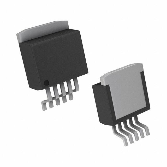
Figure 4. 5-Lead TO-263 Surface Mount Package
Package Number KTT0005B
These devices have limited built-in ESD protection. The leads should be shorted together or the device placed in conductive foam
during storage or handling to prevent electrostatic damage to the MOS gates.
Absolute Maximum Ratings
(1)
−26V to +40V
DC Input Voltage
Positive Input Transient (t 100 mA)
where the input voltage is applied through a long length of wire, which in effect adds a significant amount of
inductance in series with the input. The drop in input current may create a positive input voltage transient which
may take the PNP out of saturation. If the input voltage is held constant at the threshold where the PNP is going
in and out of saturation, an oscillation may be created.
This is only observed where a large series inductance is present in the input supply line and when the rise and
fall time of the input supply is very slow. If the application and removal of the input voltage changes at a rate
greater than 500 mV/μs it will move through the dropout region of the regulator (VIN of 3V to 5.5V) too quickly for
an oscillation to be established.
THERMAL MANAGEMENT
The LM9071 is packaged in both a TO-263 surface mount power package and a narrow lead-pitch TO-220
package. To obtain operation over the highest possible load current and input voltage ranges, care must be
taken to control the operating temperature of the device. Thermal shutdown protection is built in, with a threshold
above 150°C. Conventional heat-sinking techniques can be used with the TO-220 package. When applying the
TO-263 package, on board heat-sinking is important to prevent premature thermal shutdown. More copper foil
area under the tab of the device will directly improve the operating θJ-A of the TO-263 package, which will reduce
the junction temperature of the device.
The θJ-A value for the TO-263 package (still air, no additional heat sink) is rated at 80°C/W. The effective θJ-A
value of the TO-263 package can be reduced by increasing the printed circuit board area that is connected
(soldered) to the package tab. Using 1 ounce (1.4 mils thick) copper clad with no solder mask, an area of 0.5
square inches will reduce θJ-A to 50°C/W, an area of 1.0 square inches will reduce θJ-Ato 37°C/W, and an area of
1.6 square inches will reduce θJ-A to 32°C/W. If the printed circuit board uses a solder mask, the copper clad area
under the solder mask should be increased by at least 50% to maintain a similar θJ-A rating.
The use of a double sided PC board with soldered filled vias between two planes of copper, as shown in
Figure 16, will improve thermal performance while optimizing the PC board surface area required. Using the
double sided PC board arrangement shown in Figure 16, with 1 ounce (1.4 mils thick) copper clad with no solder
mask and solder filled vias, an area of 0.5 square inches on both sides will reduce θJ-A to 43°C/W.
Submit Documentation Feedback
Copyright © 1999–2013, Texas Instruments Incorporated
Product Folder Links: LM9071
7
�LM9071
SNVS131D – DECEMBER 1999 – REVISED APRIL 2013
www.ti.com
Figure 16. Typical TO-263 PC Board Heatsinking
8
Submit Documentation Feedback
Copyright © 1999–2013, Texas Instruments Incorporated
Product Folder Links: LM9071
�LM9071
www.ti.com
SNVS131D – DECEMBER 1999 – REVISED APRIL 2013
REVISION HISTORY
Changes from Revision C (April 2013) to Revision D
•
Page
Changed layout of National Data Sheet to TI format ............................................................................................................ 8
Submit Documentation Feedback
Copyright © 1999–2013, Texas Instruments Incorporated
Product Folder Links: LM9071
9
�PACKAGE OPTION ADDENDUM
www.ti.com
10-Dec-2020
PACKAGING INFORMATION
Orderable Device
Status
(1)
Package Type Package Pins Package
Drawing
Qty
Eco Plan
(2)
Lead finish/
Ball material
MSL Peak Temp
Op Temp (°C)
Device Marking
(3)
(4/5)
(6)
LM9071S/NOPB
ACTIVE
DDPAK/
TO-263
KTT
5
45
RoHS-Exempt
& Green
SN
Level-3-245C-168 HR
-40 to 125
LM9071S
LM9071SX/NOPB
ACTIVE
DDPAK/
TO-263
KTT
5
500
RoHS-Exempt
& Green
SN
Level-3-245C-168 HR
-40 to 125
LM9071S
(1)
The marketing status values are defined as follows:
ACTIVE: Product device recommended for new designs.
LIFEBUY: TI has announced that the device will be discontinued, and a lifetime-buy period is in effect.
NRND: Not recommended for new designs. Device is in production to support existing customers, but TI does not recommend using this part in a new design.
PREVIEW: Device has been announced but is not in production. Samples may or may not be available.
OBSOLETE: TI has discontinued the production of the device.
(2)
RoHS: TI defines "RoHS" to mean semiconductor products that are compliant with the current EU RoHS requirements for all 10 RoHS substances, including the requirement that RoHS substance
do not exceed 0.1% by weight in homogeneous materials. Where designed to be soldered at high temperatures, "RoHS" products are suitable for use in specified lead-free processes. TI may
reference these types of products as "Pb-Free".
RoHS Exempt: TI defines "RoHS Exempt" to mean products that contain lead but are compliant with EU RoHS pursuant to a specific EU RoHS exemption.
Green: TI defines "Green" to mean the content of Chlorine (Cl) and Bromine (Br) based flame retardants meet JS709B low halogen requirements of
很抱歉,暂时无法提供与“LM9071S/NOPB”相匹配的价格&库存,您可以联系我们找货
免费人工找货