OBSOLETE
LM9072
www.ti.com
SNVS134D – DECEMBER 1999 – REVISED APRIL 2013
LM9072 Dual Tracking Low-Dropout System Regulator
Check for Samples: LM9072
FEATURES
DESCRIPTION
•
The LM9072 is a high performance voltage regulator
system with operational and protection features that
address
many
requirements
of
automotive
applications. Two regulated outputs are provided. The
main regulator provides a precision 2% maximum
tolerance 5V output at 350mA with a low dropout
characteristic. The second regulator provides a 5V
output that tracks the main regulator output voltage
within 1.5% with load currents up to 80mA. The
tracking output is ideal for use in powering remotely
located sensors with outputs that are ratiometric to
the main system supply. This output is fully protected
from short circuits to ground or the unregulated input
supply (ignition or battery potentials in automotive
applications).
1
2
•
•
•
•
•
•
•
•
•
Two 5V Regulated Outputs:
– 350 mA, 2% Main Output
– 80 mA, 1.5% Tracking Output
Good EMI (1 MHz to 400 MHz, BCI) Immunity
Separate ON/OFF and Keep-Alive Control
Inputs
Less Than 100 μA Quiescent Current in OFF
State
Programmable Delayed Reset Output
Input Transient Protection Over 60V to −45V
Tracking Output Protected From Shorts to
Battery
Less Than 1V Dropout at Full Load
−40°C to +125°C Operating Temperature Range
Surface Mount SFM Power Package
TYPICAL APPLICATIONS
•
•
•
•
•
Automotive Module Supply Power
Conditioning
Remote Sensor Biasing
Ratiometric to Supply Sensor Detection
Continuous Operation for Save Routines and
EPROM Programming After Power Down
Command
Safety Related Systems—EMC Operational
The LM9072 also contains a programmable delayed
system reset output. Two control inputs are provided.
An ON/OFF input intended for connection to an
ignition switch, and a Keep Alive input to allow a
system to remain powered after ignition has been
switched OFF.
For EMC concerns the LM9072 remains fully
operational and does not generate false rest signals
while subjected to, 1MHz to 400 MHz bulk current
injection signals greater than 100 mA on the input
supply and tracking output lines.
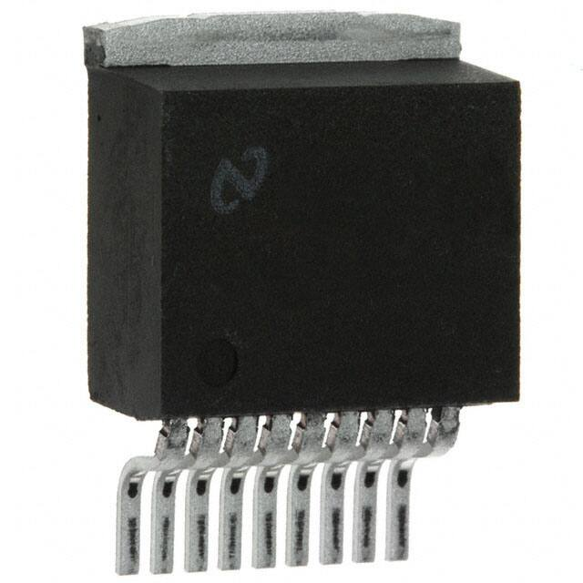
CONNECTION DIAGRAM
Backside metal is internally connected to ground.
9-Lead SFM
Surface Mount Power Package
Figure 1. See Package Number KTW
9-Lead TO-220 Package
Figure 2. See Package Number TA9A
1
2
Please be aware that an important notice concerning availability, standard warranty, and use in critical applications of
Texas Instruments semiconductor products and disclaimers thereto appears at the end of this data sheet.
All trademarks are the property of their respective owners.
PRODUCTION DATA information is current as of publication date.
Products conform to specifications per the terms of the Texas
Instruments standard warranty. Production processing does not
necessarily include testing of all parameters.
Copyright © 1999–2013, Texas Instruments Incorporated
�OBSOLETE
LM9072
SNVS134D – DECEMBER 1999 – REVISED APRIL 2013
www.ti.com
These devices have limited built-in ESD protection. The leads should be shorted together or the device placed in conductive foam
during storage or handling to prevent electrostatic damage to the MOS gates.
ABSOLUTE MAXIMUM RATINGS (1) (2)
−45V to 45V
Input Voltage (Continuous)
Input Voltage (Transient, t ≤ 400 ms)
Forced Output Voltages
60V
−0.3V to 7V
Main Output
−0.3V to 27V
Tracking Output
ON/OFF Input Voltage
(3)
−0.3V to 16V
ON/OFF Input Current
± 20 mA
−0.3V to 7V
Keep Alive In, Reset Out, CDELAY Voltage
Junction Temperature
150°C
−65°C to +150°C
Storage Temperature Range
ESD Susceptibility
(4)
2000V
Lead Temperature (Soldering, 10 seconds)
(1)
(2)
(3)
(4)
265°C
Absolute Maximum Ratings indicate limits beyond which damage to the device may occur. Operating Ratings indicate conditions for
which the device remains functional but do not ensure specific performance limits. For ensured specifications and test conditions see the
Electrical Characteristics.
If Military/Aerospace specified devices are required, please contact the Texas Instruments Sales Office/Distributors for availability and
specifications.
The ON/OFF input is internally clamped to a 7V zener diode through a 1 kΩ resistor.
Human body model, 150 pF capacitor discharged through a 1.5 kΩ resistor.
OPERATING RATINGS (1)
Input Voltage Range
6V to 27V
−40°C to +125°C
Ambient Temperature Range
TO-220 Thermal Resistance, θJ-C
3°C/W
TO-220 Thermal Resistance, θJ-A (2)
73°C/W
SFM Thermal Resistance, θJ-C
3°C/W
SFM Thermal Resistance, θJ-A (3)
(1)
(2)
(3)
80°C/W
Absolute Maximum Ratings indicate limits beyond which damage to the device may occur. Operating Ratings indicate conditions for
which the device remains functional but do not ensure specific performance limits. For ensured specifications and test conditions see the
Electrical Characteristics.
Exceeding the Maximum Allowable power dissipation will cause excessive die temperature, and the device will go into thermal
shutdown. The θJ-A value for the TO-220 package (still air, no additional heat sink) is 73°C/W. The effective θJ-A value of the TO-220
package can be reduced by using conventional heat sink methods.
Exceeding the Maximum Allowable power dissipation will cause excessive die temperature, and the device will go into thermal
shutdown. The θJ-A value for the SFM package (still air, no additional heat sink) is 80°C/W. The effective θJ-A value of the SFM package
can be reduced by increasing the printed circuit board area that is connected (soldered) to the package tab. Using 1 ounce (1.4 mils
thick) copper clad with no solder mask, an area of 0.5 square inches will reduced θJ-A to 50°C/W, an area of 1.0 square inches will
reduced θJ-Ato 37°C/W, ad an area of 1.6 square inches will reduced θJ-A to 32°C/W. If the printed circuit board uses a solder mask, the
copper clad area should be increased by at least 50% to maintain a similar θJ-A rating.
ELECTRICAL CHARACTERISTICS (1)
6.0V ≤ VIN ≤ 19V, TCASE = 25°C, unless otherwise specified. COUT ≥ 6 μF with 0.3Ω ≤ ESR ≤ 3Ω on each regulator output.
Symbol
Parameter
Conditions
Min
Max
Units
5 mA ≤ ILOAD ≤ 350 mA
−40°C ≤ TCASE ≤ 125°C
4.9
5.1
V
19V ≤ VIN ≤ 30V
5 mA ≤ ILOAD ≤ 350 mA
−40°C ≤ TCASE ≤ 125°C
4.8
5.2
V
MAIN REGULATOR
VMAIN
Main Output Voltage
RMLOAD
Load Regulation
VIN = 16V, 5 mA ≤ ILOAD ≤ 350 mA
25
mV
RMLINE
Line Regulation
ILOAD = 350 mA, 8V ≤ VIN ≤ 16V
25
mV
(1)
2
Datasheet min/max specifications are specified by design, test, and/or statistical analysis.
Submit Documentation Feedback
Copyright © 1999–2013, Texas Instruments Incorporated
Product Folder Links: LM9072
�OBSOLETE
LM9072
www.ti.com
SNVS134D – DECEMBER 1999 – REVISED APRIL 2013
ELECTRICAL CHARACTERISTICS(1) (continued)
6.0V ≤ VIN ≤ 19V, TCASE = 25°C, unless otherwise specified. COUT ≥ 6 μF with 0.3Ω ≤ ESR ≤ 3Ω on each regulator output.
Symbol
Parameter
VMDO
Dropout Voltage, VIN–VMAIN
VSD
Overvoltage Shutdown Threshold
IMSC
Output Short Circuit Current
RMRR
Ripple Rejection
Conditions
Min
VIN > 5.5V, 5 mA ≤ ILOAD ≤ 350 mA
(2)
Max
Units
0.8
V
30
36
V
RL = 1Ω
450
1000
mA
VIN = 9V, 50 ≤ Freq ≤ 20 kHz,
VRIPPLE = 4VP-P
40
dB
TRACKING REGULATOR
VTRACK
VERROR
Tracking Output Voltage
Output Tracking Error
(VMAIN–VTRACK)
1 mA ≤ ILOAD ≤ 80 mA
−40°C ≤ TCASE ≤ 125°C
4.85
5.15
V
19V ≤ VIN ≤ 30V
1 mA ≤ ILOAD ≤ 80 mA
−40°C ≤ TCASE ≤ 125°C
4.725
5.275
V
−50
50
mV
0.8
V
200
mA
27
V
1 mA ≤ ILOAD ≤ 80 mA
(2)
VTDO
Dropout Voltage,
VIN–VTRACK
VIN > 5.5V, 1 mA ≤ ILOAD ≤ 80 mA
ITSC
Output Short Circuit Current
RL = 1Ω
VTSC
Output Short Circuit Voltage
No Effect On Other Functions
−2
RTRR
Ripple Rejection
VIN = 9V, 50 ≤ Freq ≤ 20 kHz,
VRIPPLE = 4VP-P
40
dB
INPUT CURRENT
Quiescent Input Current with
Both Regulators OFF
8V ≤ VIN ≤ 16V
40
μA
16V ≤ VIN ≤ 42V
10
mA
Iq
No Load Quiescent Current
8V ≤ VIN ≤ 19V, IL = 0 mA
15
mA
InON
Additional Input Current with
Both Regulators ON
VIN > 8V, ILtotal = ILmain + ILtrack
ILtotal = 350 mA + 80 mA = 430 mA
1.2
x ILtotal
Iindo
Additional Input Current in Dropout
0V < VIN < 8V, (3)
ILtotal = ILmain + ILtrack
ILtotal = 350 mA + 80 mA = 430 mA
1.5
x ILtotal
IqOFF
RESET OUTPUT
VTHRL
Low Switching Threshold
VMAIN Output Controls Reset
4.45
4.75
V
VTHRH
High Switching Threshold
VMAIN Output Controls Reset
5.40
5.75
V
VLOW
Logic Low Output Voltage
1V ≤ VMAIN ≤ VTHRL,
RRESET = 50 kΩ to VMAIN
0.4
V
VHIGH
Logic High Output Voltage
Normal Operation,
VTHRL ≤ VMAIN ≤ VTHRH, ISOURCE = 0
VMAIN–
50 mV
VMAIN
V
RP-U
Internal Output Pull-Up Resistance
2.4
6.0
kΩ
TDELAY
Reset Delay Interval
35
70
ms
CDELAY = 0.1 μF (Low Leakage),
IDELAY for Charging the Delay Capacitor is
Typically 6 μA
TRISE
Output Rise Time
From 10% VMAIN to 90% VMAIN
CLRESET = 50 pF
1.5
μs
TFALL
Output Fall Time
From 90% VMAIN to 10% VMAIN
CLRESET = 50 pF
0.5
μs
3.5
4.5
V
1.5
2.5
V
CONTROL INPUTS
VON
ON Threshold for ON/OFF Input
RSERIES = 22 kΩ
VOFF
OFF Threshold for ON/OFF Input
RSERIES = 22 kΩ
(2)
(3)
(4)
(4)
The dropout voltage specifications actually indicate the saturation voltage of the PNP power transistors used in each regulator. Over the
full load current and temperature ranges both regulators will output at least 4.7V with an input voltage of only 5.5V.
The input quiescent current will increase when the regulators are in dropout conditions. The amount of additional input currents is a
direct function of the total load current on both outputs. The peak increase in current is limited to 50% of the total load current.
If either control input is left open circuited the regulators will turn OFF.
Submit Documentation Feedback
Copyright © 1999–2013, Texas Instruments Incorporated
Product Folder Links: LM9072
3
�OBSOLETE
LM9072
SNVS134D – DECEMBER 1999 – REVISED APRIL 2013
www.ti.com
ELECTRICAL CHARACTERISTICS(1) (continued)
6.0V ≤ VIN ≤ 19V, TCASE = 25°C, unless otherwise specified. COUT ≥ 6 μF with 0.3Ω ≤ ESR ≤ 3Ω on each regulator output.
Symbol
Parameter
Conditions
ION/OFF
ON/OFF Input Current
1.4V ≤ VON/OFF ≤ 4.5V
−0.3V ≤ VON/OFF ≤ 7V
ONK-A
Turn ON Threshold for Keep Alive Input
OFFK-A
Turn OFF Threshold for Keep Alive Input
RP-D
Pull-Down Resistance at Keep Alive Input 0V ≤ VK-A ≤ 5V
(5)
4
(5)
Min
Max
1
12
μA
−1
5
mA
2
(4)
5
Units
V
0.8
V
40
kΩ
The ON/OFF input is internally clamped to a 7V zener diode through a 1 kΩ resistor.
Submit Documentation Feedback
Copyright © 1999–2013, Texas Instruments Incorporated
Product Folder Links: LM9072
�OBSOLETE
LM9072
www.ti.com
SNVS134D – DECEMBER 1999 – REVISED APRIL 2013
TYPICAL PERFORMANCE CHARACTERISTICS
(TA = 25°C unless otherwise specified)
Turn-ON Characteristic
Turn-OFF Characteristic
Figure 3.
Figure 4.
Normalized Main Output Voltage vs Temperature
Quiescent Input Current vs Input Voltage
Figure 5.
Figure 6.
Main Output Voltage at Input Voltage Extremes
Input Current vs Input Voltage (Regulators OFF)
Figure 7.
Figure 8.
Submit Documentation Feedback
Copyright © 1999–2013, Texas Instruments Incorporated
Product Folder Links: LM9072
5
�OBSOLETE
LM9072
SNVS134D – DECEMBER 1999 – REVISED APRIL 2013
www.ti.com
TYPICAL PERFORMANCE CHARACTERISTICS (continued)
(TA = 25°C unless otherwise specified)
6
Tracking Output Short
Circuit Current
Main Regulator Dropout Voltage vs Load Current
Figure 9.
Figure 10.
Output Short Circuit Current vs Temperature
Reverse Battery Input Current
Figure 11.
Figure 12.
Maximum Power Dissipation
Output Capacitor ESR
Figure 13.
Figure 14.
Submit Documentation Feedback
Copyright © 1999–2013, Texas Instruments Incorporated
Product Folder Links: LM9072
�OBSOLETE
LM9072
www.ti.com
SNVS134D – DECEMBER 1999 – REVISED APRIL 2013
OPERATIONAL CHARACTERISTICS
Table 1. Control Logic Truth Table
ON/OFF
Input
Keep-Alive
Input
Main
Output
Voltage
Tracking
Output
Voltage
Reset
Output
L
L
0V
0V
0V
Operating Condition
OFF, Input Current < 100 μA
↑
L
5V
5V
↑ After Delay
H
X
5V
5V
5V
Normal ON Condition
H
X
< 4.45V
< 4.45V
0V
Main Output Pulled Out of Regulation, Reset Flag Generated
↓
H
5V
5V
5V
Keep-Alive, Continued Normal Operation
L
↑
5V
5V
↑ After Delay
Outputs Turned ON by Keep-Alive Input
Outputs Turn ON, Power ON Delayed Reset
Submit Documentation Feedback
Copyright © 1999–2013, Texas Instruments Incorporated
Product Folder Links: LM9072
7
�OBSOLETE
LM9072
SNVS134D – DECEMBER 1999 – REVISED APRIL 2013
www.ti.com
APPLICATION INFORMATION
PIN DESCRIPTION AND FUNCTIONALITY
The LM9072 is a precision dual tracking voltage regulator optimized for use in powertrain module applications
but will also find use in a wide variety of automotive and industrial applications where precision supply regulation
is required in harsh operating environments. The following will describe the functionality of each of the package
pins.
INPUT VOLTAGE (Pin 3)
The LM9072 has been designed to connect directly to the ignition or battery supply in automotive applications.
For this type of supply the regulator has been designed to withstand up to +60V and −45V supply transients such
as load dump. An overvoltage shut down protection scheme turns OFF both of the regulator outputs should
supply transients exceed typically +33V to fully protect all load circuitry. This higher threshold allows normal
operation with 24 VDC applied to the input as in the event when two batteries are used to start a vehicle.
Protection of the system is also provided for inadvertent reverse polarity battery connections.
The current drain on the supply line is directly proportional to the load currents on the two voltage regulators.
With no load current on either output the regulator requires 15 mA maximum quiescent current for biasing
internal circuitry. During dropout conditions (VIN < 5.5V) the additional input current can rise to 50% of the total
load current. With less than 4V applied to the input, internal biasing circuitry shuts OFF.
When switched OFF the regulator can remain connected to the battery supply with a current drain of less than
100 μA.
Figure 15. Circuit Block Diagram
MAIN OUTPUT (Pin 9)
The Main Output regulator provides a well controlled (3% tolerance maximum) 5V supply line with a total load
current ranging up to 350 mA. This relatively high level of output current is sufficient to provide power to a large
number of load circuits in a variety of module applications.
This output has a short to ground current limit between 500 mA and 1A. The Main output can also withstand a
short circuit to potentials up to 7V.
8
Submit Documentation Feedback
Copyright © 1999–2013, Texas Instruments Incorporated
Product Folder Links: LM9072
�OBSOLETE
LM9072
www.ti.com
SNVS134D – DECEMBER 1999 – REVISED APRIL 2013
To maintain stability of this supply line an output bypass capacitor is required. This capacitor must be at least
6 μF with an equivalent series resistance (ESR) between 0.3Ω and 3Ω over temperature.
The Main Output is sensed for the generation of the system reset output. Feedback from the Main Output is also
used to control the output voltage of the tracking regulator.
TRACKING OUTPUT (Pin 4)
The Tracking Output regulator is a key feature of the LM9072. This output provides a voltage that directly tracks
the main output voltage within 1.5%. This 80 mA output is provided to bias sensors and other devices located
external to the main system module.
For providing remote power the Tracking Output is fully protected against short circuit connections to the battery
or input supply (up to 27V) and to ground. These shorted fault conditions do not affect the operation of the main
supply nor generate a reset of the system.
The tracking characteristic allows for ratiometric operation of sensors by providing power that is directly
proportional to the system supply. Similar to the main output a bypass capacitor is required for stability. This
capacitor should also be greater than 6 μF with an ESR between 0.3Ω and 3Ω.
RESET OUTPUT (Pin 6)
The Reset Output is an active low logic signal provided to reset a system microcontroller on power up and in the
event that the Main Output supply falls out of regulation. This output is ensured to provide a logic low level (<
0.4V) whenever the Main Output supply is below 4.45V or is pulled above 5.75V. This general reset prevents
erratic system operation which may occur with out-of-specification supply potentials.
The Reset Output has an active pull down to ground and a passive pull-up (through a 4 kΩ resistor) to the Main
Output to ensure voltage compatibility with the system supply. Capacitive loading on this reset line will directly
affect the rise time of the reset signal. The Reset Output will maintain a logic low level with a Main Output voltage
of only 1V. Below 1V the active pull-down device switches OFF (sink current of only 500 μA), but with such a low
supply potential, system controllers are generally inoperative.
The Reset Output has a built-in delay time interval which is programmable by the selection of the delay
capacitor.
DELAY CAPACITOR (Pin 7)
The Delay Capacitor (CDELAY) controls a time interval that the Reset Output remains low after the Main Output
has established normal operating condition. This feature holds the system in reset for a time to allow all load
circuitry to be properly biased before executing functions. This interval is applied at power-up and following any
event that may trigger the system reset function.
Figure 16 illustrates the delayed reset generator. Two comparators continually monitor the Main Output supply.
Window comparators C1 and C2 detect if the Main Supply is below 4.6V or exceeds 5.5V typically. If this is true
(at power-on, for example) the control logic turns ON the discharge transistor and holds CDELAY low (at 0.9V).
Comparator C4 then outputs a logic low system Reset signal within 2 μs after detecting the out of regulation
condition.
The Delay Capacitor remains discharged until the window comparator senses that the Main Output is within
normal operating range (C1 and C2 outputs are both low). When this condition is met, the discharge transistor is
turned OFF and CDELAY is charged positively by an internal 6 μA current source. The Reset Output will remain
low un the delay capacitor has reached 4V, at which point it will go high and the system will begin normal
operation. This delay time interval is controlled by the selection of CDELAY and can be determined from the
following equation:
TDELAY = (0.5 x 10⁶) • CDELAY
(1)
Typically a 0.1 μF capacitor will produce a delay interval of 50 ms.
To ensure a consistent delay time interval, the discharge transistor is always latched ON by the window
comparators, and can not be switched OFF to start a new delay interval until CDELAY has been discharged to less
than or equal to 0.9V. This sets a fixed starting voltage (0.9V) and ending voltage (4V) for the charging of the
Delay Capacitor.
Submit Documentation Feedback
Copyright © 1999–2013, Texas Instruments Incorporated
Product Folder Links: LM9072
9
�OBSOLETE
LM9072
SNVS134D – DECEMBER 1999 – REVISED APRIL 2013
www.ti.com
ON/OFF INPUT (Pin 1)
The ON/OFF Input enables both the Main and Tracking outputs. In a typical application this input is connected to
the input supply through a series resistor (nominally 22 kΩ) and a switch (Ignition, as an example). When the
switch is closed this input is pulled high and switches ON both regulator outputs. This input is internally clamped
to a 7V zener diode through a series 1 kΩ resistor. The external series resistor together with an optional 0.1 μF
capacitor to ground are optional to provide filtering and current limiting to withstand any transients that may
appear on the input supply in order to maintain normal operation of the system.
The switching threshold of the ON/OFF comparator has 2V of hysteresis to ensure noise free control of the
system. To turn the regulators ON this input must be taken above 4V. To turn the system OFF the ON/OFF Input
must be open circuited or taken below 2V.
Figure 16. Reset Generator
KEEP-ALIVE INPUT (Pin 8)
This CMOS logic level compatible input provides a system with the ability to control its own ON/OFF sequencing.
The Keep-Alive Input is OR'ed with the ON/OFF Input so either one can independently control the regulators.
As shown in the Operational Characteristics a system controller can take the Keep-Alive input high at any time. If
the ON/OFF switch is opened, this high level on Keep-Alive will keep the regulators ON and the entire system
operational. This control is useful for providing as much time as necessary for a system to perform
“housekeeping” chores such as programming EEPROM with system information prior to turning itself OFF (by
taking the Keep-Alive Input low) and reverting to the low quiescent current state.
A second use of the Keep-Alive Input can be from other modules which need information from the module
powered by the LM9072, Figure 17. A CMOS logic high level (> 2V) on this input will power up the system as
needed independent from the normal ON/OFF switch.
10
Submit Documentation Feedback
Copyright © 1999–2013, Texas Instruments Incorporated
Product Folder Links: LM9072
�OBSOLETE
LM9072
www.ti.com
SNVS134D – DECEMBER 1999 – REVISED APRIL 2013
Figure 17. Remote ON/OFF Control
SYSTEM KEEP-ALIVE OPERATION
Figure 18 illustrates the basic concept of Keep-Alive operation. The LM9072 provides regulated supplies to an
entire microcontroller based system or module including remote sensors. The system is switched ON or OFF by
a switch connected to the unregulated input supply and the ON/OFF input, pin 1. When closed the regulators
turn ON and the system is held in a reset state for the duration of the delayed reset interval controlled by CDELAY.
Once normal operation of the system begins, the controller needs to set an output line connected to the KeepAlive input, pin 8, high. The system remains in normal operation until switched OFF by opening the ON/OFF
switch. With Keep-Alive high the entire system remains normally biased and will remain operational until the
Keep-Alive input is taken low.
Transistor Q1 is shown as a means to inform the controller that the ON/OFF switch has been opened. This high
level on an input line tells the controller that the system has been switched OFF. This indicates the start of the
Keep-Alive interval. The system can perform whatever actions required to obtain the proper OFF state before
actually powering down. These general housekeeping tasks can include putting external devices in the proper
OFF condition and storing various system variables in EPROM for example. With the controller in command of
the Keep-Alive interval these tasks can take whatever time necessary to complete.
When completed the controller takes the Keep-Alive input to a low level and the entire system shuts down. The
LM9072 powers down to a low quiescent current mode with less than 100 μA drawn from the input supply.
To initiate the Keep-Alive routine before actual power down, it is important for the system controller to know
when the system has been switched OFF. To eliminate any interface between the controller and the ON/OFF
switch and potentially noisy unregulated input supply, a simple logic scheme shown in Figure 19 can be used.
With this circuitry the Reset output from the LM9072 provides the ON/OFF sensing input to the controller.
When switched OFF, the main regulator output will fall out of regulation and generate a low logic level on the
Reset output. This input to the controller provides the switch OFF indication and initiates the Keep-Alive interval.
Control of the Keep-Alive duration is set by a logic 1 on the Keep-Alive output line from the system controller.
This high level prevents the Reset output from resetting the entire system and also gates the Keep-Alive input
signal to the LM9072. The inverted Reset signal provides a logic 1 to the Keep-Alive input of the LM9072.
The Main output will only drop out of regulation for a very short time before the Keep-Alive input turns it back on.
The Reset output remains low for the delay time interval. When it returns high the Main output switches OFF and
back ON again very quickly. This continues until the system controller takes the Keep-Alive output line to a logic
low level.
Submit Documentation Feedback
Copyright © 1999–2013, Texas Instruments Incorporated
Product Folder Links: LM9072
11
�OBSOLETE
LM9072
SNVS134D – DECEMBER 1999 – REVISED APRIL 2013
www.ti.com
Figure 18. Basic Keep-Alive Operation
12
Submit Documentation Feedback
Copyright © 1999–2013, Texas Instruments Incorporated
Product Folder Links: LM9072
�OBSOLETE
LM9072
www.ti.com
SNVS134D – DECEMBER 1999 – REVISED APRIL 2013
Figure 19. Simple Logic Configuration to Provide ON/OFF Sensing
SAFETY LATCH-OFF
To address a system FMEA (Failure Mode Effects Analysis) issue the Keep-Alive high level should be derived
from the Tracking output regulator as shown in Figure 20. The issue stems from the “what-if” scenario whereby
the system is in the Keep-Alive state and there is a short to ground on the Tracking Output regulator. If this
output is powering remote sensors or systems, this becomes a more highly possible fault condition. Since a short
on the Tracking output does not affect the Main output, which, if used to provide the Keep-Alive input signal,
would remain ON and draw 120 mA, the short circuit current of the Tracking regulator, from the input supply.
Using the Tracking output supply for Keep-Alive would prevent Keep-Alive operation during a short to ground
fault and the excessive drain on the input supply. The inversion by the transistor will require a low level from the
controller to allow Keep-Alive operation. The 24 kΩ pull-up resistor provides current limiting in the event of a
Tracking output short to the unregulated/battery input supply.
Submit Documentation Feedback
Copyright © 1999–2013, Texas Instruments Incorporated
Product Folder Links: LM9072
13
�OBSOLETE
LM9072
SNVS134D – DECEMBER 1999 – REVISED APRIL 2013
www.ti.com
Figure 20. Safety Latch-OFF
INPUT STABILITY
Low dropout voltage regulators which utilize a PNP power transistor usually exhibit a large increase in current
when in dropout (VIN < 5.5V). This increase is caused by the saturation characteristics (β reduction) of the PNP
transistor. To significantly minimize this increase in current the LM9072 detects when the PNP enters saturation
and reduces the operating current.
This reduction in input current can create a stability problem in applications with higher load current (> 200 mA)
where the input voltage is applied through a long length of wire which in effect add a significant amount of
inductance in series with the input. The drop in input current may create a positive input voltage transient which
may take the PNP out of saturation. If the input voltage is held constant at the threshold where the PNP is going
in and out of saturation, an oscillation may be created.
This is only observed where a large series inductance is present in the input supply line and when the rise and
fall time of the input supply is very slow. If the application and removal of the input voltage changes at a rate
greater than 500 mV/ms it will move through the dropout region of the regulator (VIN of 3V to 5.5V) too quickly for
an oscillation to be established.
In the event that an oscillation is present, input bypassing can also help de-tune the resonance. Figure 21
illustrates two input bypassing approaches. The straightforward addition of a larger valued electrolytic capacitor
could suffice. in this case however, if reverse battery connections are a possibility it is necessary to add a series
protection diode as shown to prevent damaging the polarized input capacitor.
An alternative input bypassing scheme is also shown. This eliminates the use of polarized input capacitors and a
series protection diode. The values shown were derived empirically in a representative typical application.
Appropriate values for any given application require experimentation.
14
Submit Documentation Feedback
Copyright © 1999–2013, Texas Instruments Incorporated
Product Folder Links: LM9072
�OBSOLETE
LM9072
www.ti.com
SNVS134D – DECEMBER 1999 – REVISED APRIL 2013
Figure 21. Input Bypassing
THERMAL MANAGEMENT
The LM9072 is packaged in both a SFM surface mount power package and a narrow lead-pitch TO-220
package. To obtain operation over the highest possible load current and input voltage ranges, care must be
taken to control the operating temperature of the device. Thermal shutdown protection is built in, with a threshold
above 150°C. Conventional heat-sinking techniques can be used with the TO-220 package. When applying the
SFM package, on board heat-sinking is important to prevent premature thermal shutdown. More copper foil area
under the tab of the device will directly improve the operating θJ-A of the SFM package, which will reduce the
junction temperature of the device.
The θJ-A value for the SFM package (still air, no additional heat sink) is rated at 80°C/W. The effective θJ-A value
of the SFM package can be reduced by increasing the printed circuit board area that is connected (soldered) to
the package tab. Using 1 ounce (1.4 mils thick) copper clad with no solder mask, an area of 0.5 square inches
will reduce θJ-A to 50°C/W, an area of 1.0 square inches will reduce θJ-Ato 37°C/W, and an area of 1.6 square
inches will reduce θJ-A to 32°C/W. If the printed circuit board uses a solder mask, the copper clad area under the
solder mask should be increased by at least 50% to maintain a similar θJ-A rating.
The use of a double sided PC board with soldered filled vias between two planes of copper, as shown in
Figure 22, will improve thermal performance while optimizing the PC board surface area required. Using the
double sided PC board arrangement shown in Figure 22, with 1 ounce (1.4 mils thick) copper clad with no solder
mask and solder filled vias, an area of 0.5 square inches on both sides will reduce θJ-A to 43°C/W.
Submit Documentation Feedback
Copyright © 1999–2013, Texas Instruments Incorporated
Product Folder Links: LM9072
15
�OBSOLETE
LM9072
SNVS134D – DECEMBER 1999 – REVISED APRIL 2013
www.ti.com
Figure 22. Typical SFM PC Board Heatsinking
ELECTRO-MAGNETIC COMPATIBILITY (EMC)
The LM9072 offers good immunity to high frequency interference in a standard Bulk Current Injection (BCI) test
(ISO11452 Part 4 test method). The following test conditions and configuration (Figure 23) can be used to
observe this performance.
Frequency Range
1 MHz to 400 MHz
Modulation 1
CW (no modulation)
Modulation 2
1 kHz sine wave, 80% AM
Dwell Time
1 second
Frequency Steps
1 MHz (from 1 MHz to 10 MHz)
2 MHz (from 10 MHz to 200 MHz)
20 MHz (from 200 MHz to 400 MHz)
Test Method
Closed loop current probe
In this test configuration the current injected into either the input pin or the tracking output pin is increased until a
reset output is generated. These two pins are the most critical as they typically will connect to a module through
long lengths of wire most likely to pick up high frequency energy. Figure 24 illustrates examples of test results on
the LM9072 with both types of modulation.
These results are just examples as actual results in any given application will depend on numerous external
factors such as component selection, pc board layout, etc. The current power of the injected signal is expressed
in dB relative to 1 mA (i.e., 40 dBmA = 100 mA).
16
Submit Documentation Feedback
Copyright © 1999–2013, Texas Instruments Incorporated
Product Folder Links: LM9072
�OBSOLETE
LM9072
www.ti.com
SNVS134D – DECEMBER 1999 – REVISED APRIL 2013
Figure 23. Bulk Current Injection Test Configuration
BCI Susceptibility, Modulation 1 (CW)
BCI Susceptibility Moduiatlon 2 (1 kHz, 80% AM
modulation)
Figure 24. Examples of BCI Test Results
Submit Documentation Feedback
Copyright © 1999–2013, Texas Instruments Incorporated
Product Folder Links: LM9072
17
�OBSOLETE
LM9072
SNVS134D – DECEMBER 1999 – REVISED APRIL 2013
www.ti.com
REVISION HISTORY
Changes from Revision C (April 2013) to Revision D
•
18
Page
Changed layout of National Data Sheet to TI format .......................................................................................................... 17
Submit Documentation Feedback
Copyright © 1999–2013, Texas Instruments Incorporated
Product Folder Links: LM9072
�IMPORTANT NOTICE
Texas Instruments Incorporated and its subsidiaries (TI) reserve the right to make corrections, enhancements, improvements and other
changes to its semiconductor products and services per JESD46, latest issue, and to discontinue any product or service per JESD48, latest
issue. Buyers should obtain the latest relevant information before placing orders and should verify that such information is current and
complete. All semiconductor products (also referred to herein as “components”) are sold subject to TI’s terms and conditions of sale
supplied at the time of order acknowledgment.
TI warrants performance of its components to the specifications applicable at the time of sale, in accordance with the warranty in TI’s terms
and conditions of sale of semiconductor products. Testing and other quality control techniques are used to the extent TI deems necessary
to support this warranty. Except where mandated by applicable law, testing of all parameters of each component is not necessarily
performed.
TI assumes no liability for applications assistance or the design of Buyers’ products. Buyers are responsible for their products and
applications using TI components. To minimize the risks associated with Buyers’ products and applications, Buyers should provide
adequate design and operating safeguards.
TI does not warrant or represent that any license, either express or implied, is granted under any patent right, copyright, mask work right, or
other intellectual property right relating to any combination, machine, or process in which TI components or services are used. Information
published by TI regarding third-party products or services does not constitute a license to use such products or services or a warranty or
endorsement thereof. Use of such information may require a license from a third party under the patents or other intellectual property of the
third party, or a license from TI under the patents or other intellectual property of TI.
Reproduction of significant portions of TI information in TI data books or data sheets is permissible only if reproduction is without alteration
and is accompanied by all associated warranties, conditions, limitations, and notices. TI is not responsible or liable for such altered
documentation. Information of third parties may be subject to additional restrictions.
Resale of TI components or services with statements different from or beyond the parameters stated by TI for that component or service
voids all express and any implied warranties for the associated TI component or service and is an unfair and deceptive business practice.
TI is not responsible or liable for any such statements.
Buyer acknowledges and agrees that it is solely responsible for compliance with all legal, regulatory and safety-related requirements
concerning its products, and any use of TI components in its applications, notwithstanding any applications-related information or support
that may be provided by TI. Buyer represents and agrees that it has all the necessary expertise to create and implement safeguards which
anticipate dangerous consequences of failures, monitor failures and their consequences, lessen the likelihood of failures that might cause
harm and take appropriate remedial actions. Buyer will fully indemnify TI and its representatives against any damages arising out of the use
of any TI components in safety-critical applications.
In some cases, TI components may be promoted specifically to facilitate safety-related applications. With such components, TI’s goal is to
help enable customers to design and create their own end-product solutions that meet applicable functional safety standards and
requirements. Nonetheless, such components are subject to these terms.
No TI components are authorized for use in FDA Class III (or similar life-critical medical equipment) unless authorized officers of the parties
have executed a special agreement specifically governing such use.
Only those TI components which TI has specifically designated as military grade or “enhanced plastic” are designed and intended for use in
military/aerospace applications or environments. Buyer acknowledges and agrees that any military or aerospace use of TI components
which have not been so designated is solely at the Buyer's risk, and that Buyer is solely responsible for compliance with all legal and
regulatory requirements in connection with such use.
TI has specifically designated certain components as meeting ISO/TS16949 requirements, mainly for automotive use. In any case of use of
non-designated products, TI will not be responsible for any failure to meet ISO/TS16949.
Products
Applications
Audio
www.ti.com/audio
Automotive and Transportation
www.ti.com/automotive
Amplifiers
amplifier.ti.com
Communications and Telecom
www.ti.com/communications
Data Converters
dataconverter.ti.com
Computers and Peripherals
www.ti.com/computers
DLP® Products
www.dlp.com
Consumer Electronics
www.ti.com/consumer-apps
DSP
dsp.ti.com
Energy and Lighting
www.ti.com/energy
Clocks and Timers
www.ti.com/clocks
Industrial
www.ti.com/industrial
Interface
interface.ti.com
Medical
www.ti.com/medical
Logic
logic.ti.com
Security
www.ti.com/security
Power Mgmt
power.ti.com
Space, Avionics and Defense
www.ti.com/space-avionics-defense
Microcontrollers
microcontroller.ti.com
Video and Imaging
www.ti.com/video
RFID
www.ti-rfid.com
OMAP Applications Processors
www.ti.com/omap
TI E2E Community
e2e.ti.com
Wireless Connectivity
www.ti.com/wirelessconnectivity
Mailing Address: Texas Instruments, Post Office Box 655303, Dallas, Texas 75265
Copyright © 2013, Texas Instruments Incorporated
�