LM94023
www.ti.com
SNIS150B – SEPTEMBER 2008 – REVISED JUNE 2013
1.5V, micro SMD, Dual-Gain Analog Temperature Sensor with Class AB Output
Check for Samples: LM94023
FEATURES
DESCRIPTION
•
•
The LM94023 is a precision analog output CMOS
integrated-circuit temperature sensor that operates at
a supply voltage as low as 1.5 Volts. Available in the
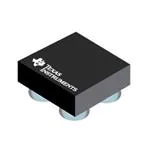
very small four-bump DSBGA 0.8mm x 0.8mm) the
LM94023 occupies very little board area. A class-AB
output structure gives the LM94023 strong output
source and sink current capability for driving heavy
loads, making it well suited to source the input of a
sample-and-hold analog-to-digital converter with its
transient load requirements, This generally means the
LM94023 can be used without external components,
like resistors and buffers, on the output. While
operating over the wide temperature range of −50°C
to +150°C, the LM94023 delivers an output voltage
that is inversely porportional to measured
temperature. The LM94023's low supply current
makes it ideal for battery-powered systems as well as
general temperature sensing applications.
1
2
•
•
•
•
•
•
Low 1.5V Operation
Push-pull Output with 50µA Source Current
Capability
Two Selectable Gains
Very Accurate Over Wide Temperature Range
of −50°C to +150°C
Low Quiescent Current
Output is Short-circuit Protected
Extremely Small DSBGA Package
Footprint Compatible with the Industrystandard LM20 Temperature Sensor
APPLICATIONS
•
•
•
•
•
•
•
Cell Phones
Wireless Transceivers
Battery Management
Automotive
Disk Drives
Games
Appliances
KEY SPECIFICATIONS
•
•
•
•
•
Supply Voltage 1.5V to 5.5V
Supply Current 5.4 μA (typ)
Output Drive ±50 μA
Temperature Accuracy
– 20°C to 40°C ±1.5°C
– –50°C to 70°C ±1.8°C
– –50°C to 90°C ±2.1°C
– –50°C to 150°C ±2.7°C
Operating Temperature −50°C to 150°C
A Gain Select (GS) pin sets the gain of the
temperature-to-voltage output transfer function. Either
of two slopes are selectable: −5.5 mV/°C (GS=0) or
−8.2 mV/°C (GS=1). In the lowest gain configuration,
the LM94023 can operate with a 1.5V supply while
measuring temperature over the full −50°C to +150°C
operating range. Tying GS high causes the transfer
function to have the largest gain for maximum
temperature sensitivity. The gain-select inputs can be
tied directly to VDD or Ground without any pull-up or
pull-down resistors, reducing component count and
board area. These inputs can also be driven by logic
signals allowing the system to optimize the gain
during operation or system diagnostics.
Connection Diagram
GND
(A2)
VDD
GS
(A1)
VOUT
(B2)
(B1)
Connections
(Top View)
Figure 1. DSBGA
Top View
See Package Number YFQ0004
1
2
Please be aware that an important notice concerning availability, standard warranty, and use in critical applications of
Texas Instruments semiconductor products and disclaimers thereto appears at the end of this data sheet.
All trademarks are the property of their respective owners.
PRODUCTION DATA information is current as of publication date.
Products conform to specifications per the terms of the Texas
Instruments standard warranty. Production processing does not
necessarily include testing of all parameters.
Copyright © 2008–2013, Texas Instruments Incorporated
�LM94023
SNIS150B – SEPTEMBER 2008 – REVISED JUNE 2013
www.ti.com
Typical Transfer Characteristic
Typical Application
Full-Range Celsius Temperature Sensor (−50°C to
+150°C) Operating from a Single Battery Cell
VDD (+1.5V to +5.5V)
VDD
Single
Battery Cell
LM94023
GS
VOUT
GND
Figure 2. Output Voltage vs Temperature
PIN DESCRIPTIONS
Label
GS
Pin Number
A1
Type
Equivalent Circuit
Logic Input
VDD
Function
Gain Select - Input for
selecting the slope of
the analog output
response
ESD
CLAMP
GND
GND
A2
Ground
VOUT
B1
Analog Output
VDD
B2
Power
Power Supply Ground
VDD
Outputs a voltage
which is inversely
proportional to
temperature
GND
Positive Supply Voltage
These devices have limited built-in ESD protection. The leads should be shorted together or the device placed in conductive foam
during storage or handling to prevent electrostatic damage to the MOS gates.
2
Submit Documentation Feedback
Copyright © 2008–2013, Texas Instruments Incorporated
Product Folder Links: LM94023
�LM94023
www.ti.com
SNIS150B – SEPTEMBER 2008 – REVISED JUNE 2013
Absolute Maximum Ratings (1)
−0.3V to +6.0V
Supply Voltage
−0.3V to (VDD + 0.3V)
Voltage at Output Pin
Output Current
±7 mA
−0.3V to +6.0V
Voltage at GS Input Pin
Input Current at any pin (2)
5 mA
−65°C to +150°C
Storage Temperature
Maximum Junction Temperature (TJMAX)
ESD Susceptibility
(3)
+150°C
Human Body Model
2500V
Machine Model
250V
Soldering process must comply with Texas Instruments' Reflow Temperature Profile specifications. Refer to www.ti.com/packaging (4)
(1)
(2)
(3)
(4)
Absolute Maximum Ratings indicate limits beyond which damage to the device may occur. Operating Ratings indicate conditions for
which the device is functional, but do not ensure specific performance limits. For ensured specifications and test conditions, see the
Electrical Characteristics. The ensured specifications apply only for the test conditions listed. Some performance characteristics may
degrade when the device is not operated under the listed test conditions.
When the input voltage (VI) at any pin exceeds power supplies (VI < GND or VI > V+), the current at that pin should be limited to 5 mA.
The human body model is a 100 pF capacitor discharged through a 1.5 kΩ resistor into each pin. The machine model is a 200 pF
capacitor discharged directly into each pin.
Reflow temperature profiles are different for lead-free and non-lead-free packages.
Operating Ratings (1)
TMIN ≤ TA ≤ TMAX
Specified Temperature Range
−50°C ≤ TA ≤ +150°C
LM94023
Supply Voltage Range (VDD)
+1.5 V to +5.5 V
Thermal Resistance (θJA) (2) (3)
LM94023BITME, LM94023BITMX
(1)
(2)
(3)
122.6°C/W
Absolute Maximum Ratings indicate limits beyond which damage to the device may occur. Operating Ratings indicate conditions for
which the device is functional, but do not ensure specific performance limits. For ensured specifications and test conditions, see the
Electrical Characteristics. The ensured specifications apply only for the test conditions listed. Some performance characteristics may
degrade when the device is not operated under the listed test conditions.
The junction to ambient thermal resistance (θJA) is specified without a heat sink in still air.
Changes in output due to self heating can be computed by multiplying the internal dissipation by the thermal resistance.
Accuracy Characteristics
These limits do not include DC load regulation. These stated accuracy limits are with reference to the values in the LM94023
Transfer Table.
Limits (1)
Units
(Limit)
TA = +20°C to +40°C; VDD = 1.5V to 5.5V
±1.5
°C (max)
TA = +0°C to +70°C; VDD = 1.5V to 5.5V
±1.8
°C (max)
TA = +0°C to +90°C; VDD = 1.5V to 5.5V
±2.1
°C (max)
TA = +0°C to +120°C; VDD = 1.5V to 5.5V
±2.4
°C (max)
TA = +0°C to +150°C; VDD = 1.5V to 5.5V
±2.7
°C (max)
TA = −50°C to +0°C; VDD = 1.6V to 5.5V
±1.8
°C (max)
TA = +20°C to +40°C; VDD = 1.8V to 5.5V
±1.5
°C (max)
TA = +0°C to +70°C; VDD = 1.9V to 5.5V
±1.8
°C (max)
TA = +0°C to +90°C; VDD = 1.9V to 5.5V
±2.1
°C (max)
TA = +0°C to +120°C; VDD = 1.9V to 5.5V
±2.4
°C (max)
TA = +0°C to +150°C; VDD = 1.9V to 5.5V
±2.7
°C (max)
TA = −50°C to +0°C; VDD = 2.3V to 5.5V
±1.8
°C (max)
Parameter
Temperature
Error (2)
Conditions
GS=0
GS=1
(1)
(2)
Limits are specified to Texas Instruments' AOQL (Average Outgoing Quality Level).
Accuracy is defined as the error between the measured and reference output voltages, tabulated in the Transfer Table at the specified
conditions of supply gain setting, voltage, and temperature (expressed in °C). Accuracy limits include line regulation within the specified
conditions. Accuracy limits do not include load regulation; they assume no DC load.
Submit Documentation Feedback
Copyright © 2008–2013, Texas Instruments Incorporated
Product Folder Links: LM94023
3
�LM94023
SNIS150B – SEPTEMBER 2008 – REVISED JUNE 2013
www.ti.com
Electrical Characteristics
Unless otherwise noted, these specifications apply for +VDD = +1.5V to +5.5V. Boldface limits apply for TA = TJ = TMIN to
TMAX ; all other limits TA = TJ = 25°C.
Symbol
Parameter
Sensor Gain
Load Regulation (3)
GS = 0
-5.5
GS = 1
-8.2
1.5V ≤ VDD < 5.5V
Source ≤ 50 μA,
(VDD - VOUT) ≥ 200mV
Sink ≤ 50 μA,
VOUT ≥ 200mV
Line Regulation (4)
IS
CL
Typical (1)
Conditions
-0.22
0.26
Limits (2)
mV/°C
mV/°C
-1
mV (max)
1
mV (max)
μV/V
200
Supply Current
TA = +30°C to +150°C,
(VDD - VOUT) ≥ 100mV
5.4
8.1
μA (max)
TA = -50°C to +150°C,
(VDD - VOUT) ≥ 100mV
5.4
9
μA (max)
1.9
ms (max)
Output Load Capacitance
Power-on Time (5)
Units
(Limit)
1100
CL= 0 pF to 1100 pF
0.7
pF (max)
VIH
GS1 and GS0 Input Logic
"1" Threshold Voltage
VDD- 0.5V
V (min)
VIL
GS1 and GS0 Input Logic
"0" Threshold Voltage
0.5
V (max)
IIH
Logic "1" Input Current (6)
0.001
1
μA (max)
IIL
(6)
0.001
1
μA (max)
(1)
(2)
(3)
(4)
(5)
(6)
4
Logic "0" Input Current
Typicals are at TJ = TA = 25°C and represent most likely parametric norm.
Limits are specified to Texas Instruments' AOQL (Average Outgoing Quality Level).
Source currents are flowing out of the LM94023. Sink currents are flowing into the LM94023.
Line regulation (DC) is calculated by subtracting the output voltage at the highest supply voltage from the output voltage at the lowest
supply voltage. The typical DC line regulation specification does not include the output voltage shift discussed in Output Voltage Shift.
Specified by design.
The input current is leakage only and is highest at high temperature. It is typically only 0.001µA. The 1µA limit is solely based on a
testing limitation and does not reflect the actual performance of the part.
Submit Documentation Feedback
Copyright © 2008–2013, Texas Instruments Incorporated
Product Folder Links: LM94023
�LM94023
www.ti.com
SNIS150B – SEPTEMBER 2008 – REVISED JUNE 2013
Typical Performance Characteristics
Temperature Error vs. Temperature
Minimum Operating Temperature vs. Supply Voltage
4
MAX Limit
TEMPERATURE ERROR (ºC)
3
2
1
0
MIN Limit
-1
-2
-3
-4
-50 -25
0
25
50
75
100 125 150
TEMPERATURE (ºC)
Figure 3.
Figure 4.
Supply Current vs. Temperature
Supply Current vs. Supply Voltage
Figure 5.
Figure 6.
Load Regulation, Sourcing Current
Load Regulation, Sinking Current
Figure 7.
Figure 8.
Submit Documentation Feedback
Copyright © 2008–2013, Texas Instruments Incorporated
Product Folder Links: LM94023
5
�LM94023
SNIS150B – SEPTEMBER 2008 – REVISED JUNE 2013
www.ti.com
Typical Performance Characteristics (continued)
6
Line Regulation: Change in Vout
vs.
Overhead Voltage
Supply-Noise Gain
vs.
Frequency
Figure 9.
Figure 10.
LIne Regulation: Output Voltage
vs.
Supply Voltage
Gain Select = 0
Line Regulation: Output Voltage vs. Supply Voltage
Gain Select = 1
Figure 11.
Figure 12.
Submit Documentation Feedback
Copyright © 2008–2013, Texas Instruments Incorporated
Product Folder Links: LM94023
�LM94023
www.ti.com
SNIS150B – SEPTEMBER 2008 – REVISED JUNE 2013
LM94023 TRANSFER FUNCTION
The LM94023 has two selectable gains, selected by the Gain Select (GS) input pin. The output voltage for each
gain, across the complete operating temperature range is shown in the LM94023 Transfer Table, below. This
table is the reference from which the LM94023 accuracy specifications (listed in the Electrical Characteristics
section) are determined. This table can be used, for example, in a host processor look-up table.
Table 1. LM94023 Temperature-Voltage Transfer Table
Temperature
(°C)
GS = 0
(mV)
GS = 1
(mV)
-50
1299
1955
-49
1294
1949
-48
1289
1942
-47
1284
1935
-46
1278
1928
-45
1273
1921
-44
1268
1915
-43
1263
1908
-42
1257
1900
-41
1252
1892
-40
1247
1885
-39
1242
1877
-38
1236
1869
-37
1231
1861
-36
1226
1853
-35
1221
1845
-34
1215
1838
-33
1210
1830
-32
1205
1822
-31
1200
1814
-30
1194
1806
-29
1189
1798
-28
1184
1790
-27
1178
1783
-26
1173
1775
-25
1168
1767
-24
1162
1759
-23
1157
1751
-22
1152
1743
-21
1146
1735
-20
1141
1727
-19
1136
1719
-18
1130
1711
-17
1125
1703
-16
1120
1695
-15
1114
1687
-14
1109
1679
-13
1104
1671
-12
1098
1663
-11
1093
1656
-10
1088
1648
Submit Documentation Feedback
Copyright © 2008–2013, Texas Instruments Incorporated
Product Folder Links: LM94023
7
�LM94023
SNIS150B – SEPTEMBER 2008 – REVISED JUNE 2013
www.ti.com
Table 1. LM94023 Temperature-Voltage Transfer Table (continued)
Temperature
(°C)
GS = 0
(mV)
GS = 1
(mV)
-9
1082
1639
-8
1077
1631
-7
1072
1623
-6
1066
1615
-5
1061
1607
-4
1055
1599
-3
1050
1591
-2
1044
1583
-1
1039
1575
0
1034
1567
1
1028
1559
2
1023
1551
3
1017
1543
4
1012
1535
5
1007
1527
6
1001
1519
7
996
1511
8
990
1502
9
985
1494
10
980
1486
11
974
1478
12
969
1470
13
963
1462
14
958
1454
15
952
1446
16
947
1438
17
941
1430
18
936
1421
19
931
1413
20
925
1405
21
920
1397
22
914
1389
23
909
1381
24
903
1373
25
898
1365
26
892
1356
27
887
1348
28
882
1340
29
876
1332
30
871
1324
31
865
1316
32
860
1308
33
854
1299
34
849
1291
35
843
1283
36
838
1275
37
832
1267
8
Submit Documentation Feedback
Copyright © 2008–2013, Texas Instruments Incorporated
Product Folder Links: LM94023
�LM94023
www.ti.com
SNIS150B – SEPTEMBER 2008 – REVISED JUNE 2013
Table 1. LM94023 Temperature-Voltage Transfer Table (continued)
Temperature
(°C)
GS = 0
(mV)
GS = 1
(mV)
38
827
1258
39
821
1250
40
816
1242
41
810
1234
42
804
1225
43
799
1217
44
793
1209
45
788
1201
46
782
1192
47
777
1184
48
771
1176
49
766
1167
50
760
1159
51
754
1151
52
749
1143
53
743
1134
54
738
1126
55
732
1118
56
726
1109
57
721
1101
58
715
1093
59
710
1084
60
704
1076
61
698
1067
62
693
1059
63
687
1051
64
681
1042
65
676
1034
66
670
1025
67
664
1017
68
659
1008
69
653
1000
70
647
991
71
642
983
72
636
974
73
630
966
74
625
957
75
619
949
76
613
941
77
608
932
78
602
924
79
596
915
80
591
907
81
585
898
82
579
890
83
574
881
84
568
873
Submit Documentation Feedback
Copyright © 2008–2013, Texas Instruments Incorporated
Product Folder Links: LM94023
9
�LM94023
SNIS150B – SEPTEMBER 2008 – REVISED JUNE 2013
www.ti.com
Table 1. LM94023 Temperature-Voltage Transfer Table (continued)
Temperature
(°C)
GS = 0
(mV)
GS = 1
(mV)
85
562
865
86
557
856
87
551
848
88
545
839
89
539
831
90
534
822
91
528
814
92
522
805
93
517
797
94
511
788
95
505
779
96
499
771
97
494
762
98
488
754
99
482
745
100
476
737
101
471
728
102
465
720
103
459
711
104
453
702
105
448
694
106
442
685
107
436
677
108
430
668
109
425
660
110
419
651
111
413
642
112
407
634
113
401
625
114
396
617
115
390
608
116
384
599
117
378
591
118
372
582
119
367
573
120
361
565
121
355
556
122
349
547
123
343
539
124
337
530
125
332
521
126
326
513
127
320
504
128
314
495
129
308
487
130
302
478
131
296
469
10
Submit Documentation Feedback
Copyright © 2008–2013, Texas Instruments Incorporated
Product Folder Links: LM94023
�LM94023
www.ti.com
SNIS150B – SEPTEMBER 2008 – REVISED JUNE 2013
Table 1. LM94023 Temperature-Voltage Transfer Table (continued)
Temperature
(°C)
GS = 0
(mV)
GS = 1
(mV)
132
291
460
133
285
452
134
279
443
135
273
434
136
267
425
137
261
416
138
255
408
139
249
399
140
243
390
141
237
381
142
231
372
143
225
363
144
219
354
145
213
346
146
207
337
147
201
328
148
195
319
149
189
310
150
183
301
Although the LM94023 is very linear, its response does have a slight umbrella's parabolic shape. This shape is
very accurately reflected in the LM94023 Transfer Table. The Transfer Table can be calculated by using the
parabolic equation.
mV
mV
2
G0 : VTEMP mV = 870.6mV - 5.506
T - 30°C - 0.00176 2 T - 30°C
°C
°C
mV
mV
2
G1 : VTEMP mV = 1324.0mV - 8.194
T - 30°C - 0.00262 2 T - 30°C
°C
°C
(1)
For a linear approximation, a line can easily be calculated over the desired temperature range from the Table
using the two-point equation:
·
¹
V - V1 =
V2 - V1
T2 - T1
· u (T - T1)
¹
(2)
Where V is in mV, T is in °C, T1 and V1 are the coordinates of the lowest temperature, T2 and V2 are the
coordinates of the highest temperature.
For example, if we want to determine the equation of a line with the Gain Setting at GS1 = 0 and GS0 = 0, over a
temperature range of 20°C to 50°C, we would proceed as follows:
·
¹
V - 925 mV =
760 mV - 925 mV ·
u (T - 20oC)
50oC - 20oC ¹
o
(3)
o
V - 925 mV = (-5.50 mV / C) u (T - 20 C)
(4)
o
V = (-5.50 mV / C) u T + 1035 mV
(5)
Using this method of linear approximation, the transfer function can be approximated for one or more
temperature ranges of interest.
Submit Documentation Feedback
Copyright © 2008–2013, Texas Instruments Incorporated
Product Folder Links: LM94023
11
�LM94023
SNIS150B – SEPTEMBER 2008 – REVISED JUNE 2013
www.ti.com
Mounting and Thermal Conductivity
The LM94023 can be applied easily in the same way as other integrated-circuit temperature sensors. It can be
glued or cemented to a surface.
To ensure good thermal conductivity, the backside of the LM94023 die is directly attached to the GND pin (Pin
2). The temperatures of the lands and traces to the other leads of the LM94023 will also affect the temperature
reading.
Alternatively, the LM94023 can be mounted inside a sealed-end metal tube, and can then be dipped into a bath
or screwed into a threaded hole in a tank. As with any IC, the LM94023 and accompanying wiring and circuits
must be kept insulated and dry, to avoid leakage and corrosion. This is especially true if the circuit may operate
at cold temperatures where condensation can occur. If moisture creates a short circuit from the output to ground
or VDD, the output from the LM94023 will not be correct. Printed-circuit coatings are often used to ensure that
moisture cannot corrode the leads or circuit traces.
The thermal resistance junction to ambient (θJA) is the parameter used to calculate the rise of a device junction
temperature due to its power dissipation. The equation used to calculate the rise in the LM94023's die
temperature is
TJ = TA + TJA [ (VDDIQ) + (VDD - VO) IL ]
(6)
where TA is the ambient temperature, IQ is the quiescent current, ILis the load current on the output, and VO is the
output voltage. For example, in an application where TA = 30 °C, VDD = 5 V, IDD = 9 μA, Gain Select = 11, VOUT =
2.231 mV, and IL = 2 μA, the junction temperature would be 30.021 °C, showing a self-heating error of only
0.021°C. Since the LM94023's junction temperature is the actual temperature being measured, care should be
taken to minimize the load current that the LM94023 is required to drive. Table 2 shows the thermal resistance of
the LM94023.
Table 2. LM94023 Thermal Resistance
Device Number
LM94023BITME,
LM94023BITMX
NS Package
Number
Thermal
Resistance (θJA)
YFQ0004
122.6 °C/W
Output and Noise Considerations
A push-pull output gives the LM94023 the ability to sink and source significant current. This is beneficial when,
for example, driving dynamic loads like an input stage on an analog-to-digital converter (ADC). In these
applications the source current is required to quickly charge the input capacitor of the ADC. See the Applications
Circuits section for more discussion of this topic. The LM94023 is ideal for this and other applications which
require strong source or sink current.
The LM94023's supply-noise gain (the ratio of the AC signal on VOUT to the AC signal on VDD) was measured
during bench tests. It's typical attenuation is shown in the Typical Performance Characteristics section. A load
capacitor on the output can help to filter noise.
For operation in very noisy environments, some bypass capacitance should be present on the supply within
approximately 2 inches of the LM94023.
Capacitive Loads
The LM94023 handles capacitive loading well. In an extremely noisy environment, or when driving a switched
sampling input on an ADC, it may be necessary to add some filtering to minimize noise coupling. Without any
precautions, the LM94023 can drive a capacitive load less than or equal to 1100 pF as shown in Figure 13. For
capacitive loads greater than 1100 pF, a series resistor may be required on the output, as shown in Figure 14.
12
Submit Documentation Feedback
Copyright © 2008–2013, Texas Instruments Incorporated
Product Folder Links: LM94023
�LM94023
www.ti.com
SNIS150B – SEPTEMBER 2008 – REVISED JUNE 2013
VDD
LM94023
OUT
OPTIONAL
BYPASS
CAPACITANCE
GND
CLOAD < 1100 pF
Figure 13. LM94023 No Decoupling Required for Capacitive Loads Less than 1100 pF
VDD
RS
LM94023
OPTIONAL
BYPASS
CAPACITANCE
OUT
GND
CLOAD > 1100 pF
Figure 14. LM94023 with Series Resistor for Capacitive Loading Greater than 1100 pF
CLOAD
Minimum RS
1.1 nF to 99 nF
3 kΩ
100 nF to 999 nF
1.5 kΩ
1 μF
800 Ω
Output Voltage Shift
The LM94023 is very linear over temperature and supply voltage range. Due to the intrinsic behavior of an
NMOS/PMOS rail-to-rail buffer, a slight shift in the output can occur when the supply voltage is ramped over the
operating range of the device. The location of the shift is determined by the relative levels of VDD and VOUT. The
shift typically occurs when VDD- VOUT = 1.0V.
This slight shift (a few millivolts) takes place over a wide change (approximately 200 mV) in VDD or VOUT. Since
the shift takes place over a wide temperature change of 5°C to 20°C, VOUT is always monotonic. The accuracy
specifications in the Electrical Characteristics table already include this possible shift.
Selectable Gain for Optimization and In Situ Testing
The Gain Select digital inputs can be tied to the rails or can be driven from digital outputs such as microcontroller
GPIO pins. In low-supply voltage applications, the ability to reduce the gain to -5.5 mV/°C allows the LM94023 to
operate over the full -50 °C to 150 °C range. When a larger supply voltage is present, the gain can be increased
as high as -8.2 mV/°C. The larger gain is optimal for reducing the effects of noise (for example, noise coupling on
the output line or quantization noise induced by an analog-to-digital converter which may be sampling the
LM94023 output).
Another application advantage of the digitally selectable gain is the ability to perform dynamic testing of the
LM94023 while it is running in a system. By toggling the logic levels of the gain select pin and monitoring the
resultant change in the output voltage level, the host system can verify the functionality of the LM94023.
Submit Documentation Feedback
Copyright © 2008–2013, Texas Instruments Incorporated
Product Folder Links: LM94023
13
�LM94023
SNIS150B – SEPTEMBER 2008 – REVISED JUNE 2013
www.ti.com
Applications Circuits
V+
VTEMP
R3
VT1
R4
VT2
LM4040
VT
R1
4.1V
U3
0.1 PF
R2
LM94023
VDD
(High = overtemp alarm)
+
U1
-
VOUT
VOUT
VTemp
U2
VT1 =
(4.1)R2
R1 + R2||R3
VT2 =
(4.1)R2
R2 + R1||R3
Figure 15. Celsius Thermostat
VDD
SHUTDOWN
VOUT
LM94023
Any logic
device output
Figure 16. Conserving Power Dissipation with Shutdown
SAR Analog-to-Digital Converter
+1.5V to +5.5V
Reset
LM94023
VDD
CBP
GS
Input
Pin
RIN
Sample
VOUT
CPIN
GND
CFILTER
CSAMPLE
Most CMOS ADCs found in microcontrollers and ASICs have a sampled data comparator input structure. When the
ADC charges the sampling cap, it requires instantaneous charge from the output of the analog source such as the
LM94023 temperature sensor and many op amps. This requirement is easily accommodated by the addition of a
capacitor (CFILTER). The size of CFILTER depends on the size of the sampling capacitor and the sampling frequency.
Since not all ADCs have identical input stages, the charge requirements will vary. This general ADC application is
shown as an example only.
Figure 17. Suggested Connection to a Sampling Analog-to-Digital Converter Input Stage
REVISION HISTORY
14
Submit Documentation Feedback
Copyright © 2008–2013, Texas Instruments Incorporated
Product Folder Links: LM94023
�PACKAGE OPTION ADDENDUM
www.ti.com
10-Dec-2020
PACKAGING INFORMATION
Orderable Device
Status
(1)
Package Type Package Pins Package
Drawing
Qty
Eco Plan
(2)
Lead finish/
Ball material
MSL Peak Temp
Op Temp (°C)
(3)
Device Marking
(4/5)
(6)
LM94023BITME/NOPB
ACTIVE
DSBGA
YFQ
4
250
RoHS & Green
SNAGCU
Level-1-260C-UNLIM
-50 to 150
LM94023BITMX/NOPB
ACTIVE
DSBGA
YFQ
4
3000
RoHS & Green
SNAGCU
Level-1-260C-UNLIM
-50 to 150
(1)
The marketing status values are defined as follows:
ACTIVE: Product device recommended for new designs.
LIFEBUY: TI has announced that the device will be discontinued, and a lifetime-buy period is in effect.
NRND: Not recommended for new designs. Device is in production to support existing customers, but TI does not recommend using this part in a new design.
PREVIEW: Device has been announced but is not in production. Samples may or may not be available.
OBSOLETE: TI has discontinued the production of the device.
(2)
RoHS: TI defines "RoHS" to mean semiconductor products that are compliant with the current EU RoHS requirements for all 10 RoHS substances, including the requirement that RoHS substance
do not exceed 0.1% by weight in homogeneous materials. Where designed to be soldered at high temperatures, "RoHS" products are suitable for use in specified lead-free processes. TI may
reference these types of products as "Pb-Free".
RoHS Exempt: TI defines "RoHS Exempt" to mean products that contain lead but are compliant with EU RoHS pursuant to a specific EU RoHS exemption.
Green: TI defines "Green" to mean the content of Chlorine (Cl) and Bromine (Br) based flame retardants meet JS709B low halogen requirements of