Product
Folder
Sample &
Buy
Technical
Documents
Support &
Community
Tools &
Software
LMC6484
SNOS675C – AUGUST 2000 – REVISED SEPTEMBER 2015
LMC6484 CMOS Quad Rail-to-Rail Input and Output Operational Amplifier
1 Features
3 Description
•
The LMC6484 device provides a common-mode
range that extends to both supply rails. This rail-to-rail
performance combined with excellent accuracy, due
to a high CMRR, makes it unique among rail-to-rail
input amplifiers.
1
•
•
•
•
•
•
Rail-to-Rail Input Common-Mode Voltage Range
(Specified Over Temperature)
Rail-to-Rail Output Swing (Within 20 mV of Supply
Rail, 100-kΩ Load)
Assured 3-V, 5-V and 15-V Performance
Excellent CMRR and PSRR: 82 dB
Ultra Low Input Current: 20 fA
High Voltage Gain (RL = 500 kΩ): 130 dB
Specified for 2-kΩ and 600-Ω Loads
2 Applications
•
•
•
•
•
•
Data Acquisition Systems
Transducer Amplifiers
Hand-Held Analytic Instruments
Medical Instrumentation
Active Filter, Peak Detector, Sample and Hold, pH
Meter, Current Source
Improved Replacement for TLC274, TLC279
It is ideal for systems, such as data acquisition, that
require a large input signal range. The LMC6484 is
also an excellent upgrade for circuits using limited
common-mode range amplifiers such as the TLC274
and TLC279.
Maximum dynamic signal range is assured in low
voltage and single-supply systems by the rail-to-rail
output swing of the LMC6484. The rail-to-rail output
swing of the LMC6484 is ensured for loads down to
600 Ω.
Specified low voltage characteristics and low power
dissipation make the LMC6484 especially well-suited
for battery-operated systems.
See the LMC6482 (SNOS674) data sheet for a dual
CMOS operational amplifier with these same
features.
Device Information(1)
PART NUMBER
LMC6484
PACKAGE
BODY SIZE (NOM)
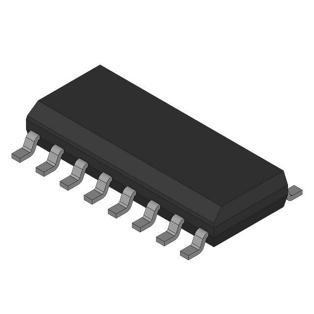
SOIC (14)
8.65 mm × 3.91 mm
PDIP (14)
19.177 mm × 6.35 mm
(1) For all available packages, see the orderable addendum at
the end of the data sheet.
Single-Ended Unity Gain Buffer
1
An IMPORTANT NOTICE at the end of this data sheet addresses availability, warranty, changes, use in safety-critical applications,
intellectual property matters and other important disclaimers. PRODUCTION DATA.
�LMC6484
SNOS675C – AUGUST 2000 – REVISED SEPTEMBER 2015
www.ti.com
Table of Contents
1
2
3
4
5
6
Features ..................................................................
Applications ...........................................................
Description .............................................................
Revision History.....................................................
Pin Configuration and Functions .........................
Specifications.........................................................
6.1
6.2
6.3
6.4
6.5
6.6
6.7
6.8
6.9
6.10
6.11
6.12
6.13
6.14
6.15
1
1
1
2
3
4
Absolute Maximum Ratings ...................................... 4
ESD Ratings.............................................................. 4
Recommended Operating Conditions....................... 4
Thermal Information .................................................. 4
DC Electrical Characteristics for LMC6484AI ........... 5
DC Electrical Characteristics for LMC6484I.............. 7
DC Electrical Characteristics for LMC6484M............ 9
DC Electrical Characteristics for LMC6484AI ......... 11
DC Electrical Characteristics for LMC6484I............ 11
DC Electrical Characteristics for LMC6484M........ 12
AC Electrical Characteristics for LMC6484A ........ 13
AC Electrical Characteristics for LMC6484I.......... 13
AC Electrical Characteristics for LMC6484M........ 14
AC Electrical Characteristics, V+ = 3 V, V− = 0 V . 14
Typical Characteristics .......................................... 15
7
Detailed Description ............................................ 23
7.1
7.2
7.3
7.4
8
Overview .................................................................
Functional Block Diagram .......................................
Feature Description.................................................
Device Functional Modes........................................
23
23
23
24
Application and Implementation ........................ 25
8.1 Application Information............................................ 25
8.2 Typical Application ................................................. 25
8.3 System Examples ................................................... 31
9 Power Supply Recommendations...................... 36
10 Layout................................................................... 36
10.1 Layout Guidelines ................................................. 36
10.2 Layout Example .................................................... 37
11 Device and Documentation Support ................. 38
11.1
11.2
11.3
11.4
11.5
11.6
Device Support......................................................
Documentation Support ........................................
Community Resource............................................
Trademarks ...........................................................
Electrostatic Discharge Caution ............................
Glossary ................................................................
38
38
38
38
38
38
12 Mechanical, Packaging, and Orderable
Information ........................................................... 38
4 Revision History
NOTE: Page numbers for previous revisions may differ from page numbers in the current version.
Changes from Revision B (August 2000) to Revision C
•
2
Page
Added ESD Ratings table, Feature Description section, Device Functional Modes, Application and Implementation
section, Power Supply Recommendations section, Layout section, Device and Documentation Support section, and
Mechanical, Packaging, and Orderable Information section. ................................................................................................ 1
Submit Documentation Feedback
Copyright © 2000–2015, Texas Instruments Incorporated
Product Folder Links: LMC6484
�LMC6484
www.ti.com
SNOS675C – AUGUST 2000 – REVISED SEPTEMBER 2015
5 Pin Configuration and Functions
D or NFF Packages
14-Pin SOIC or PDIP
Top View
Pin Functions
PIN
NO.
NAME
TYPE
DESCRIPTION
1
OUTPUT1
O
Output for Amplifier 1
2
INVERTING INPUT1
I
Inverting input for Amplifier 1
3
NONINVERTING
INPUT1
I
Noninverting input for Amplifier 1
4
V+
P
Positive voltage supply pin
5
NONINTERTING
INPUT2
I
Noninverting input for Amplifier 2
6
INVERTING INPUT2
I
Inverting input for Amplifier 2
7
OUTPUT2
O
Output for Amplifier 2
8
OUTPUT3
O
Output for Amplifier 3
9
INVERTING INPUT3
I
Inverting input for Amplifier 3
10
NONINVERTING
INPUT3
I
Noninverting input for Amplifier 3
11
V–
P
Negative supply voltage pin
12
NONINVERTING
INPUT4
I
Noninverting input for Amplifier 4
13
INVERTING INPUT4
I
Inverting input for Amplifier 4
14
OUTPUT4
O
Output for Amplifier 5
Submit Documentation Feedback
Copyright © 2000–2015, Texas Instruments Incorporated
Product Folder Links: LMC6484
3
�LMC6484
SNOS675C – AUGUST 2000 – REVISED SEPTEMBER 2015
www.ti.com
6 Specifications
6.1 Absolute Maximum Ratings
See (1) (2)
MIN
Differential input voltage
(V−) − 0.3
Voltage at input/output pin
+
MAX
UNIT
±Supply Voltage
(V+) + 0.3
−
V
Supply voltage (V − V )
16
V
Current at input pin (3)
±5
mA
Current at output pin (4) (5)
±30
mA
Current at power supply pin
40
mA
Junction temperature (6)
150
°C
150
°C
−65
Storage temperature, Tstg
(1)
(2)
(3)
(4)
(5)
(6)
Stresses beyond those listed under Absolute Maximum Ratings may cause permanent damage to the device. These are stress ratings
only, which do not imply functional operation of the device at these or any other conditions beyond those indicated under Recommended
Operating Conditions. Exposure to absolute-maximum-rated conditions for extended periods may affect device reliability.
If Military/Aerospace specified devices are required, contact the Texas Instruments Sales Office/Distributors for availability and
specifications.
Limiting input pin current is only necessary for input voltages that exceed absolute maximum input voltage ratings.
Applies to both single supply and split-supply operation. Continuous short circuit operation at elevated ambient temperature can result in
exceeding the maximum allowed junction temperature of 150°C. Output currents in excess of ±30 mA over long term may adversely
affect reliability.
Do not short circuit output to V+, when V+ is greater than 13 V or reliability will be adversely affected.
The maximum power dissipation is a function of TJ(max), RθJA, and TA. The maximum allowable power dissipation at any ambient
temperature is PD = (TJ(max) − TA)/RJθA. All numbers apply for packages soldered directly into a PC board.
6.2 ESD Ratings
V(ESD)
(1)
(2)
Electrostatic discharge
Human body model (HBM), per ANSI/ESDA/JEDEC JS-001 (1) (2)
VALUE
UNIT
±2000
V
JEDEC document JEP155 states that 500-V HBM allows safe manufacturing with a standard ESD control process. Manufacturing with
less than 500-V HBM is possible with the necessary precautions.
Human body model, 1.5-kΩ resistor in series with 100 pF. All pins rated per method 3015.6 of MIL-STD-883. This is a class 2 device
rating.
6.3 Recommended Operating Conditions
over operating free-air temperature range (unless otherwise noted)
Supply voltage, V+
Junction temperature, TJ
MIN
MAX
UNIT
3
15.5
V
LMC6484AM
−55
125
°C
LMC6484AI, LMC6484I
−40
85
°C
6.4 Thermal Information
LMC6484
THERMAL METRIC
RθJA
(1)
4
(1)
Junction-to-ambient thermal resistance
D (SOIC)
NFF (PDIP)
14 PINS
14 PINS
110
70
UNIT
°C/W
For more information about traditional and new thermal metrics, see the Semiconductor and IC Package Thermal Metrics application
report, SPRA953.
Submit Documentation Feedback
Copyright © 2000–2015, Texas Instruments Incorporated
Product Folder Links: LMC6484
�LMC6484
www.ti.com
SNOS675C – AUGUST 2000 – REVISED SEPTEMBER 2015
6.5 DC Electrical Characteristics for LMC6484AI
Unless otherwise specified, all limits specified for TJ = 25°C, V+ = 5 V, V− = 0 V, VCM = VO = V+/2 and RL > 1 M.
PARAMETER
VOS
Input offset
voltage
TCVOS
Input offset
voltage average
drift
IB
Input current (3)
IOS
Input offset
current (3)
CIN
Common-mode
input capacitance
RIN
Input resistance
TYP (2)
MAX (1)
0.11
0.75
At the temperature extremes
1.35
1
4
0.01
At the temperature extremes
2
3
Common-mode
rejection ratio
0 V ≤ VCM ≤ 5 V
V+ = 5 V
At the temperature
extremes
70
+PSRR
Positive power
supply rejection
ratio
5 V ≤ V+ ≤ 15 V
V− = 0 V
VO = 2.5 V
At the temperature
extremes
−PSRR
Negative power
supply rejection
ratio
−5 V ≤ V− ≤ −15 V
V+ = 0 V
VO = −2.5 V
At the temperature
extremes
dB
82
dB
82
dB
67
70
82
dB
67
V− − 0.3
VCM
Input commonmode voltage
range
V+ = 5 V and 15 V
For CMRR ≥ 50 dB
At the temperature
extremes
At the temperature
extremes
Sourcing
Sinking
At the
temperature
extremes
RL = 2 kΩ (4)
AV
Large signal
voltage gain
RL = 600 Ω (3) (4)
At the
temperature
extremes
V/mV
75
V/mV
300
V/mV
48
20
Sinking
(1)
(2)
(3)
(4)
At the
temperature
extremes
666
20
80
Sourcing
V
84
35
13
V
V+ + 0.3
V+
140
At the
temperature
extremes
−0.25
0
V+ + 0.25
pA
Tera Ω
67
70
pA
82
67
At the temperature
extremes
mV
pF
>10
70
UNIT
µV/˚C
0.02
At the temperature extremes
0 V ≤ VCM ≤ 15 V
V+ = 15 V
CMRR
MIN (1)
TEST CONDITIONS
35
V/mV
All limits are specified by testing or statistical analysis.
Typical values represent the most likely parametric normal.
Specified limits are dictated by tester limitations and not device performance. Actual performance is reflected in the typical value.
V+ = 15 V, VCM = 7.5 V and RL connected to 7.5 V. For sourcing tests, 7.5 V ≤ VO ≤ 11.5 V. For sinking tests, 3.5 V ≤ VO ≤ 7.5 V.
Submit Documentation Feedback
Copyright © 2000–2015, Texas Instruments Incorporated
Product Folder Links: LMC6484
5
�LMC6484
SNOS675C – AUGUST 2000 – REVISED SEPTEMBER 2015
www.ti.com
DC Electrical Characteristics for LMC6484AI (continued)
Unless otherwise specified, all limits specified for TJ = 25°C, V+ = 5 V, V− = 0 V, VCM = VO = V+/2 and RL > 1 M.
PARAMETER
TEST CONDITIONS
+
V =5V
RL = 2 kΩ to V+/2
At the temperature
extremes
MIN (1)
TYP (2)
4.8
4.9
0.1
VO
At the temperature
extremes
V
4.24
0.3
V+ = 15 V
RL = 2 kΩ to V+/2
V
14.2
0.16
+
V = 15 V
RL = 600 Ω to V+/2
V
13
0.5
ISC
Output short
circuit current
V+ = 5 V
Sinking,
VO = 5 V
At the temperature
extremes
ISC
IS
(5)
6
Output short
circuit current
V+ = 15 V
Supply current
Sinking,
VO = 12 V (5)
At the temperature
extremes
15
mA
30
mA
22
30
At the temperature
extremes
mA
9.5
28
Sourcing, VO = 0 V
30
mA
24
2
All four amplifiers
V+ = +5 V,
VO = V+/2
At the temperature
extremes
All four amplifiers
V+ = +15 V,
VO = V+/2
At the temperature
extremes
V
20
12
11
At the temperature
extremes
1
1.3
16
V
14.1
At the temperature
extremes
Sourcing, VO = 0 V
0.32
0.45
13.4
V
14.7
At the temperature
extremes
At the temperature
extremes
0.5
0.65
14.4
At the temperature
extremes
V
4.7
At the temperature
extremes
Output swing
0.18
0.24
4.5
UNIT
V
4.7
At the temperature
extremes
V+ = 5 V
RL = 600 Ω to V+/2
MAX (1)
2.8
3.6
2.6
mA
3
3.8
mA
When V+ is greater than 13 V, do not short circuit output to V+ or reliability will be adversely affected.
Submit Documentation Feedback
Copyright © 2000–2015, Texas Instruments Incorporated
Product Folder Links: LMC6484
�LMC6484
www.ti.com
SNOS675C – AUGUST 2000 – REVISED SEPTEMBER 2015
6.6 DC Electrical Characteristics for LMC6484I
Unless otherwise specified, all limits specified for TJ = 25°C, V+ = 5 V, V− = 0 V, VCM = VO = V+/2 and RL > 1 M.
PARAMETER
VOS
Input offset voltage
TCVOS
Input offset voltage
average drift
IB
Input current (3)
IOS
Input offset
current (3)
CIN
Common-mode
input capacitance
RIN
Input resistance
CMRR
Common-mode
rejection ratio
MIN (1)
TEST CONDITIONS
TYP (2)
0.11
At the temperature extremes
1
mV
µV/˚C
pA
4
0.01
At the temperature extremes
pA
2
3
pF
Tera Ω
>10
0 V ≤ VCM ≤ 15 V
V+ = 15 V
0 V ≤ VCM ≤ 5 V
V+ = 5 V
65
At the temperature extremes
65
5 V ≤ V+ ≤ 15 V
Positive power
supply rejection ratio V− = 0 V, VO = 2.5 V At the temperature extremes
65
−5 V ≤ V− ≤ −15 V
Negative power
+
supply rejection ratio V = 0 V, VO = −2.5
V
65
−PSRR
At the temperature extremes
82
82
Input common-mode V = 5 V and 15 V
voltage range
For CMRR ≥ 50 dB
82
dB
62
RL = 2 kΩ
Sinking
At the
temperature
extremes
(4)
At the
temperature
extremes
Sinking
At the
temperature
extremes
RL = 600 Ω (3) (4)
V
666
75
20
50
Sourcing
V+ + 0.3
72
35
Large signal voltage
gain
V
V+
120
Sourcing
−0.25
0
V+ + 0.25
At the
temperature
extremes
dB
82
At the temperature extremes
At the temperature extremes
dB
62
V− − 0.3
+
dB
62
+PSRR
(1)
(2)
(3)
(4)
UNIT
0.02
At the temperature extremes
60
AV
3
3.7
At the temperature extremes
VCM
MAX (1)
300
V/mV
30
15
35
10
All limits are specified by testing or statistical analysis.
Typical values represent the most likely parametric normal.
Specified limits are dictated by tester limitations and not device performance. Actual performance is reflected in the typical value.
V+ = 15 V, VCM = 7.5 V and RL connected to 7.5 V. For sourcing tests, 7.5 V ≤ VO ≤ 11.5 V. For sinking tests, 3.5 V ≤ VO ≤ 7.5 V.
Submit Documentation Feedback
Copyright © 2000–2015, Texas Instruments Incorporated
Product Folder Links: LMC6484
7
�LMC6484
SNOS675C – AUGUST 2000 – REVISED SEPTEMBER 2015
www.ti.com
DC Electrical Characteristics for LMC6484I (continued)
Unless otherwise specified, all limits specified for TJ = 25°C, V+ = 5 V, V− = 0 V, VCM = VO = V+/2 and RL > 1 M.
PARAMETER
TEST CONDITIONS
V+ = 5 V
RL = 2 kΩ to V+/2
At the temperature extremes
MIN (1)
TYP (2)
4.8
4.9
0.1
VO
4.7
0.3
V = 15 V
RL = 2 kΩ to V+/2
At the temperature extremes
14.7
0.16
V = 15 V
RL = 600 Ω to V+/2
At the temperature extremes
14.1
0.5
ISC
ISC
IS
(5)
8
Output short circuit
current
V+ = 15 V
Supply current
Sourcing, VO = 0 V
Sinking,
VO = 5 V
Sourcing, VO = 0 V
Sinking,
VO = 12 V (5)
All four amplifiers
V+ = +5 V
VO = V+/2
All four amplifiers
V+ = +15 V
VO = V+/2
At the temperature extremes
12
At the temperature extremes
9.5
11
28
At the temperature extremes
20
15
mA
30
mA
30
mA
24
2
At the temperature extremes
2.8
3.6
2.6
At the temperature extremes
V
mA
22
30
At the temperature extremes
1
1.3
16
V
V
13
At the temperature extremes
Output short circuit
current
V+ = 5 V
0.32
0.45
13.4
V
V
14.2
At the temperature extremes
+
0.5
0.65
14.4
+
V
V
4.24
At the temperature extremes
Output swing
0.18
0.24
4.5
At the temperature extremes
UNIT
V
4.7
At the temperature extremes
V+ = 5 V
RL = 600 Ω to V+/2
MAX (1)
mA
3
3.8
mA
When V+ is greater than 13 V, do not short circuit output to V+ or reliability will be adversely affected.
Submit Documentation Feedback
Copyright © 2000–2015, Texas Instruments Incorporated
Product Folder Links: LMC6484
�LMC6484
www.ti.com
SNOS675C – AUGUST 2000 – REVISED SEPTEMBER 2015
6.7 DC Electrical Characteristics for LMC6484M
Unless otherwise specified, all limits specified for TJ = 25°C, V+ = 5 V, V− = 0 V, VCM = VO = V+/2 and RL > 1 M.
PARAMETER
VOS
Input offset voltage
TCVOS
Input offset voltage
average drift
IB
Input current (3)
IOS
Input offset
current (3)
CIN
Common-mode
input capacitance
RIN
Input resistance
CMRR
Common-mode
rejection ratio
TEST CONDITIONS
MIN (1)
TYP (2)
0.11
At the temperature extremes
mV
µV/˚C
pA
100
0.01
At the temperature extremes
pA
50
3
pF
Tera Ω
>10
0 V ≤ VCM ≤ 15 V
V+ = 15 V
0 V ≤ VCM ≤ 5 V
V+ = 5 V
−PSRR
−5 V ≤ V− ≤ −15 V
Negative power
+
supply rejection ratio V = 0 V
VO = −2.5 V
65
At the temperature extremes
65
At the temperature extremes
8
+
Input common-mode V = 5 V and 15 V
voltage range
For CMRR ≥ 50 dB
82
dB
82
dB
60
At the temperature extremes
RL = 2 kΩ
(4)
At the
temperature
extremes
Large signal voltage
gain
At the
temperature
extremes
RL = 600 Ω
At the
temperature
extremes
Sinking
At the
temperature
extremes
(3) (4)
V
666
72
75
20
50
Sourcing
V+ + 0.3
V
35
Sinking
V
+
120
Sourcing
−0.25
0
V+ + 0.25
At the temperature extremes
dB
60
65
At the temperature extremes
dB
60
65
At the temperature extremes
82
60
V− − 0.3
(1)
(2)
(3)
(4)
UNIT
0.02
At the temperature extremes
5 V ≤ V+ ≤ 15 V
Positive power
−
supply rejection ratio V = 0 V, VO = 2.5
V
AV
3
3.8
1
+PSRR
VCM
MAX (1)
300
V/mV
30
15
35
10
All limits are specified by testing or statistical analysis.
Typical values represent the most likely parametric normal.
Specified limits are dictated by tester limitations and not device performance. Actual performance is reflected in the typical value.
V+ = 15 V, VCM = 7.5 V and RL connected to 7.5 V. For sourcing tests, 7.5 V ≤ VO ≤ 11.5 V. For sinking tests, 3.5 V ≤ VO ≤ 7.5 V.
Submit Documentation Feedback
Copyright © 2000–2015, Texas Instruments Incorporated
Product Folder Links: LMC6484
9
�LMC6484
SNOS675C – AUGUST 2000 – REVISED SEPTEMBER 2015
www.ti.com
DC Electrical Characteristics for LMC6484M (continued)
Unless otherwise specified, all limits specified for TJ = 25°C, V+ = 5 V, V− = 0 V, VCM = VO = V+/2 and RL > 1 M.
PARAMETER
TEST CONDITIONS
V+ = 5 V
RL = 2 kΩ to V+/2
At the temperature extremes
MIN (1)
TYP (2)
4.8
4.9
0.1
VO
4.7
0.3
V = 15 V
RL = 2 kΩ to V+/2
At the temperature extremes
14.7
0.16
V = 15 V
RL = 600 Ω to V+/2
At the temperature extremes
14.1
0.5
ISC
ISC
IS
(5)
10
Output short circuit
current
V+ = 15 V
Supply current
Sourcing, VO = 0 V
Sinking,
VO = 5 V
Sourcing, VO = 0 V
Sinking,
VO = 12 V (5)
All four amplifiers
V+ = +5 V
VO = V+/2
All four amplifiers
V+ = +15 V,
VO = V+/2
At the temperature extremes
At the temperature extremes
15
mA
30
mA
20
30
30
mA
22
2
At the temperature extremes
2.8
3.8
2.6
At the temperature extremes
V
mA
8
28
At the temperature extremes
20
10
11
At the temperature extremes
1
1.3
16
V
V
13
At the temperature extremes
Output short circuit
current
V+ = 5 V
0.32
0.45
13.4
V
V
14.2
At the temperature extremes
+
0.5
0.65
14.4
+
V
V
4.24
At the temperature extremes
Output swing
0.18
0.24
4.5
At the temperature extremes
UNIT
V
4.7
At the temperature extremes
V+ = 5 V
RL = 600 Ω to V+/2
MAX (1)
mA
3
4
mA
When V+ is greater than 13 V, do not short circuit output to V+ or reliability will be adversely affected.
Submit Documentation Feedback
Copyright © 2000–2015, Texas Instruments Incorporated
Product Folder Links: LMC6484
�LMC6484
www.ti.com
SNOS675C – AUGUST 2000 – REVISED SEPTEMBER 2015
6.8 DC Electrical Characteristics for LMC6484AI
Unless otherwise specified, all limits specified for TJ = 25°C, V+ = 3 V, V− = 0 V, VCM = VO = V+/2 and RL > 1 M.
PARAMETER
TEST CONDITIONS
MIN (1)
TYP (2)
MAX (1)
0.9
VOS
Input offset voltage
TCVOS
Input offset voltage average drift
IB
Input bias current
IOS
Input offset current
CMRR
Common-mode rejection ratio
0 V ≤ VCM ≤ 3 V
64
PSRR
Power supply rejection ratio
3 V ≤ V+ ≤ 15 V, V− = 0 V
68
2
At the temperature extremes
2.7
2
Input common-mode voltage range
For CMRR ≥ 50 dB
µV/˚C
pA
0.01
pA
74
dB
80
dB
V − 0.25
V+
Output swing
RL = 600 Ω to V+/2
IS
(1)
(2)
Supply current
All four
amplifiers
0
V
V+ + 0.25
V
2.8
V
0.2
V
RL = 2 kΩ to V+/2
VO
mV
0.02
−
VCM
UNIT
2.5
2.7
V
0.37
0.6
1.65
2.5
At the temperature
extremes
3
V
mA
All limits are specified by testing or statistical analysis.
Typical values represent the most likely parametric normal.
6.9 DC Electrical Characteristics for LMC6484I
Unless otherwise specified, all limits specified for TJ = 25°C, V+ = 3 V, V− = 0 V, VCM = VO = V+/2 and RL > 1 M.
PARAMETER
TEST CONDITIONS
MIN (1)
TYP (2)
MAX (1)
0.9
3
VOS
Input offset voltage
TCVOS
Input offset voltage average drift
IB
Input bias current
IOS
Input offset current
CMRR
Common-mode rejection ratio
0 V ≤ VCM ≤ 3 V
60
PSRR
Power supply rejection ratio
3 V ≤ V+ ≤ 15 V, V− = 0 V
60
80
VCM
Input common-mode voltage
range
At the temperature extremes
3.7
2
+
V
RL = 2 kΩ to V+/2
VO
Output swing
2.5
RL = 600 Ω to V+/2
IS
(1)
(2)
Supply current
All four amplifiers
At the temperature
extremes
mV
µV/˚C
0.02
pA
0.01
pA
74
dB
V− − 0.25
For CMRR ≥ 50 dB
UNIT
dB
0
+
V
V + 0.25
V
2.8
V
0.2
V
2.7
V
0.37
0.6
1.65
2.5
3
V
mA
All limits are specified by testing or statistical analysis.
Typical values represent the most likely parametric normal.
Submit Documentation Feedback
Copyright © 2000–2015, Texas Instruments Incorporated
Product Folder Links: LMC6484
11
�LMC6484
SNOS675C – AUGUST 2000 – REVISED SEPTEMBER 2015
www.ti.com
6.10 DC Electrical Characteristics for LMC6484M
Unless otherwise specified, all limits specified for TJ = 25°C, V+ = 3 V, V− = 0 V, VCM = VO = V+/2 and RL > 1 M.
PARAMETER
TEST CONDITIONS
MIN (1)
TYP (2)
0.9
MAX (1)
3
UNIT
VOS
Input offset voltage
TCVOS
Input offset voltage average
drift
IB
Input bias current
0.02
pA
IOS
Input offset current
0.01
pA
CMRR
Common-mode rejection ratio
74
dB
PSRR
Power supply rejection ratio
VCM
Input common-mode voltage
range
At the temperature extremes
3.8
2
0 V ≤ VCM ≤ 3 V
60
−
+
3 V ≤ V ≤ 15 V, V = 0 V
60
For CMRR ≥ 50 dB
V+
RL = 2 kΩ to V+/2
VO
Output swing
2.5
RL = 600 Ω to V+/2
IS
(1)
(2)
12
Supply current
All four amplifiers
At the temperature
extremes
µV/˚C
80
V− − 0.25
mV
dB
0
V
V+ + 0.25
V
2.8
V
0.2
V
2.7
V
0.37
0.6
1.65
2.5
3.2
V
mA
All limits are specified by testing or statistical analysis.
Typical values represent the most likely parametric normal.
Submit Documentation Feedback
Copyright © 2000–2015, Texas Instruments Incorporated
Product Folder Links: LMC6484
�LMC6484
www.ti.com
SNOS675C – AUGUST 2000 – REVISED SEPTEMBER 2015
6.11 AC Electrical Characteristics for LMC6484A
Unless otherwise specified, all limits specified for TJ = 25°C, V+ = 5 V, V− = 0 V, VCM = VO = V+ / 2 and RL > 1 M.
PARAMETER
SR
Slew rate (3)
GBW
Gain-bandwidth
product
Фm
Gm
TEST CONDITIONS
At the temperature extremes
MIN (1)
TYP (2)
1
1.3
V+ = 15 V
1.5
MHz
Phase margin
50
Deg
Gain margin
15
dB
150
dB
37
nV√Hz
0.03
pA√Hz
en
Input-referred voltage
noise
f = 1 kHz, VCM = 1 V
in
Input-referred current
noise
f = 1 kHz
T.H.D.
Total harmonic
distortion
f = 1 kHz, AV = −2,
RL = 10 kΩ, VO = 4.1 VPP
0.01%
f = 10 kHz, AV = −2,
RL = 10 kΩ, VO = 8.5 VPP,
V+ = 10 V
0.01%
(4)
UNIT
V/µs
0.7
Amplifier-to-amplifier
isolation (4)
(1)
(2)
(3)
MAX (1)
All limits are specified by testing or statistical analysis.
Typical values represent the most likely parametric normal.
V+ = 15 V. Connected as voltage follower with 10-V step input. Number specified is the slower of either the positive or negative slew
rates.
Input referred, V+ = 15 V and RL = 100 kΩ connected to 7.5 V. Each amplifier excited in turn with 1 kHz to produce VO = 12 VPP.
6.12 AC Electrical Characteristics for LMC6484I
Unless otherwise specified, all limits specified for TJ = 25°C, V+ = 5 V, V− = 0 V, VCM = VO = V+/2 and RL > 1M.
PARAMETER
TEST CONDITIONS
MIN (1)
TYP (2)
0.9
1.3
MAX (1)
UNIT
SR
Slew rate (3)
GBW
Gain-bandwidth product
1.5
MHz
Фm
Phase margin
50
Deg
Gm
Gain margin
15
dB
150
dB
37
nV√Hz
0.03
pA√Hz
At the temperature extremes
V+ = 15 V
Amplifier-to-amplifier
isolation (4)
0.63
en
Input-referred voltage noise
f = 1 kHz, VCM = 1 V
in
Input-referred current noise
f = 1 kHz
T.H.D.
Total harmonic distortion
f = 1 kHz, AV = −2,
RL = 10 kΩ, VO = 4.1 VPP
0.01%
f = 10 kHz, AV = −2,
RL = 10 kΩ, VO = 8.5 VPP,
V+ = 10 V
0.01%
(1)
(2)
(3)
(4)
V/µs
All limits are specified by testing or statistical analysis.
Typical values represent the most likely parametric normal.
V+ = 15 V. Connected as Voltage Follower with 10-V step input. Number specified is the slower of either the positive or negative slew
rates.
Input referred, V+ = 15 V and RL = 100 kΩ connected to 7.5 V. Each amp excited in turn with 1 kHz to produce VO = 12 VPP.
Submit Documentation Feedback
Copyright © 2000–2015, Texas Instruments Incorporated
Product Folder Links: LMC6484
13
�LMC6484
SNOS675C – AUGUST 2000 – REVISED SEPTEMBER 2015
www.ti.com
6.13 AC Electrical Characteristics for LMC6484M
Unless otherwise specified, all limits specified for TJ = 25°C, V+ = 5 V, V− = 0 V, VCM = VO = V+/2 and RL > 1M.
PARAMETER
SR
Slew rate (3)
GBW
Gain-bandwidth product
Фm
Phase margin
Gm
Gain margin
TEST CONDITIONS
At the temperature extremes
MIN (1)
TYP (2)
0.9
1.3
Amplifier-to-amplifier isolation (4)
Input-referred voltage noise
f = 1 kHz, VCM = 1 V
in
Input-referred current noise
f = 1 kHz
T.H.D.
(1)
(2)
(3)
(4)
Total harmonic distortion
UNIT
V/µs
0.54
V+ = 15 V
en
MAX (1)
1.5
MHz
50
Deg
15
dB
150
dB
37
nV√Hz
0.03
pA√Hz
f = 1 kHz, AV = −2,
RL = 10 kΩ, VO = 4.1 VPP
0.01%
f = 10 kHz, AV = −2,
RL = 10 kΩ, VO = 8.5 VPP,
V+ = 10 V
0.01%
All limits are specified by testing or statistical analysis.
Typical values represent the most likely parametric normal.
V+ = 15 V. Connected as Voltage Follower with 10-V step input. Number specified is the slower of either the positive or negative slew
rates.
Input referred, V+ = 15 V and RL = 100 kΩ connected to 7.5 V. Each amplifier excited in turn with 1 kHz to produce VO = 12 VPP.
6.14 AC Electrical Characteristics, V+ = 3 V, V− = 0 V
Unless otherwise specified, V+ = 3 V, V− = 0 V, VCM = VO = V+/2 and RL > 1M
PARAMETER
SR
Slew rate (3)
GBW
Gain-bandwidth product
T.H.D.
(1)
(2)
(3)
14
Total harmonic distortion
TEST CONDITIONS
f = 10 kHz, AV = −2,
RL = 10 kΩ, VO = 2 VPP
LMC6484AI, LMC6484I, LMC6484M
MIN (1)
TYP (2)
MAX (1)
UNIT
0.9
V/µs
1
MHz
0.01%
All limits are specified by testing or statistical analysis.
Typical values represent the most likely parametric normal.
Connected as voltage follower with 2-V step input. Number specified is the slower of either the positive or negative slew rates.
Submit Documentation Feedback
Copyright © 2000–2015, Texas Instruments Incorporated
Product Folder Links: LMC6484
�LMC6484
www.ti.com
SNOS675C – AUGUST 2000 – REVISED SEPTEMBER 2015
6.15 Typical Characteristics
VS = 15 V, Single Supply, TA = 25°C (unless otherwise specified)
Figure 1. Supply Current vs Supply Voltage
Figure 2. Input Current vs Temperature
Figure 3. Sourcing Current vs Output Voltage
Figure 4. Sourcing Current vs Output Voltage
Figure 5. Sourcing Current vs Output Voltage
Figure 6. Sinking Current vs Output Voltage
Submit Documentation Feedback
Copyright © 2000–2015, Texas Instruments Incorporated
Product Folder Links: LMC6484
15
�LMC6484
SNOS675C – AUGUST 2000 – REVISED SEPTEMBER 2015
www.ti.com
Typical Characteristics (continued)
VS = 15 V, Single Supply, TA = 25°C (unless otherwise specified)
Figure 7. Sinking Current vs Output Voltage
Figure 8. Sinking Current vs Output Voltage
.
16
Figure 9. Output Voltage Swing vs Supply Voltage
Figure 10. Input Voltage Noise vs Frequency
Figure 11. Input Voltage Noise vs Input Voltage
Figure 12. Input Voltage Noise vs Input Voltage
Submit Documentation Feedback
Copyright © 2000–2015, Texas Instruments Incorporated
Product Folder Links: LMC6484
�LMC6484
www.ti.com
SNOS675C – AUGUST 2000 – REVISED SEPTEMBER 2015
Typical Characteristics (continued)
VS = 15 V, Single Supply, TA = 25°C (unless otherwise specified)
Figure 13. Input Voltage Noise vs Input Voltage
Figure 14. Crosstalk Rejection vs Frequency
Figure 15. Crosstalk Rejection vs Frequency
Figure 16. Positive PSRR vs Frequency
Figure 17. Negative PSRR vs Frequency
Figure 18. CMRR vs Frequency
Submit Documentation Feedback
Copyright © 2000–2015, Texas Instruments Incorporated
Product Folder Links: LMC6484
17
�LMC6484
SNOS675C – AUGUST 2000 – REVISED SEPTEMBER 2015
www.ti.com
Typical Characteristics (continued)
VS = 15 V, Single Supply, TA = 25°C (unless otherwise specified)
18
Figure 19. CMRR vs Input Voltage
Figure 20. CMRR vs Input Voltage
Figure 21. CMRR vs Input Voltage
Figure 22. ΔVOS vs CMR
Figure 23. ΔVOS vs CMR
Figure 24. Input Voltage vs Output Voltage
Submit Documentation Feedback
Copyright © 2000–2015, Texas Instruments Incorporated
Product Folder Links: LMC6484
�LMC6484
www.ti.com
SNOS675C – AUGUST 2000 – REVISED SEPTEMBER 2015
Typical Characteristics (continued)
VS = 15 V, Single Supply, TA = 25°C (unless otherwise specified)
Figure 25. Input Voltage vs Output Voltage
Figure 26. Open Loop Frequency Response
Figure 27. Noninverting Large Signal Pulse Response
Figure 28. Noninverting Large Signal Pulse Response
Figure 29. Noninverting Large Signal Pulse Response
Figure 30. Noninverting Small Signal Pulse Response
Submit Documentation Feedback
Copyright © 2000–2015, Texas Instruments Incorporated
Product Folder Links: LMC6484
19
�LMC6484
SNOS675C – AUGUST 2000 – REVISED SEPTEMBER 2015
www.ti.com
Typical Characteristics (continued)
VS = 15 V, Single Supply, TA = 25°C (unless otherwise specified)
20
Figure 31. Noninverting Small Signal Pulse Response
Figure 32. Noninverting Small Signal Pulse Response
Figure 33. Inverting Large Signal Pulse Response
Figure 34. Inverting Large Signal Pulse Response
Figure 35. Inverting Large Signal Pulse Response
Figure 36. Inverting Small Signal Pulse Response
Submit Documentation Feedback
Copyright © 2000–2015, Texas Instruments Incorporated
Product Folder Links: LMC6484
�LMC6484
www.ti.com
SNOS675C – AUGUST 2000 – REVISED SEPTEMBER 2015
Typical Characteristics (continued)
VS = 15 V, Single Supply, TA = 25°C (unless otherwise specified)
Figure 37. Inverting Small Signal Pulse Response
Figure 38. Inverting Small Signal Pulse Response
Figure 39. Stability vs Capacitive Load
Figure 40. Stability vs Capacitive Load
Figure 41. Stability vs Capacitive Load
Figure 42. Stability vs Capacitive Load
Submit Documentation Feedback
Copyright © 2000–2015, Texas Instruments Incorporated
Product Folder Links: LMC6484
21
�LMC6484
SNOS675C – AUGUST 2000 – REVISED SEPTEMBER 2015
www.ti.com
Typical Characteristics (continued)
VS = 15 V, Single Supply, TA = 25°C (unless otherwise specified)
Figure 43. Stability vs Capacitive Load
22
Submit Documentation Feedback
Figure 44. Stability vs Capacitive Load
Copyright © 2000–2015, Texas Instruments Incorporated
Product Folder Links: LMC6484
�LMC6484
www.ti.com
SNOS675C – AUGUST 2000 – REVISED SEPTEMBER 2015
7 Detailed Description
7.1 Overview
The LMC6484C is a quad operational amplifier that offers a low cost, low power solution for applications
requiring multiple operational amplifier stages and rail-to-rail operation. It supports a wide supply range (3 V to 15
V) and excellent amplifier-to-amplifer isolation (150 dB typical). It is ideal for battery-powered signal acquisition
systems requiring highly integrated solutions to achieve efficient layout.
7.2 Functional Block Diagram
7.3 Feature Description
7.3.1 Amplifier Topology
The LMC6484 incorporates specially designed wide-compliance range current mirrors and the body effect to
extend input common-mode range to each supply rail. Complementary paralleled differential input stages, like the
type used in other CMOS and bipolar rail-to-rail input amplifiers, were not used because of their inherent
accuracy problems due to CMRR, crossover distortion, and open-loop gain variation.
The input stage design of the LMC6484 is complemented by an output stage capable of rail-to-rail output swing
even when driving a large load. Rail-to-rail output swing is obtained by taking the output directly from the internal
integrator instead of an output buffer stage.
7.3.2 Input Common-Mode Voltage Range
Unlike Bi-FET amplifier designs, the LMC6484 does not exhibit phase inversion when an input voltage exceeds
the negative supply voltage. Figure 46 shows an input voltage exceeding both supplies with no resulting phase
inversion on the output.
Figure 45. An Input Voltage Signal Exceeds the LMC6484
Power Supply Voltages With No Output Phase Inversion
The absolute maximum input voltage is 300 mV beyond either supply rail at room temperature. Voltages greatly
exceeding this absolute maximum rating, as in Figure 46, can cause excessive current to flow in or out of the
input pins possibly affecting reliability.
Submit Documentation Feedback
Copyright © 2000–2015, Texas Instruments Incorporated
Product Folder Links: LMC6484
23
�LMC6484
SNOS675C – AUGUST 2000 – REVISED SEPTEMBER 2015
www.ti.com
Feature Description (continued)
Figure 46. A ±7.5V Input Signal Greatly Exceeds the 3-V
Supply in Figure 47 Causing No Phase Inversion Due to RI
Applications that exceed this rating must externally limit the maximum input current to ±5 mA with an input
resistor as shown in Figure 47.
Figure 47. RI Input Current Protection for Voltages Exceeding the Supply Voltage
7.3.3 Rail-to-Rail Output
The approximated output resistance of the LMC6484 is 180-Ω sourcing and 130-Ω sinking at VS = 3 V and 110-Ω
sourcing and 83-Ω sinking at VS = 5 V. Using the calculated output resistance, maximum output voltage swing
can be estimated as a function of load.
7.4 Device Functional Modes
The LMC6482 may be used in applications where each amplifier channel is used independently, or in
applications in which the channels are cascaded. See Typical Application for more information.
24
Submit Documentation Feedback
Copyright © 2000–2015, Texas Instruments Incorporated
Product Folder Links: LMC6484
�LMC6484
www.ti.com
SNOS675C – AUGUST 2000 – REVISED SEPTEMBER 2015
8 Application and Implementation
NOTE
Information in the following applications sections is not part of the TI component
specification, and TI does not warrant its accuracy or completeness. TI’s customers are
responsible for determining suitability of components for their purposes. Customers should
validate and test their design implementation to confirm system functionality.
8.1 Application Information
8.1.1 Upgrading Applications
The LMC6484 quads and LMC6482 duals have industry standard pin outs to retrofit existing applications.
System performance can be greatly increased by the features of the LMC6484. The key benefit of designing in
the LMC6484 is increased linear signal range. Most operational amplifiers have limited input common-mode
ranges. Signals that exceed this range generate a non-linear output response that persists long after the input
signal returns to the common-mode range.
Linear signal range is vital in applications such as filters where signal peaking can exceed input common-mode
ranges resulting in output phase inversion or severe distortion.
8.1.2 Spice Macromodel
A
•
•
•
•
•
spice macromodel is available for the LMC6484. This model includes accurate simulation of the following:
Input common-mode voltage range
Frequency and transient response
GBW dependence on loading conditions
Quiescent and dynamic supply current
Output swing dependence on loading conditions
and many more characteristics as listed on the macromodel disk.
Contact your local Texas Instruments sales office to obtain an operational amplifier spice model library disk.
8.2 Typical Application
RF
CF
±
RO
VOUT
VIN
+
CL
Figure 48. Unity Gain Buffer for High-Capacitive Loads
Submit Documentation Feedback
Copyright © 2000–2015, Texas Instruments Incorporated
Product Folder Links: LMC6484
25
�LMC6484
SNOS675C – AUGUST 2000 – REVISED SEPTEMBER 2015
www.ti.com
Typical Application (continued)
8.2.1 Design Requirements
• For best performance, ensure that the input voltage swing is between V+ and V-.
• Ensure that the input does not exceed the common-mode input range.
• To reduce the risk of de-stabilizing the output, use resistive isolation on the output when driving capacitive
loads (see Capacitive Load Compensation).
• When large feedback resistors are used, it may be necessary to compensate for parasitic capacitance on the
input (see Compensating for Input Capacitance).
8.2.2 Detailed Design Procedure
8.2.2.1 Capacitive Load Compensation
The LMC6484 can typically directly drive a 100-pF load with VS = 15 V at unity gain without oscillating. The unity
gain follower is the most sensitive configuration. Direct capacitive loading reduces the phase margin of
operational amplifiers. The combination of the output impedance of the operational amplifier and the capacitive
load induces phase lag. This results in either an under-damped pulse response or oscillation.
Capacitive load compensation can be accomplished using resistive isolation as shown in Figure 49. This simple
technique is useful for isolating the capacitive input of multiplexers and A/D converters.
Figure 49. Resistive Isolation of a 330-pF Capacitive Load
Figure 50. Pulse Response of the LMC6484 Circuit in Figure 49
Improved frequency response is achieved by indirectly driving capacitive loads as shown in Figure 51.
26
Submit Documentation Feedback
Copyright © 2000–2015, Texas Instruments Incorporated
Product Folder Links: LMC6484
�LMC6484
www.ti.com
SNOS675C – AUGUST 2000 – REVISED SEPTEMBER 2015
Typical Application (continued)
Figure 51. LMC6484 Noninverting Amplifier, Compensated to Handle a 330-pF Capacitive Load
R1 and C1 serve to counteract the loss of phase margin by feeding forward the high-frequency component of the
output signal back to the inverting input of the amplifier, thereby preserving phase margin in the overall feedback
loop. The values of R1 and C1 are experimentally determined for the desired pulse response. The resulting pulse
response can be seen in Figure 52.
Figure 52. Pulse Response of LMC6484 Circuit in Figure 51
8.2.2.2 Compensating for Input Capacitance
It is quite common to use large values of feedback resistance with amplifiers that have ultra-low input current,
like the LMC6484. Large feedback resistors can react with small values of input capacitance due to transducers,
photodiodes, and circuit board parasitics to reduce phase margins.
Submit Documentation Feedback
Copyright © 2000–2015, Texas Instruments Incorporated
Product Folder Links: LMC6484
27
�LMC6484
SNOS675C – AUGUST 2000 – REVISED SEPTEMBER 2015
www.ti.com
Typical Application (continued)
Figure 53. Canceling the Effect of Input Capacitance
The effect of input capacitance can be compensated for by adding a feedback capacitor. The feedback capacitor
(as in Figure 53), Cf, is first estimated by Equation 1:
1
1
³
2pR1 CIN 2pR2 Cf
or
R1 CIN £ R2 Cf
(1)
which typically provides significant overcompensation. Printed circuit board stray capacitance may be larger or
smaller than that of a breadboard, so the actual optimum value for Cf may be different. The values of Cf should
be checked on the actual circuit. (Refer to the LMC660 Quad CMOS Amplifier data sheet (SNOSBZ3) for a more
detailed discussion.)
8.2.2.3 Offset Voltage Adjustment
Offset voltage adjustment circuits are illustrated in Figure 54 and Figure 55. Large value resistances and
potentiometers are used to reduce power consumption while providing typically ±2.5 mV of adjustment range,
referred to the input, for both configurations with VS = ±5 V.
Figure 54. Inverting Configuration
Offset Voltage Adjustment
28
Figure 55. Noninverting Configuration
Offset Voltage Adjustment
Submit Documentation Feedback
Copyright © 2000–2015, Texas Instruments Incorporated
Product Folder Links: LMC6484
�LMC6484
www.ti.com
SNOS675C – AUGUST 2000 – REVISED SEPTEMBER 2015
Typical Application (continued)
8.2.3 Application Curves
Figure 56. Open Loop Frequency Response
Figure 57. Open Loop Frequency Response vs
Temperature
Figure 58. Maximum Output Swing vs Frequency
Figure 59. Gain and Phase vs Capacitive Load
Figure 60. Gain and Phase vs Capacitive Load
Figure 61. Open Loop Output Impedance vs Frequency
Submit Documentation Feedback
Copyright © 2000–2015, Texas Instruments Incorporated
Product Folder Links: LMC6484
29
�LMC6484
SNOS675C – AUGUST 2000 – REVISED SEPTEMBER 2015
www.ti.com
Typical Application (continued)
Figure 62. Open Loop Output Impedance vs Frequency
30
Submit Documentation Feedback
Figure 63. Slew Rate vs Supply Voltage
Copyright © 2000–2015, Texas Instruments Incorporated
Product Folder Links: LMC6484
�LMC6484
www.ti.com
SNOS675C – AUGUST 2000 – REVISED SEPTEMBER 2015
8.3 System Examples
Figure 64. Half-Wave Rectifier with Input Current Protection (RI)
Figure 65. Half-Wave Rectifier Waveform
The circuit in Figure 64 uses a single supply to half wave rectify a sinusoid centered about ground. RI limits
current into the amplifier caused by the input voltage exceeding the supply voltage. Full wave rectification is
provided by the circuit in Figure 66.
Figure 66. Full Wave Rectifier with Input Current Protection (RI)
Submit Documentation Feedback
Copyright © 2000–2015, Texas Instruments Incorporated
Product Folder Links: LMC6484
31
�LMC6484
SNOS675C – AUGUST 2000 – REVISED SEPTEMBER 2015
www.ti.com
System Examples (continued)
Figure 67. Full Wave Rectifier Waveform
Figure 68. Large Compliance Range Current Source
Figure 69. Positive Supply Current Sense
32
Submit Documentation Feedback
Copyright © 2000–2015, Texas Instruments Incorporated
Product Folder Links: LMC6484
�LMC6484
www.ti.com
SNOS675C – AUGUST 2000 – REVISED SEPTEMBER 2015
System Examples (continued)
Figure 70. Low Voltage Peak Detector with Rail-to-Rail Peak Capture Range
In Figure 70 dielectric absorption and leakage is minimized by using a polystyrene or polyethylene hold
capacitor. The droop rate is primarily determined by the value of CH and diode leakage current. The ultra-low
input current of the LMC6484 has a negligible effect on droop.
Figure 71. Rail-to-Rail Sample and Hold
The high CMRR (85 dB) of the LMC6484 allows excellent accuracy throughout the rail-to-rail dynamic capture
range of the circuit.
1
R1 = R2, C1 = C2; f =
1
C2
R2
2
C1
R1
; DF =
2 pR1C1
Figure 72. Rail-to-Rail Single Supply Low Pass Filter
The low pass filter circuit in Figure 72 can be used as an anti-aliasing filter with the same voltage supply as the
A/D converter. Filter designs can also take advantage of the LMC6484 ultra-low input current. The ultra-low input
current yields negligible offset error even when large value resistors are used, which allows the use of smaller
valued capacitors which take less board space and cost less.
Submit Documentation Feedback
Copyright © 2000–2015, Texas Instruments Incorporated
Product Folder Links: LMC6484
33
�LMC6484
SNOS675C – AUGUST 2000 – REVISED SEPTEMBER 2015
www.ti.com
System Examples (continued)
8.3.1 Data Acquisition Systems
Low power, single supply data acquisition system solutions are provided by buffering the ADC12038 with the
LMC6484 (Figure 73). Capable of using the full supply range, the LMC6484 does not require input signals to be
scaled down to meet limited common-mode voltage ranges. The LMC6484 CMRR of 82 dB maintains integral
linearity of a 12-bit data acquisition system to ±0.325 LSB. Other rail-to-rail input amplifiers with only 50 dB of
CMRR will degrade the accuracy of the data acquisition system to only 8 bits.
Figure 73. Operating from the Same Supply Voltage, the
LMC6484 Buffers the ADC12038 Maintaining Excellent Accuracy
34
Submit Documentation Feedback
Copyright © 2000–2015, Texas Instruments Incorporated
Product Folder Links: LMC6484
�LMC6484
www.ti.com
SNOS675C – AUGUST 2000 – REVISED SEPTEMBER 2015
System Examples (continued)
8.3.2 Instrumentation Circuits
The LMC6484 has the high input impedance, large common-mode range and high CMRR needed for designing
instrumentation circuits. Instrumentation circuits designed with the LMC6484 can reject a larger range of
common-mode signals than most in-amps. This makes instrumentation circuits designed with the LMC6484 an
excellent choice for noisy or industrial environments. Other applications that benefit from these features include
analytic medical instruments, magnetic field detectors, gas detectors, and silicon-based transducers.
A small valued potentiometer is used in series with Rg to set the differential gain of the 3-opamp instrumentation
circuit in Figure 74. This combination is used instead of one large valued potentiometer to increase gain trim
accuracy and reduce error due to vibration.
Figure 74. Low-Power 3-Opamp Instrumentation Amplifier
A 2-opamp instrumentation amplifier designed for a gain of 100 is shown in Figure 75. Low sensitivity trimming is
made for offset voltage, CMRR and gain. Low cost and low power consumption are the main advantages of this
2-opamp circuit.
Higher frequency and larger common-mode range applications are best facilitated by a 3-opamp instrumentation
amplifier.
Figure 75. Low-Power 2-Opamp Instrumentation Amplifier
Submit Documentation Feedback
Copyright © 2000–2015, Texas Instruments Incorporated
Product Folder Links: LMC6484
35
�LMC6484
SNOS675C – AUGUST 2000 – REVISED SEPTEMBER 2015
www.ti.com
9 Power Supply Recommendations
The LMC6482 can be operated over a supply range of 3 V to 15 V. To achieve noise immunity as appropriate to
the application, it is important to use good printed circuit board layout practices for power supply rails and planes,
as well as using bypass capacitors connected between the power supply pins and ground.
10 Layout
10.1 Layout Guidelines
10.1.1 Printed-Circuit-Board Layout for High-Impedance Work
It is generally recognized that any circuit which must operate with less than 1000 pA of leakage current requires
special layout of the PC board. when one wishes to take advantage of the ultra-low input current of the
LMC6484, typically less than 20 fA, it is essential to have an excellent layout. Fortunately, the techniques of
obtaining low leakages are quite simple. First, the user must not ignore the surface leakage of the PC board,
even though it may sometimes appear accept- ably low, because under conditions of high humidity or dust or
contamination, the surface leakage will be appreciable.
To minimize the effect of any surface leakage, lay out a ring of foil completely surrounding the LMC6484 inputs
and the terminals of capacitors, diodes, conductors, resistors, relay terminals, etc., connected to the operational
amplifier inputs, as in Figure 78. To have a significant effect, guard rings should be placed in both the top and
bottom of the PC board. This PC foil must then be connected to a voltage which is at the same voltage as the
amplifier inputs, since no leakage current can flow between two points at the same potential. For example, a PC
board trace-to-pad resistance of 1012, which is normally considered a very large resistance, could leak 5 pA if
the trace were a 5-V bus adjacent to the pad of the input. This would cause a 250 times degradation from the
actual performance of the LMC6484. However, if a guard ring is held within 5 mV of the inputs, then even a
resistance of 1011 would cause only 0.05 pA of leakage current. See Figure 76 for typical connections of guard
rings for standard operational amplifier configurations.
Figure 76. Typical Connections of Guard Rings
The designer should be aware that when it is inappropriate to lay out a PC board for the sake of just a few
circuits, there is another technique which is even better than a guard ring on a PC board: Do not insert the input
pin of the amplifier into the board at all, but bend it up in the air and use only air as an insulator. Air is an
excellent insulator. In this case you may have to forego some of the advantages of PC board construction, but
the advantages are sometimes well worth the effort of using point-to-point up-in-the-air wiring. See Figure 77.
Note:
(Input pins are lifted out of PC board and soldered directly to components. All other pins connected to PC board.)
Figure 77. Air Wiring
36
Submit Documentation Feedback
Copyright © 2000–2015, Texas Instruments Incorporated
Product Folder Links: LMC6484
�LMC6484
www.ti.com
SNOS675C – AUGUST 2000 – REVISED SEPTEMBER 2015
10.2 Layout Example
Figure 78. Example of Guard Ring in PCB Layout
Submit Documentation Feedback
Copyright © 2000–2015, Texas Instruments Incorporated
Product Folder Links: LMC6484
37
�LMC6484
SNOS675C – AUGUST 2000 – REVISED SEPTEMBER 2015
www.ti.com
11 Device and Documentation Support
11.1 Device Support
For the LMC6584 PSpice model, see SNOM165.
11.2 Documentation Support
11.2.1 Related Documentation
For related documentation, see the following:
• LMC6482 CMOS Dual Rail-To-Rail Input and Output Operational Amplifier (SNOS674)
• LMC660 CMOS Quad Operational Amplifier (SNOSBZ3)
.
11.3 Community Resource
The following links connect to TI community resources. Linked contents are provided "AS IS" by the respective
contributors. They do not constitute TI specifications and do not necessarily reflect TI's views; see TI's Terms of
Use.
TI E2E™ Online Community TI's Engineer-to-Engineer (E2E) Community. Created to foster collaboration
among engineers. At e2e.ti.com, you can ask questions, share knowledge, explore ideas and help
solve problems with fellow engineers.
Design Support TI's Design Support Quickly find helpful E2E forums along with design support tools and
contact information for technical support.
11.4 Trademarks
E2E is a trademark of Texas Instruments.
All other trademarks are the property of their respective owners.
11.5 Electrostatic Discharge Caution
These devices have limited built-in ESD protection. The leads should be shorted together or the device placed in conductive foam
during storage or handling to prevent electrostatic damage to the MOS gates.
11.6 Glossary
SLYZ022 — TI Glossary.
This glossary lists and explains terms, acronyms, and definitions.
12 Mechanical, Packaging, and Orderable Information
The following pages include mechanical, packaging, and orderable information. This information is the most
current data available for the designated devices. This data is subject to change without notice and revision of
this document. For browser-based versions of this data sheet, refer to the left-hand navigation.
38
Submit Documentation Feedback
Copyright © 2000–2015, Texas Instruments Incorporated
Product Folder Links: LMC6484
�PACKAGE OPTION ADDENDUM
www.ti.com
6-Feb-2020
PACKAGING INFORMATION
Orderable Device
Status
(1)
Package Type Package Pins Package
Drawing
Qty
Eco Plan
Lead/Ball Finish
MSL Peak Temp
(2)
(6)
(3)
Op Temp (°C)
Device Marking
(4/5)
LMC6484AIM
NRND
SOIC
D
14
55
TBD
Call TI
Call TI
-40 to 85
LMC6484
AIM
LMC6484AIM/NOPB
ACTIVE
SOIC
D
14
55
Green (RoHS
& no Sb/Br)
SN
Level-1-260C-UNLIM
-40 to 85
LMC6484
AIM
LMC6484AIMX
NRND
SOIC
D
14
2500
TBD
Call TI
Call TI
-40 to 85
LMC6484
AIM
LMC6484AIMX/NOPB
ACTIVE
SOIC
D
14
2500
Green (RoHS
& no Sb/Br)
SN
Level-1-260C-UNLIM
-40 to 85
LMC6484
AIM
LMC6484AIN/NOPB
ACTIVE
PDIP
NFF
14
25
Green (RoHS
& no Sb/Br)
SN
Level-1-NA-UNLIM
-40 to 85
LMC6484AIN
LMC6484IM
NRND
SOIC
D
14
55
TBD
Call TI
Call TI
-40 to 85
LMC6484IM
LMC6484IM/NOPB
ACTIVE
SOIC
D
14
55
Green (RoHS
& no Sb/Br)
SN
Level-1-260C-UNLIM
-40 to 85
LMC6484IM
LMC6484IMX
NRND
SOIC
D
14
2500
TBD
Call TI
Call TI
-40 to 85
LMC6484IM
LMC6484IMX/NOPB
ACTIVE
SOIC
D
14
2500
Green (RoHS
& no Sb/Br)
SN
Level-1-260C-UNLIM
-40 to 85
LMC6484IM
LMC6484IN/NOPB
ACTIVE
PDIP
NFF
14
25
Green (RoHS
& no Sb/Br)
SN
Level-1-NA-UNLIM
-40 to 85
LMC6484IN
(1)
The marketing status values are defined as follows:
ACTIVE: Product device recommended for new designs.
LIFEBUY: TI has announced that the device will be discontinued, and a lifetime-buy period is in effect.
NRND: Not recommended for new designs. Device is in production to support existing customers, but TI does not recommend using this part in a new design.
PREVIEW: Device has been announced but is not in production. Samples may or may not be available.
OBSOLETE: TI has discontinued the production of the device.
(2)
RoHS: TI defines "RoHS" to mean semiconductor products that are compliant with the current EU RoHS requirements for all 10 RoHS substances, including the requirement that RoHS substance
do not exceed 0.1% by weight in homogeneous materials. Where designed to be soldered at high temperatures, "RoHS" products are suitable for use in specified lead-free processes. TI may
reference these types of products as "Pb-Free".
RoHS Exempt: TI defines "RoHS Exempt" to mean products that contain lead but are compliant with EU RoHS pursuant to a specific EU RoHS exemption.
Green: TI defines "Green" to mean the content of Chlorine (Cl) and Bromine (Br) based flame retardants meet JS709B low halogen requirements of


 工商网监
湘ICP备2023018690号
工商网监
湘ICP备2023018690号
