LMD18201
www.ti.com
SNVS092D – APRIL 1998 – REVISED APRIL 2013
LMD18201 3A, 55V H-Bridge
Check for Samples: LMD18201
FEATURES
APPLICATIONS
•
•
•
•
•
•
•
•
•
•
•
•
•
•
•
1
2
Delivers up to 3A Continuous Output
Operates at Supply Voltages up to 55V
Low RDS(ON) Typically 0.33Ω per Switch at 3A
TTL and CMOS Compatible Inputs
No “Shoot-Through” Current
Thermal Warning Flag Output at 145°C
Thermal Shutdown (Outputs Off) at 170°C
Internal Clamp Diodes
Shorted Load Protection
Internal Charge Pump with External Bootstrap
Capability
DC and Stepper Motor Drives
Position and Velocity Servomechanisms
Factory Automation Robots
Numerically Controlled Machinery
Computer Printers and Plotters
DESCRIPTION
The LMD18201 is a 3A H-Bridge designed for motion
control applications. The device is built using a multitechnology process which combines bipolar and
CMOS control circuitry with DMOS power devices on
the same monolithic structure. The H-Bridge
configuration is ideal for driving DC and stepper
motors. The LMD18201 accommodates peak output
currents up to 6A. Current sensing can be achieved
via a small sense resistor connected in series with
the power ground lead. For current sensing without
disturbing the path of current to the load, the
LMD18200 is recommended.
Functional Diagram
Figure 1. Functional Block Diagram of LMD18201
1
2
Please be aware that an important notice concerning availability, standard warranty, and use in critical applications of
Texas Instruments semiconductor products and disclaimers thereto appears at the end of this data sheet.
All trademarks are the property of their respective owners.
PRODUCTION DATA information is current as of publication date.
Products conform to specifications per the terms of the Texas
Instruments standard warranty. Production processing does not
necessarily include testing of all parameters.
Copyright © 1998–2013, Texas Instruments Incorporated
�LMD18201
SNVS092D – APRIL 1998 – REVISED APRIL 2013
www.ti.com
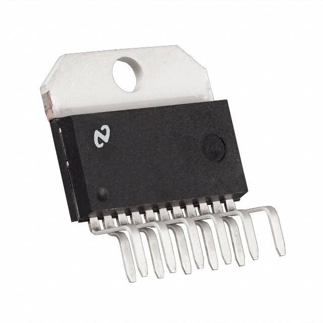
Connection Diagram
Figure 2. Top View
See Package Number NDJ0011B
2
Submit Documentation Feedback
Copyright © 1998–2013, Texas Instruments Incorporated
Product Folder Links: LMD18201
�LMD18201
www.ti.com
SNVS092D – APRIL 1998 – REVISED APRIL 2013
These devices have limited built-in ESD protection. The leads should be shorted together or the device placed in conductive foam
during storage or handling to prevent electrostatic damage to the MOS gates.
Absolute Maximum Ratings (1) (2)
Total Supply Voltage (VS, Pin 6)
60V
Voltage at Pins 3, 4, 5 and 9
12V
Voltage at Bootstrap Pins (Pins 1 and 11)
VOUT + 16V
Peak Output Current (200 ms)
Continuous Output Current
Power Dissipation
6A
(3)
3A
(4)
25W
+0.5V to −1.0V
Sense Voltage (Pin 7 to Pin 8)
Power Dissipation (TA = 25°C, Free Air)
3W
Junction Temperature, TJ(max)
ESD Susceptibility
150°C
(5)
1500V
−40°C to +150°C
Storage Temperature, TSTG
Lead Temperature (Soldering, 10 sec.)
(1)
300°C
Absolute Maximum Ratings indicate limits beyond which damage to the device may occur. DC and AC electrical specifications do not
apply when operating the device beyond its rated operating conditions.
If Military/Aerospace specified devices are required, please contact the Texas Instruments Sales Office/Distributors for availability and
specifications.
See Application Information for details regarding current limiting.
The maximum power dissipation must be derated at elevated temperatures and is a function of TJ(max), θJA, and TA. The maximum
allowable power dissipation at any temperature is PD(max) = (TJ(max) − TA)/θJA, or the number given in the Absolute Ratings, whichever is
lower. The typical thermal resistance from junction to case (θJC) is 1.0°C/W and from junction to ambient (θJA) is 30°C/W. For ensured
operation TJ(max) = 125°C.
Human-body model, 100 pF discharged through a 1.5 kΩ resistor. Except Bootstrap pins (pins 1 and 11) which are protected to 1000V
of ESD.
(2)
(3)
(4)
(5)
Operating Ratings (1)
−40°C to +125°C
Junction Temperature, TJ
VS Supply Voltage
(1)
+12V to +55V
Absolute Maximum Ratings indicate limits beyond which damage to the device may occur. DC and AC electrical specifications do not
apply when operating the device beyond its rated operating conditions.
Electrical Characteristics (1)
The following specifications apply for VS = 42V, unless otherwise specified. Boldface limits apply over the entire operating
temperature range, −40°C ≤ TJ ≤ +125°C, all other limits are for TA = TJ = 25°C.
Symbol
Parameter
Conditions
Typ
Limit
Units
(2)
0.33
0.40/0.6
Ω (max)
Output Current = 6A
(2)
0.38
0.45/0.6
Ω (max)
(2)
1.2
1.5
V (max)
RDS(ON)
Switch ON Resistance
Output Current = 3A
RDS(ON)
Switch ON Resistance
VCLAMP
Clamp Diode Forward Drop
Clamp Current = 3A
VIL
Logic Low Input Voltage
Pins 3, 4, 5
IIL
Logic Low Input Current
VIN = −0.1V, Pins = 3, 4, 5
VIH
Logic High Input Voltage
Pins 3, 4, 5
IIL
−0.1
V (min)
0.8
V (max)
−10
μA (max)
2
V (min)
12
V (max)
μA (max)
Logic High Input Current
VIN = 12V, Pins = 3, 4, 5
10
Undervoltage Lockout
Outputs Turn OFF
9
V (min)
11
V (max)
TJW
Warning Flag Temperature
Pin 9 ≤ 0.8V, IL = 2 mA
145
°C
VF(ON)
Flag Output Saturation Voltage
TJ = TJW, IL = 2 mA
0.15
V
(1)
(2)
All limits are 100% production tested at 25°C. Temperature extreme limits are ensured via correlation using accepted SQC (Statistical
Quality Control) methods. All limits are used to calculate AOQL, (Average Outgoing Quality Level).
Output currents are pulsed (tW < 2 ms, Duty Cycle < 5%).
Submit Documentation Feedback
Copyright © 1998–2013, Texas Instruments Incorporated
Product Folder Links: LMD18201
3
�LMD18201
SNVS092D – APRIL 1998 – REVISED APRIL 2013
www.ti.com
Electrical Characteristics(1) (continued)
The following specifications apply for VS = 42V, unless otherwise specified. Boldface limits apply over the entire operating
temperature range, −40°C ≤ TJ ≤ +125°C, all other limits are for TA = TJ = 25°C.
Typ
Limit
Units
IF(OFF)
Symbol
Flag Output Leakage
VF = 12V
0.2
10
μA (max)
TJSD
Shutdown Temperature
Outputs Turn OFF
170
IS
Quiescent Supply Current
All Logic Inputs Low
13
25
mA (max)
tD(ON)
Output Turn-On Delay Time
Sourcing Outputs, IOUT = 3A
300
ns
Sinking Outputs, IOUT = 3A
300
ns
Sourcing Outputs, IOUT = 3A
100
ns
Sinking Outputs, IOUT = 3A
80
ns
Sourcing Outputs, IOUT = 3A
200
ns
Sinking Outputs, IOUT = 3A
200
ns
Sourcing Outputs, IOUT = 3A
75
ns
Sinking Outputs, IOUT = 3A
70
ns
tON
tD(OFF)
tOFF
Parameter
Output Turn-On Switching Time
Output Turn-Off Delay Times
Output Turn-Off Switching Times
Conditions
°C
Bootstrap Capacitor = 10 nF
Bootstrap Capacitor = 10 nF
tPW
Minimum Input Pulse Width
Pins 3, 4 and 5
1
μs
tCPR
Charge Pump Rise Time
No Bootstrap Capacitor
20
μs
4
Submit Documentation Feedback
Copyright © 1998–2013, Texas Instruments Incorporated
Product Folder Links: LMD18201
�LMD18201
www.ti.com
SNVS092D – APRIL 1998 – REVISED APRIL 2013
Typical Performance Characteristics
VSAT vs Flag Current
RDS(ON) vs Temperature
Figure 3.
Figure 4.
RDS(ON) vs Supply Voltage
Supply Current vs Supply Voltage
Figure 5.
Figure 6.
Supply Current vs Frequency (VS = 42V)
Supply Current vs Temperature (VS = 42V)
Figure 7.
Figure 8.
Submit Documentation Feedback
Copyright © 1998–2013, Texas Instruments Incorporated
Product Folder Links: LMD18201
5
�LMD18201
SNVS092D – APRIL 1998 – REVISED APRIL 2013
www.ti.com
TEST CIRCUIT
Switching Time Definitions
6
Submit Documentation Feedback
Copyright © 1998–2013, Texas Instruments Incorporated
Product Folder Links: LMD18201
�LMD18201
www.ti.com
SNVS092D – APRIL 1998 – REVISED APRIL 2013
Pinout Descriptions
(See Test Circuit)
Pin 1, BOOTSTRAP 1 Input: Bootstrap capacitor pin for half H-Bridge number 1. The recommended capacitor
(10 nF) is connected between pins 1 and 2.
Pin 2, OUTPUT 1: Half H-Bridge number 1 output.
Pin 3, DIRECTION Input: See Logic Truth Table. This input controls the direction of current flow between
OUTPUT 1 and OUTPUT 2 (pins 2 and 10) and, therefore, the direction of rotation of a motor load.
Pin 4, BRAKE Input: See Logic Truth Table. This input is used to brake a motor by effectively shorting its
terminals. When braking is desired, this input is taken to a logic high level and it is also necessary to apply logic
high to PWM input, pin 5. The drivers that short the motor are determined by the logic level at the DIRECTION
input (Pin 3): with Pin 3 logic high, both current sourcing output transistors are ON; with Pin 3 logic low, both
current sinking output transistors are ON. All output transistors can be turned OFF by applying a logic high to Pin
4 and a logic low to PWM input Pin 5; in this case only a small bias current (approximately −1.5 mA) exists at
each output pin.
Pin 5, PWM Input: See Logic Truth Table. How this input (and DIRECTION input, Pin 3) is used is determined
by the format of the PWM Signal.
Pin 6, VS Power Supply
Pin 7, POWER GROUND/SENSE Connection: This pin is the ground return for the power DMOS transistors of
the H-Bridge. The current through the H-Bridge can be sensed by adding a small, 0.1Ω, sense resistor from this
pin to the power supply ground.
Pin 8, SIGNAL GROUND: This is the ground return for the internal logic circuitry used to control the PWM
switching of the H-Bridge.
Pin 9, THERMAL FLAG Output: This pin provides the thermal warning flag output signal. Pin 9 becomes activelow at 145°C (junction temperature). However the chip will not shut itself down until 170°C is reached at the
junction.
Pin 10, OUTPUT 2: Half H-Bridge number 2 output.
Pin 11, BOOTSTRAP 2 Input: Bootstrap capacitor pin for half H-Bridge number 2. The recommended capacitor
(10 nF) is connected between pins 10 and 11.
Logic Truth Table
PWM
Dir
Brake
H
H
L
Source 1, Sink 2
Active Output Drivers
H
L
L
Sink 1, Source 2
L
X
L
Source 1, Source 2
H
H
H
Source 1, Source 2
H
L
H
Sink 1, Sink 2
L
X
H
NONE
Submit Documentation Feedback
Copyright © 1998–2013, Texas Instruments Incorporated
Product Folder Links: LMD18201
7
�LMD18201
SNVS092D – APRIL 1998 – REVISED APRIL 2013
www.ti.com
APPLICATION INFORMATION
TYPES OF PWM SIGNALS
The LMD18201 readily interfaces with different forms of PWM signals. Use of the part with two of the more
popular forms of PWM is described in the following paragraphs.
Simple, locked anti-phase PWM consists of a single, variable duty-cycle signal in which is encoded both
direction and amplitude information (see Figure 9). A 50% duty-cycle PWM signal represents zero drive, since
the net value of voltage (integrated over one period) delivered to the load is zero. For the LMD18201, the PWM
signal drives the direction input (pin 3) and the PWM input (pin 5) is tied to logic high.
Figure 9. Locked Anti-Phase PWM Control
Sign/magnitude PWM consists of separate direction (sign) and amplitude (magnitude) signals (see Figure 10).
The (absolute) magnitude signal is duty-cycle modulated, and the absence of a pulse signal (a continuous logic
low level) represents zero drive. Current delivered to the load is proportional to pulse width. For the LMD18201,
the DIRECTION input (pin 3) is driven by the sign signal and the PWM input (pin 5) is driven by the magnitude
signal.
Figure 10. Sign/Magnitude PWM Control
8
Submit Documentation Feedback
Copyright © 1998–2013, Texas Instruments Incorporated
Product Folder Links: LMD18201
�LMD18201
www.ti.com
SNVS092D – APRIL 1998 – REVISED APRIL 2013
Figure 11. Transitions in Brake, Direction, or PWM Must be Separated by At Least 1 μsec
SIGNAL TRANSITION REQUIREMENTS
To ensure proper internal logic performance, it is good practice to avoid aligning the falling and rising edges of
input signals. A delay of at least 1 µsec should be incorporated between transitions of the Direction, Brake,
and/or PWM input signals. A conservative approach is be sure there is at least 500ns delay between the end of
the first transition and the beginning of the second transition. See Figure 11.
USING THE THERMAL WARNING FLAG
The THERMAL FLAG output (pin 9) is an open collector transistor. This permits a wired OR connection of
thermal warning flag outputs from multiple LMD18201's, and allows the user to set the logic high level of the
output signal swing to match system requirements. This output typically drives the interrupt input of a system
controller. The interrupt service routine would then be designed to take appropriate steps, such as reducing load
currents or initiating an orderly system shutdown. The maximum voltage compliance on the flag pin is 12V.
SUPPLY BYPASSING
During switching transitions the levels of fast current changes experienced may cause troublesome voltage
transients across system stray inductances.
It is normally necessary to bypass the supply rail with a high quality capacitor(s) connected as close as possible
to the VS Power Supply (Pin 6) and POWER GROUND (Pin 7). A 1 μF high-frequency ceramic capacitor is
recommended. Care should be taken to limit the transients on the supply pin below the Absolute Maximum
Rating of the device. When operating the chip at supply voltages above 40V a voltage suppressor (transorb)
such as P6KE62A is recommended from supply to ground. Typically the ceramic capacitor can be eliminated in
the presence of the voltage suppressor. Note that when driving high load currents a greater amount of supply
bypass capacitance (in general at least 100 μF per Amp of load current) is required to absorb the recirculating
currents of the inductive loads.
Submit Documentation Feedback
Copyright © 1998–2013, Texas Instruments Incorporated
Product Folder Links: LMD18201
9
�LMD18201
SNVS092D – APRIL 1998 – REVISED APRIL 2013
www.ti.com
CURRENT LIMITING
Current limiting protection circuitry has been incorporated into the design of the LMD18201. With any power
device it is important to consider the effects of the substantial surge currents through the device that may occur
as a result of shorted loads. The protection circuitry monitors the current through the upper transistors and shuts
off the power device as quickly as possible in the event of an overload condition (the threshold is set to
approximately 10A). In a typical motor driving application the most common overload faults are caused by
shorted motor windings and locked rotors. Under these conditions the inductance of the motor (as well as any
series inductance in the VCC supply line) serves to reduce the magnitude of a current surge to a safe level for the
LMD18201. Once the device is shut down, the control circuitry will periodically try to turn the power device back
on. This feature allows the immediate return to normal operation once the fault condition has been removed.
While the fault remains however, the device will cycle in and out of thermal shutdown. This can create voltage
transients on the VCC supply line and therefore proper supply bypassing techniques are required.
The most severe condition for any power device is a direct, hard-wired (“screwdriver”) long term short from an
output to ground. This condition can generate a surge of current through the power device on the order of 15
Amps and require the die and package to dissipate up to 500W of power for the short time required for the
protection circuitry to shut off the power device. This energy can be destructive, particularly at higher operating
voltages (>30V) so some precautions are in order. Proper heat sink design is essential and it is normally
necessary to heat sink the VCC supply pin (pin 6) with 1 square inch of copper on the PC board.
INTERNAL CHARGE PUMP AND USE OF
BOOTSTRAP CAPACITORS
To turn on the high-side (sourcing) DMOS power devices, the gate of each device must be driven approximately
8V more positive than the supply voltage. To achieve this an internal charge pump is used to provide the gate
drive voltage. As shown in (Figure 12), an internal capacitor is alternately switched to ground and charged to
about 14V, then switched to VS thereby providing a gate drive voltage greater than VS. This switching action is
controlled by a continuously running internal 300 kHz oscillator. The rise time of this drive voltage is typically 20
μs which is suitable for operating frequencies up to 1 kHz.
Figure 12. Internal Charge Pump Circuitry
For higher switching frequencies, the LMD18201 provides for the use of external bootstrap capacitors. The
bootstrap principle is in essence a second charge pump whereby a large value capacitor is used which has
enough energy to quickly charge the parasitic gate input capacitance of the power device resulting in much faster
rise times. The switching action is accomplished by the power switches themselves (Figure 13). External 10 nF
capacitors, connected from the outputs to the bootstrap pins of each high-side switch provide typically less than
100 ns rise times allowing switching frequencies up to 500 kHz.
10
Submit Documentation Feedback
Copyright © 1998–2013, Texas Instruments Incorporated
Product Folder Links: LMD18201
�LMD18201
www.ti.com
SNVS092D – APRIL 1998 – REVISED APRIL 2013
Figure 13. Bootstrap Circuitry
INTERNAL PROTECTION DIODES
A major consideration when switching current through inductive loads is protection of the switching power
devices from the large voltage transients that occur. Each of the four switches in the LMD18201 have a built-in
protection diode to clamp transient voltages exceeding the positive supply or ground to a safe diode voltage drop
across the switch.
The reverse recovery characteristics of these diodes, once the transient has subsided, is important. These
diodes must come out of conduction quickly and the power switches must be able to conduct the additional
reverse recovery current of the diodes. The reverse recovery time of the diodes protecting the sourcing power
devices is typically only 70 ns with a reverse recovery current of 1A when tested with a full 3A of forward current
through the diode. For the sinking devices the recovery time is typically 100 ns with 4A of reverse current under
the same conditions.
TYPICAL APPLICATIONS
BASIC MOTOR DRIVER
The LMD18201 can directly interface to any Sign/Magnitude PWM controller. The LM629 is a motion control
processor that outputs a Sign/Magnitude PWM signal to coordinate either positional or velocity control of DC
motors. The LMD18201 provides fully protected motor driver stage.
Figure 14. Basic Motor Driver
Submit Documentation Feedback
Copyright © 1998–2013, Texas Instruments Incorporated
Product Folder Links: LMD18201
11
�LMD18201
SNVS092D – APRIL 1998 – REVISED APRIL 2013
www.ti.com
CURRENT SENSING
In many motor control applications it is desirable to sense and control the current through the motor. For these
types of applications a companion product, the LMD18200, is also available. The LMD18200 is identical to the
LMD18201 but has current sensing transistors that output a current directly proportional to the current conducted
by the two upper DMOS power devices to a separate current sense pin. This technique does not require a low
valued, power sense resistor and does not subtract from the available voltage drive to the motor.
To sense the bridge current through the LMD18201 requires the addition of a small sense resistor between the
power ground/sense pin (Pin 7) and the actual circuit ground (see Figure 15). This resistor should have a value
of 0.1Ω or less to stay within the allowable voltage compliance of the sense pin, particularly at higher operating
current levels. The voltage between power ground/sense (Pin 7) and the signal ground (Pin 8) must stay within
the range of −1V to +0.5V. Internally there is approximately 25Ω between pins 7 and 8 and this resistance will
slightly reduce the value of the external sense resistor. Approximately 70% of the quiescent supply current (10
mA) flows out of pin 7. This will cause a slight offset to the voltage across the sense resistor when the bridge is
not conducting. During reverse recovery of the internal protection diodes the voltage compliance between pins 7
and 8 may be exceeded. The duration of these spikes however are only approximately 100 ns and do not have
enough time or energy to disrupt the operation of the LMD18201.
Figure 15. Current Sensing
12
Submit Documentation Feedback
Copyright © 1998–2013, Texas Instruments Incorporated
Product Folder Links: LMD18201
�LMD18201
www.ti.com
SNVS092D – APRIL 1998 – REVISED APRIL 2013
REVISION HISTORY
Changes from Revision C (April 2013) to Revision D
•
Page
Changed layout of National Data Sheet to TI format .......................................................................................................... 12
Submit Documentation Feedback
Copyright © 1998–2013, Texas Instruments Incorporated
Product Folder Links: LMD18201
13
�PACKAGE OPTION ADDENDUM
www.ti.com
30-Sep-2021
PACKAGING INFORMATION
Orderable Device
Status
(1)
Package Type Package Pins Package
Drawing
Qty
Eco Plan
(2)
Lead finish/
Ball material
MSL Peak Temp
Op Temp (°C)
(3)
Device Marking
(4/5)
(6)
LMD18201T
NRND
TO-220
NDJ
11
20
Non-RoHS
& Green
Call TI
Level-1-NA-UNLIM
-40 to 125
LMD18201T P+
LMD18201T/NOPB
ACTIVE
TO-220
NDJ
11
20
RoHS & Green
SN
Level-1-NA-UNLIM
-40 to 125
LMD18201T P+
(1)
The marketing status values are defined as follows:
ACTIVE: Product device recommended for new designs.
LIFEBUY: TI has announced that the device will be discontinued, and a lifetime-buy period is in effect.
NRND: Not recommended for new designs. Device is in production to support existing customers, but TI does not recommend using this part in a new design.
PREVIEW: Device has been announced but is not in production. Samples may or may not be available.
OBSOLETE: TI has discontinued the production of the device.
(2)
RoHS: TI defines "RoHS" to mean semiconductor products that are compliant with the current EU RoHS requirements for all 10 RoHS substances, including the requirement that RoHS substance
do not exceed 0.1% by weight in homogeneous materials. Where designed to be soldered at high temperatures, "RoHS" products are suitable for use in specified lead-free processes. TI may
reference these types of products as "Pb-Free".
RoHS Exempt: TI defines "RoHS Exempt" to mean products that contain lead but are compliant with EU RoHS pursuant to a specific EU RoHS exemption.
Green: TI defines "Green" to mean the content of Chlorine (Cl) and Bromine (Br) based flame retardants meet JS709B low halogen requirements of