LMH0041, LMH0051
LMH0071, LMH0341
www.ti.com
SNLS272Q – APRIL 2007 – REVISED APRIL 2013
3 Gbps, HD, SD, DVB-ASI SDI Deserializer with Loopthrough and LVDS Interface
Check for Samples: LMH0041, LMH0051, LMH0071, LMH0341
FEATURES
DESCRIPTION
•
•
•
The LMH0341/0041/0071/0051 SDI Deserializers are
part of TI’s family of FPGA-Attach SER/DES products
supporting 5-bit LVDS interfaces with FPGAs. When
paired with a host FPGA the LMH0341 automatically
detects the incoming data rate and decodes the raw
5-bit data words compliant to any of the following
standards: DVB-ASI, SMPTE 259M, SMPTE 292M,
or SMPTE 424M. See Table 1 for details on which
Standards are supported per device.
1
23
•
•
•
•
5-Bit LVDS Interface
No External VCO or Clock Required
Reclocked Serial Loopthrough With Cable
Driver
Powerdown Mode
3.3V SMBus Configuration Interface
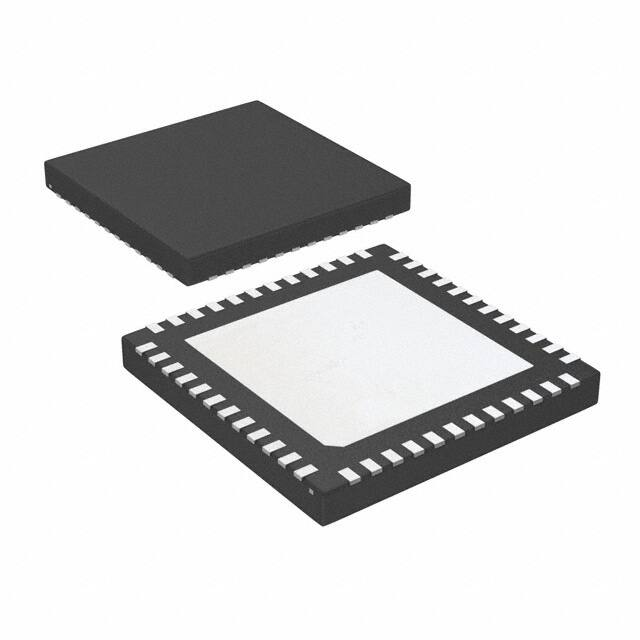
Small 48-Pin WQFN Package
Industrial Temperature range: -40°C to +85°C
APPLICATIONS
•
SDI Interfaces for:
– Video Cameras
– DVRs
– Video Switchers
– Video Editing Systems
KEY SPECIFICATIONS
•
•
•
Output compliant with SMPTE 259M-C, SMPTE
292M, SMPTE 424M and DVB-ASI (See Table 1)
Typical power dissipation: 590 mW
(loopthrough disabled, 3G datarate)
0.6 UI Minimum Input Jitter Tolerance
The interface between the LMH0341 and the host
FPGA consists of a 5-bit wide LVDS bus, an LVDS
clock and an SMBus interface. No external VCOs or
clocks are required. The LMH0341 CDR detects the
frequency from the incoming data stream, generates
a clean clock and transmits both clock and data to
the host FPGA. The LMH0341, LMH0041 and
LMH0071 include a serial reclocked loopthrough with
integrated SMPTE compliant cable driver. Refer to
Table 1 for a complete listing of single channel
deserializers offered in this family.
The FPGA-Attach SER/DES product family is
supported by a suite of IP which allows the design
engineer to quickly develop video applications using
the SER/DES products. The product is packaged in a
physically small 48 pin WQFN package.
General Block Diagram
RESET
LOCK
GPIO[2:0]
DVB_ASI
Loopthru_EN
Control
SDA
SCK
SMB_CS
SMBus
RXCLK
CLK
MUX
CDR
RXIN1
Data
RX4
Bypassable 8b10b Decode
RXIN0
Serial to Parallel 1:5
RX_MUX_SEL
RX3
RX2
RX1
TXOUT
RX0
LVDS Drivers
SMPTE Cable Driver
1
2
3
Please be aware that an important notice concerning availability, standard warranty, and use in critical applications of
Texas Instruments semiconductor products and disclaimers thereto appears at the end of this data sheet.
TRI-STATE is a registered trademark of National Semiconductor Corporation.
All other trademarks are the property of their respective owners.
PRODUCTION DATA information is current as of publication date.
Products conform to specifications per the terms of the Texas
Instruments standard warranty. Production processing does not
necessarily include testing of all parameters.
Copyright © 2007–2013, Texas Instruments Incorporated
�LMH0041, LMH0051
LMH0071, LMH0341
SNLS272Q – APRIL 2007 – REVISED APRIL 2013
www.ti.com
RX4-
RX4+
RX3-
RX3+
RX2-
RX2+
RX1-
RX1+
RX0-
RX0+
RXCLK-
RXCLK+
Connection Diagrams
48
47
46
45
44
43
42
41
40
39
38
37
VDD3V3
1
36
VDD3V3
Loopthru_EN
2
35
VDD2V5
GPIO_0
3
34
SMB_CS
GPIO_1
4
33
SCK
32
SDA
31
LOCK
30
RESET
29
GND
28
VDDPLL
LMH0341,
LMH0041,
LMH0071
RSVD_H
5
DVB_ASI
6
VDD2V5
7
GND
8
GND
9
GND
10
27
LF_CP
GPIO_2
11
26
LF_REF
RX_MUX_SEL
12
25
VDD2V5
TOP VIEW
(not to scale)
48-pin WQFN Package
17
18
19
20
RSET
VDD3V3
RXIN0+
RXIN0-
VDD3V3
RXIN1+
RXIN1-
21
22
23
24
GND
16
GND
15
TXOUT-
14
TXOUT+
13
DNC
DAP = GND
Figure 1. Connection Diagram for LMH0341 / LMH0041 / LMH0071
2
Submit Documentation Feedback
Copyright © 2007–2013, Texas Instruments Incorporated
Product Folder Links: LMH0041 LMH0051 LMH0071 LMH0341
�LMH0041, LMH0051
LMH0071, LMH0341
RX4+
RX3-
RX3+
RX2-
RX2+
RX1-
RX1+
RX0-
RX0+
RXCLK-
RXCLK+
SNLS272Q – APRIL 2007 – REVISED APRIL 2013
RX4-
www.ti.com
48
47
46
45
44
43
42
41
40
39
38
37
VDD3V3
1
36
VDD3V3
N/C
2
35
VDD2V5
GPIO_0
3
34
SMB_CS
GPIO_1
4
33
SCK
RSVD_H
5
32
SDA
DVB_ASI
6
31
LOCK
VDD2V5
7
30
RESET
GND
8
29
GND
GND
9
28
VDDPLL
GND
10
27
LF_CP
GPIO2
11
26
LF_REF
RX_MUX_SEL
12
25
VDD2V5
LMH0051
TOP VIEW
(not to scale)
48-pin WQFN Package
DNC
22
23
24
GND
21
GND
20
DNC
19
RXIN1-
18
RXIN1+
17
VDD3V3
16
RXIN0-
RSET
15
RXIN0+
14
VDD3V3
13
GND
DAP = GND
Figure 2. Connection Diagram for LMH0051
Copyright © 2007–2013, Texas Instruments Incorporated
Submit Documentation Feedback
Product Folder Links: LMH0041 LMH0051 LMH0071 LMH0341
3
�LMH0041, LMH0051
LMH0071, LMH0341
SNLS272Q – APRIL 2007 – REVISED APRIL 2013
www.ti.com
PIN DESCRIPTIONS
Pin Name
Type
Description
RX[4:0]+
RX[4:0]-
Output, LVDS
LVDS Data Output Pins
Five channel wide DDR interface.
RXCLK+
RXCLK-
Output, LVDS
LVDS Clock Output Pins
DDR Interface.
RXIN0+
RXIN0-
Input, Differential
Serial differential input Pins
Channel 0
RXIN1+
RXIN1-
Input, Differential
Serial differential input Pins
Channel 1
LVDS Input Interface
Serial Data Inputs
Loopthrough Serial Output
TXOUT+
Output, CML
Serial Digital Interface Output Pin
Non-Inverting Output
TXOUT-
Output, CML
Serial Digital Interface Output Pin
Inverting Output
SDA
I/O, LVCMOS
SMBus Data I/O Pin
SCK
Input, LVCMOS
SMBus Clock Input Pin
SMB_CS
Input, LVCMOS
SMBus Chip Select Input Pin
Device is selected when High.
SMBus Interface
Control and Configuration Pins
RESET
Input, LVCMOS
Reset Input Pin
H = normal mode
L = device in RESET
LOCK
Output, LVCMOS
PLL LOCK Status Output
H = unlock condition
L = PLL is Locked
DVB_ASI
Input, LVCMOS
DVB_ASI Select Input
H = DVB_ASI Mode enabled
L = Normal Mode enabled
Loopthru_EN
Input, LVCMOS
Loopthrough enable Input
H=Reclocked Loopthrogh active
L=Reclocked Loopthrough disabled
RX_MUX_SEL
Input, LVCMOS
Input multiplexer select
H=RXIN1 selected
L=RXIN0selected
GPIO[2:0]
I/O, LVCMOS
General Purpose Input / Output
Software configurable I/O pins.
RSVD_H
Input, LVCMOS
Configuration Input – Must tie High
Pull High via 5 kΩ resistor to VDD3V3
RSET
Input
Serial Loopthrough Output Amplitude Control
Resistor connected from this pin to ground to set the signal amplitude. Nominally 7.87kΩ
for 800mV output (SMPTE).
LF_CP
Input
Loop Filter Connection
Analog Inputs
LF_REF
Loop Filter Reference
DNC
Do Not Connect – Leave Open
Power Supply and Ground
VDD3V3
Power
3.3V Power Supply connection
VDDPLL
Power
3.3V PLL Power Supply connection
VDD2V5
Power
2.5V Power Supply connection
GND
Ground
Ground connection – The DAP (large center pad) is the primary GND connection for the
device and must be connected to Ground along with the GND pins.
4
Submit Documentation Feedback
Copyright © 2007–2013, Texas Instruments Incorporated
Product Folder Links: LMH0041 LMH0051 LMH0071 LMH0341
�LMH0041, LMH0051
LMH0071, LMH0341
www.ti.com
SNLS272Q – APRIL 2007 – REVISED APRIL 2013
Table 1. Feature Table
Device
LMH0341
SMPTE 424M
Support
SMPTE 292M
Support
SMPTE 259M
Support
DVB-ASI Support
Active Loopthrough
×
×
×
×
×
×
×
×
×
×
×
×
×
×
LMH0041
LMH0071
LMH0051
×
Copyright © 2007–2013, Texas Instruments Incorporated
Submit Documentation Feedback
Product Folder Links: LMH0041 LMH0051 LMH0071 LMH0341
5
�LMH0041, LMH0051
LMH0071, LMH0341
SNLS272Q – APRIL 2007 – REVISED APRIL 2013
www.ti.com
These devices have limited built-in ESD protection. The leads should be shorted together or the device placed in conductive foam
during storage or handling to prevent electrostatic damage to the MOS gates.
Absolute Maximum Ratings
(1) (2)
−0.3V to +4.0V
Supply Voltage (VDD3V3)
Supply Voltage(VDD2V5)
–0.3V to +3.0V
LVCMOS input voltage
−0.3V to (VDD3V3+0.3V)
LVCMOS output voltage
−0.3V to (VDD3V3+0.3V)
SMBus I/O Voltage
–0.3V to +3.6V
LVDS Input Voltage
0.3V to 3.6V
Junction Temperature
+150°C
Storage Temperature
−65° to 150°C
Lead Temperature—Soldering 4 seconds
+260°C
Thermal Resistance—
26°C/W
Junction to Ambient—θJA
ESD Rating—Human Body Model,
(1)
(2)
≥±8KV
1.5 KΩ, 100 pF
“Absolute Maximum Ratings” are the ratings beyond which the safety of the device cannot be ensured. It is not implied that the device
will operate up to these limits.
If Military/Aerospace specified devices are required, please contact the TI Sales Office/Distributors for availability and specifications.
Recommended Operating Conditions
Min
Typ
Max
Units
Supply Voltage (VDD3V3-GND)
Parameter
3.135
3.3
3.465
V
Supply Voltage (VDD2V5-GND)
2.375
2.5
2.625
V
100
mVP-P
+85
°C
Supply noise amplitude (10 Hz to 50 MHz)
−40
Ambient Temperature
+25
Case Temperature
Input Data Rate
270
2970
Mbps
LMH0041
270
1485
Mbps
LMH0071
270
270
Mbps
LMH0051
270
1485
Mbps
25
cm
RSTERM — SMBus termination resistor value
Ω
1000
Loopthrough Output Driver Pullup Resistor Termination Voltage (1)
6
°C
LMH0341
LVDS PCB board trace length (mismatch 12dB to
3 GHz
dB
Typical Parameters measured at VDD=3.3V, TA=25°C. They are for reference purposes and are not production tested.
Specification ensured by characterization
LVDS Output Electrical Characteristics
Over supply and Operating Temperature ranges unless otherwise specified.
Symbol
Parameter
VOD
Differential Output Voltage
ΔVOD
Change in VOD between
complementary output states
VOS
Offset Voltage
ΔVOS
Change in VOS between
complementary output states
IOS
Output Short Circuit Current
(1)
8
Condition
RL = 100Ω
(1)
Min
230
1.125
VOUT = 0V, RL = 100Ω
Typ
1.25
Max
Units
310
mV
35
mV
1.375
V
35
mV
—50
mA
Typical Parameters measured at VDD=3.3V, TA=25°C. They are for reference purposes and are not production tested.
Submit Documentation Feedback
Copyright © 2007–2013, Texas Instruments Incorporated
Product Folder Links: LMH0041 LMH0051 LMH0071 LMH0341
�LMH0041, LMH0051
LMH0071, LMH0341
www.ti.com
SNLS272Q – APRIL 2007 – REVISED APRIL 2013
LVDS Switching Characteristics
Over supply and Operating Temperature ranges unless otherwise specified.
Symbol
Parameter
(1)
Condition
Min
tROTR
LVDS Low to High Transition time
tROTF
LVDS High to Low Transition time
tROCP
Receiver output clock period
tRODC
RxCLKOUT Duty Cycle
tROCH
RxCLKOUT high time
tROCL
RxCLKOUT low time
tRBIT
Receiver output bit width
tDVBC
tDVAC
RX data transition to RXCLK transition See Receiver timing
specifications (2)
RXCLK transition to RX data transition
tROJR
Receiver output Random Jitter
tROJT
Peak-to-Peak Receiver Output Jitter
tRD
Receiver Propagation Delay
See Figure 5 Receiver (LVDS
Interface) Propagation Delay
tRLA
Receiver Link Acquisition Time
From device reset or change in
input data rate to locked
condition
tLVSK
LVDS Output Skew
LVDS Differential Output Skew
between + and − pins
(1)
(2)
(3)
Typ
Max
Units
See Figure 3 LVDS Switching
times
300
ps
300
ps
RxCLKOUT is DDR. If divide by
4 is enabled, the output clock
period will be doubled
2T
ns
45
See Receiver timing
specifications
50
55
1.51
%
ns
1.51
ns
T
ns
650
ps
650
ps
Receiver output intrinsic random
jitter. Bit error rate ≤ 10-15.
Alternating 10 pattern. RMS (3)
2.5
(3)
ps
70
125
ps
24
ms
12 T
20
ps
Typical Parameters measured at VDD=3.3V, TA=25°C. They are for reference purposes and are not production tested.
Specification Characterized at 2.97 Gbps, 1.485 Gbps and 270 Mbps, production tested at 270 Mbps only
Specification ensured by characterization
t ROCL
tROCH
80%
80%
RXCLKOUT
20%
20%
tROTR
tROTF
RX[4:0]
t DVBC
t DVBC
t DVAC
t DVAC
Figure 3. LVDS Switching Times
Copyright © 2007–2013, Texas Instruments Incorporated
Submit Documentation Feedback
Product Folder Links: LMH0041 LMH0051 LMH0071 LMH0341
9
�LMH0041, LMH0051
LMH0071, LMH0341
SNLS272Q – APRIL 2007 – REVISED APRIL 2013
www.ti.com
SMBus Input Electrical Characteristics
Over supply and Operating Temperature ranges unless otherwise specified.
Symbol
Parameter
Condition
VSIL
Data, Clock Input Low Voltage
VSIH
Data, Clock Input High Voltage
VSDD
Nominal Bus Voltage
VOL
Output Low voltage
Min
Typ
(2)
Input Leakage per bus segment
See
ISLEAKP
Input Leakage per pin
SCK and SDA pins
CSI
Capacitance for SMBdata and SMBclk See
Max
Units
0.8
V
2.1
VSDD
V
2.375
3.465
V
0.3
V
−200
200
μA
−10
10
μA
10
pF
IOL=2mA
ISLEAKB
(1)
(2)
(3)
(1)
(2) (3)
Typical Parameters measured at VDD=3.3V, TA=25°C. They are for reference purposes and are not production tested.
Recommended value—Parameter is not tested.
Recommended maximum capacitance load per bus segment is 400 pF.
SMBus Switching Characteristics
Over supply and Operating Temperature ranges unless otherwise specified.
Symbol
Parameter
(1)
Condition
Min
Typ
Max
Units
100
kHz
fSMB
Bus Operating Frequency
10
tBUF
Bus free time between stop and start
condition
4.7
μs
tSU:CS
Minimum time between SMB_CS
being active and Start condition
(2)
30
ns
tH:CS
Minimum time between stop condition
and releasing SMB_CS
(2)
100
ns
tHD:STA
Hold time after (repeated) start
condition. After this period, the first
clock is generated
4.0
μs
tSU:STA
Repeated Start condition setup time
4.7
μs
tSU:STO
Stop Condition setup time
4.0
μs
tHD:DAT
Data hold time
300
ns
tSU:DAT
Data setup time
250
ns
tLOW
Clock Low Period
4.7
μs
tHIGH
Clock high time
4.0
tPOR
Time in which a device must be
operational after power on
(1)
(2)
At ISPULLUP = MAX
50
μs
500
ms
Typical Parameters measured at VDD=3.3V, TA=25°C. They are for reference purposes and are not production tested.
Specification ensured by characterization
tSU:CS
SMB_CS
tLOW
tR
tH:CS
tHIGH
SCK
tHD:STA
tBUF
tHD:DAT
tF
tSU:STA
tSU:DAT
tSU:STO
SDA
SP
ST
SP
ST
Figure 4. SMBus Timing Parameters
10
Submit Documentation Feedback
Copyright © 2007–2013, Texas Instruments Incorporated
Product Folder Links: LMH0041 LMH0051 LMH0071 LMH0341
�LMH0041, LMH0051
LMH0071, LMH0341
www.ti.com
SNLS272Q – APRIL 2007 – REVISED APRIL 2013
SDI Output Switching Characteristics (LMH0341 / LMH0041 / LMH0071)
Over supply and Operating Temperature ranges unless otherwise specified.
Symbol
Parameter
(1)
Condition
Min
SDI Output Datarate
tr
270
SDI Output Rise Time
SDI Output Fall Time
MHz
135
ps
DR=1.485 Gbps (2)
145
DR=2.97 Gbps
400
1000
(2)
DR = 270 Mbps (2)
Mismatch between Rise and Fall
times
tSD
Propagation Delay Latency
tJ
Peak to Peak Output Jitter
2.97 Gbps
400
ps
145
ps
1000
ps
25
ps
1.485 Gbps (2)
30
ps
270 Mbps (2)
100
ps
tCIP
2.97 Gbps (2)
270 Mbps (2)
(3)
ns
25
(3)
(3)
VOD
SDI Output Voltage(Loopthrough
Output)
Into 75Ω Load
RL
Output Return Loss
Measured 5 MHz to 1483 MHz (2)
(1)
(2)
(3)
135
(2)
1.485 Gbps (2)
tOS
Units
2970
DR=1.485 Gbps (2)
Δtt
Max
DR=2.97 Gbps (2)
DR=270 Mbps (2)
tf
Typ
720
40
35
50
65
110
800
880
15
dB
(2)
Output Overshoot
mV
5
%
Typical Parameters measured at VDD=3.3V, TA=25°C. They are for reference purposes and are not production tested.
Specification ensured by characterization
Measured in accordance with SMPTE RP184.
Symbol N-1
Symbol N+1
Symbol N
Symbol N+3
Symbol N+2
Symbol N+4
RXIN
tRD
RXCLK
RX[0..4]
Symbol N-4
Symbol N-3
Symbol N-2
Symbol N-1
Symbol N
T
Figure 5. Receiver (LVDS Interface) Propagation Delay
Copyright © 2007–2013, Texas Instruments Incorporated
Submit Documentation Feedback
Product Folder Links: LMH0041 LMH0051 LMH0071 LMH0341
11
�LMH0041, LMH0051
LMH0071, LMH0341
SNLS272Q – APRIL 2007 – REVISED APRIL 2013
www.ti.com
FUNCTIONAL DESCRIPTION
DEVICE OPERATION
The DES is used in digital video signal origination equipment. It is intended to be operated in conjunction with an
FPGA host which processes data received by the SER, and converts the five bit output data to an appropriate
parallel video format — usually 10 or 20 bits wide. In most applications, the input data to the DES will be data
compliant with DVB ASI, SMPTE 259M-C, SMPTE 292M or SMPTE 424M, and the decoding will be done by the
IP provided by TI or similar IP to result in a decoded output. TI offers IP in source code format to perform the
appropriate decoding of the data, as well as evaluation platforms to assist in the development of target
applications. For more information please contact your local TI Sales Office/Distributor
POWER SUPPLIES
The DES has several power supply pins, at 2.5V as well as 3.3V. It is important that these pins all be connected,
and properly bypassed. Bypassing should consist of parallel 4.7μF and 0.1μF capacitors as a minimum, with a
0.1μF capacitor on each power pin. The device has a large contact in the center of the bottom of the package.
This contact must be connected to the system GND as it is the major ground connection for the device. A 22 μF
capacitor is required on the VDDPLL pin which is connected to the 3.3V rail
Discrete bypassing is ineffective above 30 MHz to 50 MHz in power plane-based distribution systems. Above this
frequency range, the intrinsic capacitance of the power-ground system can be used to provide additional RF
bypassing. To make the best use of this, make certain that there are PCB layers dedicated to the Power supplies
and to GND, and that they are placed next to each other to provide a distributed capacitance between power and
GND.
The DES will work best when powered from linear regulators. The output of linear regulators is generally cleaner
with less noise than switching regulators. Output filtering and power system frequency compensation are
generally simpler and more effective with linear regulators. Low dropout linear regulators are available which can
usually operate from lower input voltages such as logic power supplies, thereby reducing regulator power
dissipation. Cascading of low dropout regulators should not be done since this places the entire supply current
load of both load systems on the first regulator in the cascade and increases its loading and thermal output.
POWER UP
The 3.3V power supply should be brought up before the 2.5V supply. The timing of the supply sequencing is not
important. The device has a power on reset sequence which takes place once both power supplies are brought
up. This sequence will reset all register contents to their default values, and will place the PLLs into link
acquisition mode, attempting to lock on the RXIN0input.
RESET
There are three ways in which the device may be reset. There is an automatic reset which happens on power-up;
there is a reset pin, which when brought low will reset the device, with normal operation resuming when the pin is
driven high again. The third way to reset the device is a soft reset, implemented via a write to the reset register.
This reset will put all of the register values back to their default values, except it will not affect the address
register value if the SMBus default address has been changed.
LVDS OUTPUTS
The DES has LVDS outputs, compatible with ANSI/TIA/EIA-644. LVDS outputs expect to drive a 100Ω
transmission line which is properly terminated at the host FPGA inputs. It is recommended that the PCB trace
between the FPGA and the receiver be less than 25 cm. Longer PCB traces may introduce signal degradation as
well as channel skew which could cause serialization errors.
The LVDS outputs on the DES have a programmable output swing. The default condition is for the smaller size
swing, in order to save power. If a larger amplitude output swing is desired, this can be effected through the use
of register 0x27h
12
Submit Documentation Feedback
Copyright © 2007–2013, Texas Instruments Incorporated
Product Folder Links: LMH0041 LMH0051 LMH0071 LMH0341
�LMH0041, LMH0051
LMH0071, LMH0341
www.ti.com
SNLS272Q – APRIL 2007 – REVISED APRIL 2013
LVDS OUTPUT TIMING
The DES output timing, in it's default condition, is described in LVDS Switching Characteristics. The user has the
ability to adjust the LVDS output timing to make it easier to latch into the host FPGA if desired. This is done via
register 0x28h where both the clock to data timing may be adjusted, as well as changing the RXCLK from being
a DDR clock to a clock at the rate of DDR/2
LOOP FILTER
The DES has an internal PLL which is used to recover the embedded clock from the input data. The loop filter for
this PLL has external components, and for optimum results in Serial Digital Interface applications, a capacitor
and a resistor in series should be connected between pins 26 and 27 as shown in the typical interface circuit.
DVB-ASI MODE
DVB-ASI mode is enabled when the DVB-ASI pin is brought to a high state. When the DVB-ASI mode is
enabled, an internal framer and 8b10b decoder is engaged such that the data appearing on RX0-RX3 will
represent a nibble of the decoded 8b10b data. RX4 is an Idle character detect and can be used as an enable to
allow the receiver to not write data into an external FIFO. RX4 is high if the data being presented on RX0-RX3
represents the idle character. The Least Significant Nibble of data is presented on the rising edge of RXCLK, and
the most significant on the falling edge of RXCLK.
The internal 8b10b decoder needs to receive up to 110 consecutive K28.5 characters to properly initialize and
frame the data so that the decoded 8b10b data presented at the output of the device is correct.
SDI INPUT INTERFACING
The device has two inputs, one of which is selected via a multiplexer with the RX_MUX_SEL pin. Whichever
input is selected will be routed to the clock recovery portion of the deserializer, and once it is reclocked, the
signal will be fed to the loopthrough outputs. Most SDI interfaces require an equalizer to meet performance
requirements. For HD-SDI and SD-SDI applications, the LMH0044 is an ideal equalizer to use for this. The
LMH0044 is packaged in a small compact package and the outputs can be connected directly to the RXIN inputs
of the LMH0041. The LMH0344 is pin compatible with the LMH0044 and will support 3 Gbps data, making it an
ideal choice to accompany the LMH0341.
VDD3V3
500 PF
RXIN+
500 PF
8 k5
8 k5
RXIN-
1005
Figure 6. Simplified SDI Input Circuit
SWITCHING SDI INPUTS
When the input to the DES is switched from one source to another, either via the internal 2:1 multiplexor on the
inputs, or via an external crosspoint switch, there are a variety of behaviors possible If the input switch is
between two signals operating at the same datarate, then in most cases, the DES will not lose lock. There will be
a small number of words with corrupted data as the PLL slews it's phase to match the new input signal. Under
some circumstances (dependent on phase difference between the inputs, temperature, etc) it is possible that the
Copyright © 2007–2013, Texas Instruments Incorporated
Submit Documentation Feedback
Product Folder Links: LMH0041 LMH0051 LMH0071 LMH0341
13
�LMH0041, LMH0051
LMH0071, LMH0341
SNLS272Q – APRIL 2007 – REVISED APRIL 2013
www.ti.com
PLL will lose lock, and then reacquire lock. This condition can be seen by monitoring the LOCK pin where a high
going pulse will indicate a loss of lock condition. If a loss of lock happens, it will be for a time period of
approximately 5ms before lock is reattained. In the invent that the switch on the input is between signals at
different datarates — for example from a 270 Mbps signal to a 1.485 Gbps input, then the lock procedure is
much more complex, and the lock time will be significantly longer. In either case, the IP that is processing the
received signal will need to reestablish the proper framing of the words.
SDI OUTPUT INTERFACING
The serial loopthrough outputs provide low-skew complementary or differential signals. The output buffer is a
current mode design, and as such has a high impedance output. To drive a 75Ω transmission line, a 75Ω resistor
from each of the output pins to VDD2V5 should be connected. This resistor has two functions—it converts the
current output to a voltage, which is used to drive the cable, and it acts as the back termination resistor for the
transmission line. The output driver automatically adjusts its slew rate depending on the input datarate so that it
will be in compliance with SMPTE 259M, SMPTE292M or SMPTE 424M as appropriate. In addition to output
amplitude and rise/fall time specifications, the SMPTE specs require that SDI outputs meet an Output Return
Loss (ORL) specification. There are parasitic capacitances that will be present both at the output pin of the
device and on the application printed circuit board. To optimize the return loss, these must be compensated for,
usually with a series network comprising a parallel inductor and resistor. The actual values for these components
will vary from application to application, but the typical interface circuit shows values that would be a good
starting point.
TXOUT+
TXOUT2.5V
2.5V
24 mA
Figure 7. Simplified SDI Output Circuit
JITTER MANAGEMENT
SMPTE 424M (the 3 Gbps standard) relaxed the requirements of SDI transmitters from 0.2UI to 0.3UI, which
means that the challenge of receiving these signals error free is very difficult. The parameter of importance to
determine if the DES will be able to receive the signal error free is the Jitter Tolerance. Figure 10 shows the
LMH0341 Jitter tolerance curve with a 2.97 Gbps input — any signal which has less jitter than what is on the
upper curve of Figure 10 will be able to be received by the DES. The lower line in the curve shows the SMPTE
requirement for any receiver. There is a slight dip in the level at frequencies abive about 10MHz which is an
artifact of the test equipment that was used to capture the data. Once the signal is received, the next concern as
far as jitter goes is how much of the jitter that was on the input signal will be passed through to the RXCLK
output. This is answered by the Jitter transfer characteristics. The Jitter transfer function is the ratio of the input
jitter to the output jitter, measured as a function of frequency. The specification tables show two of the
parameters related to this curve — δ is the jitter peaking and indicates what the maximum gain of the jitter is.
Ideally δ is 0, but a lower number is better. If several devices are used in a system, and the frequency at which δ
is maximum is the same for all of them, then the gains will multiply, and there is a risk that there will be
excessive jitter accumulating at that frequency. The LMH0341 has very low Jitter peaking, so this should not be a
concern. The other parameter of interest is λ which is the jitter transfer bandwidth. Jitter on the input at the
14
Submit Documentation Feedback
Copyright © 2007–2013, Texas Instruments Incorporated
Product Folder Links: LMH0041 LMH0051 LMH0071 LMH0341
�LMH0041, LMH0051
LMH0071, LMH0341
www.ti.com
SNLS272Q – APRIL 2007 – REVISED APRIL 2013
frequency λ is attenuated by 3dB, and any jitter at frequencies greater than λ is attenuated by more than this.
From a design standpoint, it means that you primarily only need to worry about the jitter at frequencies below λ.
The LMH0341 adjusts it's loop bandwidth dependent on datarate, so for the lower datarates, it has a lower loop
bandwidth.Figure 10 shows the jitter transfer curve of an LMH0341 with a 2.97 Gbps signal input, 0.5UI of input
jitter, and nominal power supplies and temperature.
INJECTED JITTER LEVEL
1000
100
LMH0341
Jitter Tolerance
10
1
SMPTE
Jitter Tolerance
Spec
0.1
1.E+02
1.E+04
1.E+06
1.E+08
1.E+03
1.E+05
1.E+07
1.E+09
FREQUENCY
Figure 8. Jitter Tolerance Curve
5.00
0.00
P
P-3dB
-20 dB/decade
f1
è BW
JITTER FREQUENCY
JITTER TRANSFER (dB)
JITTER TRANSFER GAIN
á
-5.00
-10.00
-15.00
-20.00
-25.00
-30.00
-35.00
-40.00
1.00E+03 1.00E+04 1.00E+05 1.00E+06 1.00E+07 1.00E+08
FREQUENCY
Figure 9. Jitter Transfer Curve Parameters
Figure 10. Jitter Transfer Curve
SMBus INTERFACE
The configuration bus conforms to the System Management Bus (SMBus) 2.0 specification. SMBus 2.0 includes
multiple options. The optional ARP (Address Resolution Protocol) feature is not supported. The I/O rail is 3.3V
only and is not 5V tolerant. The use of the SMB_CS signal is recommended for applications with multi-drop
applications (multiple devices to a host).
The System Management Bus (SMBus) is a two wire interface designed for the communication between various
system component chips. By accessing the control functions of the circuit via the SMBus, pin count is kept to a
minimum while allowing a maximum amount of versatility. The SMBus has three pins to control it, there is an
SMBus CS pin which enables the SMBus interface for the device, a Clock and a Data line. In applications where
there might be several devices, the SDA and SCK pins can be bussed together and the individual devices to be
communicated with may be selected via the CS pin The SCL and SDA are both open drain and are pulled high
by external pullup resistors. The DES has several internal configuration registers which may be accessed via the
SMBus. These registers are listed in Table 2 .
Copyright © 2007–2013, Texas Instruments Incorporated
Submit Documentation Feedback
Product Folder Links: LMH0041 LMH0051 LMH0071 LMH0341
15
�LMH0041, LMH0051
LMH0071, LMH0341
SNLS272Q – APRIL 2007 – REVISED APRIL 2013
www.ti.com
Transfer Of Data To The Device Via The SMBus
During normal operation the data on SDA must be stable during the time when SCK is high.
START / STOP / IDLE conditions—
There are three unique states for the SMBus:
START A HIGH to LOW transition on SDA while SCK is high indicates a message START condition,
STOP A LOW to HIGH transition on SDA while SCK is high indicates a message STOP condition.
IDLE If SCK and SDA are both high for a time exceeding tBUF from the last detected STOP condition or if they
are high for a total exceeding the maximum specification for tHIGH then the bus will transfer to the IDLE
state.
SMBus Transactions
A transaction begins with the host placing the DES SMBus into the START condition, then a byte (8 bits) is
transferred, MSB first, followed by a ninth ACK bit. ACK bits are ‘0’ to signify an ACK, or ‘1’ to signify NACK, after
this the host holds the SCL line low, and waits for the receiver to raise the SDA line as an ACKnowledge that the
byte has been received.
WRITING TO REGISTERS VIA THE SMBus INTERFACE
To write a data value to a register in the DES, the host writes three bytes, the first byte is the device
address—the device address is a 7 bit value, and if writing to the DES the last bit (LSB) is set to ‘0’ to signify that
the operation is a write. The second byte written is the register address, and the third byte written is the data to
be written into the addressed register. If additional data writes are performed, the register address is
automatically incremented. At the end of the write cycle the host places the bus in the STOP state.
READING FROM REGISTERS VIA THE SMBus INTERFACE
To read the data value from a register, first the host writes the device address with the LSB set to a ‘0’ denoting
a write, then the register address is written to the device. The host then reasserts the START condition, and
writes the device address once again, but this time with the LSB set to a ‘1’ denoting a read, and following this
the DES will drive the SDA line with the data from the addressed register. The host indicates that it has finished
reading the data by asserting a ‘1’ for the ACK bit. After reading the last byte, the host will assert a ‘0’ for NACK
to indicate to the DES that it does not require any more data.
SMBus
Device
FPGA
Host
3V3
SMB_CS
SDA
SCK
LVCMOS GPIO
SMBus Interface
3V3
Figure 11. SMBus Configuration 1 — Host to single device
16
Submit Documentation Feedback
Copyright © 2007–2013, Texas Instruments Incorporated
Product Folder Links: LMH0041 LMH0051 LMH0071 LMH0341
�LMH0041, LMH0051
LMH0071, LMH0341
www.ti.com
SNLS272Q – APRIL 2007 – REVISED APRIL 2013
SMBus
Device
FPGA
Host
SMBus
Device
SMBus
Device
SMB_CS
SDA
SCK
SMB_CS
SDA
SCK
SMB_CS
SDA
LVCMOS GPIO
SMBus Interface
SCK
3V3
Figure 12. SMBus Configuration 2 — Host to multiple devices with SMB_CS signals
SMBus
Device
SMBus
Device
SMBus
Device
SMB_CS
SDA
SCK
SMB_CS
SDA
SMB_CS
SDA
LVCMOS GPIO
SMBus Interface
SCK
3V3
3V3
3V3
3V3
SCK
FPGA
Host
Figure 13. SMBus Configuration 3 — Host to multiple devices with multiple SMBus Interfaces
GENERAL PURPOSE I/O PINS (GPIO)
The DES has three pins which can be configured to provide direct access to certain register values via a
dedicated pin. For example if a particular application required fast action to the condition of the deserializer losing
it’s input signal, the PCLK detect status bit could be routed directly to an external pin where it might generate an
interrupt for the host processor. GPIO pins can be configured to be in TRI-STATE® (High Impedance) mode, the
buffers can be disabled, and when used as inputs can be configured with a pullup resistor, a pulldown resistor or
no input pin biasing at all.
Each of the GPIO pins has a register to control it. For each of these registers, the upper 4 bits are used to define
what function is desired of the GPIO pin with options being slightly different for each of the three GPIO pins. The
pins can be used to monitor the status of various internal states of the LMH0040 device, to serve as an input
from some external stimulus, and for output to control some external function.
GPIO0 Functions
• Allow for the output of a signal programmed by the SMBus
• Allow the monitoring of an external signal via the SMBus
• Monitor the status of the signal on input 0
GPIO1 Functions
• Monitor Power On Reset
Copyright © 2007–2013, Texas Instruments Incorporated
Submit Documentation Feedback
Product Folder Links: LMH0041 LMH0051 LMH0071 LMH0341
17
�LMH0041, LMH0051
LMH0071, LMH0341
SNLS272Q – APRIL 2007 – REVISED APRIL 2013
•
•
•
www.ti.com
Allow for the output of a signal programmed by the SMBus
Allow the monitoring of an external signal via the SMBus Monitor the status of the signal on input 1
Monitor Lock condition of the input clock recovery PLL
GPIO2 Functions
• Allow for the output of a signal programmed by the SMBus
• Allow the monitoring of an external signal via the SMBus
• Provides a constant clock signal
• LVDS TX Clock at 1/20 full rate
• CDR Clock at 1/20 full rate
Bits 2 and 3 are used to determine the status of the internal pullup/pulldown resistors on the device—they are
loaded according to the following truth table:
• 00: pullup and pulldown disabled
• 01: pulldown enabled
• 10: pullup enabled
• 11: reserved
Bit 1 is used to enable or disable the input buffer. If the GPIO pin is to be used as an output pin, then this bit
must be set to a ‘0’ disabling the output.
The LSB is used to switch the output between normal output state and high impedance mode. If the GPIO is to
be used as an input pin, this bit must be set to ‘0’ placing the output in high Z mode.
As an example, if you wanted to use the GPIO0 pin to monitor the status of the input signal on input 0, you would
load register 02h with the value 0010 0001b
VDD3V3
VDD3V3
p
p
Output
Input
n
n
Figure 14. Simplified LVCMOS Input Circuit
Figure 15. Simplified LVCMOS Output Circuit
POTENTIAL APPLICATIONS FOR GPIO PINS
In addition to being useful debug tools while bringing a DES design up, there are other practical uses to which
the GPIO pins can be put:
Automatic Switching To Secondary Input If The Signal On The Primary Input Is Lost
By setting GPIO0 to monitor the status of input0 when there is a signal present on input 0, the GPIO0 pin will go
low when there is no signal present on the Input0 pin, if this signal is inverted and then used to drive the
RX_MUX_SEL then if the input on Input0 is lost, the device will automatically switch to Input1.
Another possible use of the GPIO pins is to provide access to external signals such as the CD output from an
equalizer or the LOCK output from the DES itself via the SMBus, helping to minimize the number of connections
between the DES and the FPGA.
18
Submit Documentation Feedback
Copyright © 2007–2013, Texas Instruments Incorporated
Product Folder Links: LMH0041 LMH0051 LMH0071 LMH0341
�LMH0041, LMH0051
LMH0071, LMH0341
www.ti.com
SNLS272Q – APRIL 2007 – REVISED APRIL 2013
APPLICATION INFORMATION
PCB LAYOUT RECOMMENDATIONS
In almost all applications, the inputs to the DES will be driven by the output of an equalizer such as the
LMH0044. You should follow the recommendations on the equalizer datasheet for the interface between the
input connector and the equalizer—the DES will be placed between the equalizer and the FPGA. If the DES is
too close to the equalizer, then there is a risk of crosstalk between the high speed digital outputs of the DES and
the equalizer inputs. Conversely, if too far away then the interconnect between the equalizer and the DES may
either pick up stray noise, or may broadcast noise since this is a very high speed signal. Be certain to treat the
signal from the equalizer to the DES as a differential trace. If there is skew between the two conductors of the
differential trace, not only might this cause difficulties for the DES receive circuitry, but having a phase difference
between the sides of the pair makes the signal look and radiate like a common mode signal.
If the loopthrough output is going to be used, it is advised that the DES be placed close to the Loopthrough
output BNC connector, and the equalizer be placed close to the SDI Input BNC connector. This will minimize the
lengths of the most critical connections.
The DES includes a cable driver for the loopthrough output. The SMPTE Serial specifications have very stringent
requirements for output return loss on drivers. The output return loss will be degraded by non-idealities in the
connection between the DES and the output connector. All efforts should be taken to minimize the trace lengths
for this area, and to assure that the characteristic impedance of this trace is 75Ω. The 75Ω termination resistor
should be placed as close to the loopthrough output pin as is practicable.
It is recommended that the PCB traces between the host FPGA and the DES be no longer than 10 inches
(25cm) and that the traces be routed as differential pairs, with very tight matching of line lengths and coupling
within a pair, as well as equal length traces for each of the six pairs.
PCB DESIGN DO’S AND DON’TS
DO Whenever possible dedicate an entire layer to each power supply whenever possible—this will reduce the
inductance in the supply plane.
DO use surface mount components whenever possible.
DO place bypass capacitors close to each power pin.
DON’T create ground loops—pay attention to the cutouts that are made in your power and ground planes to
make sure that there are not opportunities for loops.
DON’T allow discontinuities in the ground planes—return currents will follow the path of least resistance—for
high frequency signals this will be the path of least inductance.
DO place the Loopthrough outputs as close as possible to the edge of the PCB where it will connect to the
outside world.
DO make sure to match the trace lengths of all differential traces, both between the sides of an individual pair,
and from pair to pair.
DO remember that VIAs have significant inductance—when using a via to connect to a power supply or ground
layer, two in parallel are better than one.
DO connect the slug on the bottom of the package to a solid Ground connection. This contact is used for the
major GND connection to the device as well as serving as a thermal via to keep the die at a low operating
temperature.
Copyright © 2007–2013, Texas Instruments Incorporated
Submit Documentation Feedback
Product Folder Links: LMH0041 LMH0051 LMH0071 LMH0341
19
�LMH0041, LMH0051
LMH0071, LMH0341
SNLS272Q – APRIL 2007 – REVISED APRIL 2013
www.ti.com
0
RETURN LOSS (dB)
-10
SMPTE 424 Limit
-20
-30
-40
Measured Evaluation
Board Return Loss
-50
-60
1.00E+07
1.00E+08
1.00E+09
1.00E+10
FREQUENCY
Figure 16. Evaluation Board Loopthrough Output Return Loss
TYPICAL SMPTE APPLICATIONS CIRCUIT
A typical application circuit for the DES is shown in Figure 17. This circuit shows the LMH0341 3 Gbps
deserializer, alternately this could employ the LMH0041 or LMH0071 deserializers in lower data rate SMPTE
applications.
The RX interface between the DES and the host FPGA is composed of a 5-bit LVDS Data bus and its LVDS
clock. This is a point-to-point interface. Line termination should be provided by the FPGA device. If not, and
external 100Ω resistor maybe used and should be located as close to the FPGA as possible to minimize stub
lengths. Pairs should be of equal length to minimize any skew impact. The LVDS clock (RXCLK) uses both
edges to transfer the data.
An SMBus is also connected from the host FPGA to the DES. If the SMBus is shared, a chip select signal is
used to select the device being addressed. The SCK and SDA signals require a pull up resistor. The SMB_CS is
driven by a GPO signal from the FPGA. Depending on the FPGA I/O it may also require a pull up unless it is a
push / pull output.
Depending upon the application, several other Host GPIO signals maybe used. This includes the DVB_ASI and
RESET input signals. If these pins are not used, then must be tied off to the desired state. The LOCK signal
maybe used to monitor the DES. If it is unused, leave the pin as a NC (or route to a test point).
Note also in this circuit, the LMH0341 GPIO_1 pin has been configured to provide the status of RXIN_1. When
there is a signal present coming from the LMH0340, then RXIN_1 will be selected. If that signal is lost, the input
MUX will automatically switch over to provide the system reference black signal as the input from RXIN_0.
The DES includes a SMPTE compliant cable driver for the Loopthrough function. While this is a differential driver,
it is commonly used single-endedly to drive 75 Ω coax cables. External 75 Ω pull up resistors are used to the
2.5V rail. The active output(s) also includes a matching network to meet the required Output Return Loss SMPTE
specification. While application specific, in general a series 75 Ω resistor shunted by a 6.8 nH inductor will
provide a starting value to design with. The signal is then AC coupled to the cable with a 4.7 µF capacitor. If the
complementary output is not used, simply terminate it after its AC coupling capacitor to ground. This output (even
though its inverting) may still be used for a loop back or 1:2 function due to the nature of the NRZI coding that
the SMPTE standards require. The output voltage amplitude of the cable driver is set by the RSET resistor. For
single-ended applications, an 7.87kΩ resistor is connected between this pin and ground to set the swing to
800mV.
The PLL loop filter is external for the SER. A capacitor is connected between the LF_CP and LF_REF pins.
Typical value is 30 nF.
There are several configuration pins that requiring setting to the proper level. The RSVD_H pins should be pulled
High to the 3.3V rail with a 5 kΩ resistor. Depending upon the application the DVB_ASI pin may be tied off or
driven.
20
Submit Documentation Feedback
Copyright © 2007–2013, Texas Instruments Incorporated
Product Folder Links: LMH0041 LMH0051 LMH0071 LMH0341
�LMH0041, LMH0051
LMH0071, LMH0341
www.ti.com
SNLS272Q – APRIL 2007 – REVISED APRIL 2013
There are three supply connections (see bypass discussion in POWER SUPPLIES and also PIN
DESCRIPTIONS for recommendations). The two main supplies are the 3.3V rail and the 2.5V rail. There is also
a 3.3V connection for the PLL circuitry.
There are multiple Ground connections for the device. The main ground connection for the SER is through the
large center DAP pad. This must be connected to ground for proper device operation. In addition, multiple other
inputs are required to be connected to ground as show in Figure 17 and listed in PIN DESCRIPTIONS.
2.5V 3.3V
All Bypass
CAPS not
shown
3.3V 3.3V
22
TXOUT+
TXOUT-
75Ö
Reference Black
Signal
16
RXIN0+
17
RXIN0-
LMH0344
19
RXIN1+
20
RXIN1-
See LMH0344
Datasheet
For details
3.3V
22 µF
28
7.87 kÖ 14
30 nF
26
27
FPGA Host
4.7 µF
+ 47
RX4
- 48
+ 45
RX3
- 46
+ 43
RX2
44
+ 41
RX1
42
+ 39
RX0
40
+ 37
RXCLK
38
VDDPLL
RSET
LMH0341
3.3V 3.3V
LF_REF
LF_CP
3
GPIO_0
4
GPIO_1
12
RX_MUX_SEL
11
GPIO_2
SMB_CS
13
DVB_ASI
DNC
SDA
SCK
RESET
LOCK
32
33
34
LVCMOS GPIO
SMBus Interface
21
75Ö
1,15,18,36
7,25,35
LVDS Inputs
75Ö
5
RSVD_H
75Ö
2
Loopthru_EN
5.6 nH
GND
SDI Loopthrough
Output
4.7 µF
5 kÖ
VDD3V3
5 kÖ
DAP, 8,9,10,
23,24,29
VDD2V5
2.5V
6
30
31
Figure 17. Typical SMPTE Application Circuit
Copyright © 2007–2013, Texas Instruments Incorporated
Submit Documentation Feedback
Product Folder Links: LMH0041 LMH0051 LMH0071 LMH0341
21
�LMH0041, LMH0051
LMH0071, LMH0341
SNLS272Q – APRIL 2007 – REVISED APRIL 2013
www.ti.com
2.5V 3.3V
All Bypass
CAPS not
shown
3.3V
5 kÖ
19 RXIN1+
20
RXIN13.3V
22 µF
28
7.87 kÖ 14
30 nF
26
27
VDD3V3
FPGA Host
100Ö TWP
LVDS Inputs
16
RXIN0+
17
RXIN0-
+ 47
RX4
- 48
+ 45
RX3
- 46
+ 43
RX2
44
+ 41
RX1
42
+ 39
RX0
40
+ 37
RXCLK
38
VDDPLL
RSET
LMH0051
3.3V 3.3V
LF_REF
LF_CP
3
GPIO_0
4
GPIO_1
12
RX_MUX_SEL
11
GPIO_2
2, 21, 22
SDA
SCK
SMB_CS
DVB_ASI
DNC
RESET
LOCK
32
33
34
LVCMOS GPIO
SMBus Interface
100Ö TWP
1,15,18,36
7,25,35
RSVD_H
GND
5
VDD2V5
DAP, 8, 9,10,
13, 23, 24, 29
6
30
31
Figure 18. Typical CML Application Circuit (LMH0051)
22
Submit Documentation Feedback
Copyright © 2007–2013, Texas Instruments Incorporated
Product Folder Links: LMH0041 LMH0051 LMH0071 LMH0341
�LMH0041, LMH0051
LMH0071, LMH0341
www.ti.com
SNLS272Q – APRIL 2007 – REVISED APRIL 2013
REGISTER DESCRIPTIONS
Table 2 provides details on the device's configuration registers.
Table 2. DES Register Detail Table
ADD 'h
Name
Bits
00
device_identificati
on
The seven MSBs of this register define the SMBus address for the device. The default value is 0x58h, but this
may be overwritten. The LSB of this register must always be '0' Note that since the address is shifted over by
one bit, some systems may address the 058h as 'B0h
01
02
03
04
reset
GPIO_0
Configuration
GPIO_1
Configuration
GPIO_2
Configuration
Field
7:1
device_id
0
reserved
R/W
r/w
Default
058h
Description
SMBus Device ID
0
If a '1' is written into the LSB of register 0x01h then the device will do a soft reset, restoring it's internal state
to the same as at powerup with the exception of the contents of register 0x00h, which if modified will remain
unchanged
7:1
reserved
0
sw_rst
r/w
0'b
Software Reset
This register configures GPIO_0. Note, if this pin is to be used as an input, then the output must be TRISTATE (bit[0]=’0’) and if used as an output, then the input buffer must be disabled (bit[1]=’0’).
7:4
GPIO_0_mode[3
:0]
r/w
0000'b
0000: GPout register
0001: signal detect 0
all others: reserved
3:2
GPIO_0_ren[1:0
]
r/w
01'b
00:
01:
10:
11:
1
GPIO_0_sleepz
r/w
0'b
0: input buffer disabled
1: input buffer enabled
0
GPout0 enable
r/w
1'b
0: output TRI-STATE
1: output enabled
pullup and pulldown disabled
pulldown enabled
pullup enabled
Reserved
This register configures GPIO_1. Note, if this pin is to be used as an input, then the output must be TRISTATE (bit[0]=’0’) and if used as an output, then the input buffer must be disabled (bit[1]=’0’).
7:4
GPIO_0_mode[3
:0]
r/w
0000'b
0000: POR
0001: GP_OUT[1]
0010:signal detect 1
0011:cdr_lock
all others: reserved
3:2
GPIO_0_ren[1:0
]
r/w
01'b
00:
01:
10:
11:
1
GPIO_0_sleepz
r/w
0'b
0: input buffer disabled
1: input buffer enabled
0
GPout0 enable
r/w
1'b
0: output TRI-STATE
1: output enabled
pullup and pulldown disabled
pulldown enabled
pullup enabled
Reserved
This register configures GPIO_2. Note, if this pin is to be used as an input, then the output must be TRISTATE (bit[0]=’0’) and if used as an output, then the input buffer must be disabled (bit[1]=’0’).
7:4
GPIO_0_mode[3
:0]
r/w
0000'b
3:2
GPIO_0_ren[1:0
]
r/w
01'b
00:
01:
10:
11:
1
GPIO_0_sleepz
r/w
0'b
0: input buffer disabled
1: input buffer enabled
0
GPout0 enable
r/w
1'b
0: output TRI-STATE
1: output enabled
Copyright © 2007–2013, Texas Instruments Incorporated
0000: GPout [2]register
0001:Always ON clock
0010: LVDS TX CLK
0011:CDR_CLK
all others: reserved
pullup and pulldown disabled
pulldown enabled
pullup enabled
Reserved
Submit Documentation Feedback
Product Folder Links: LMH0041 LMH0051 LMH0071 LMH0341
23
�LMH0041, LMH0051
LMH0071, LMH0341
SNLS272Q – APRIL 2007 – REVISED APRIL 2013
www.ti.com
Table 2. DES Register Detail Table (continued)
ADD 'h
Name
Bits
05
GP Input
If any of the GPIO pins are configured as inputs, then reading from this register provides the values on those
input pins
7:3
06
GP Output
Reserved
0D
DVB_ASI Idle_A
0E
DVB_ASI Idle_B
R/W
r
Input data on GPIO 2
1
r
Input data on GPIO 1
0
r
Input data on GPIO 0
If the GPIO ins are configured as General Purpose output pins, then writing to this register has the effect of
transferring the bits in this register to the output buffers of the GPIO pins.
Reserved
2
r/w
Output data on GPIO 2
1
r/w
Output data on GPIO 1
0
r/w
Output data on GPIO 0
When in DVB_ASI mode, idle characters are inserted into the datastream when there is no valid data to
transmit. This character is recognized by the receiver. The default character is K28.5 but if desired that can
be redefined via this register pair
Variant
1E-1F
Reserved
20
Control
21
24
DVB_ASI
83
Data [7:0]
r/w
2
Data[9:8]
Reserved
1:0
1D
r/w
DVB_ASI idle character MSBs
7:2
Reserved
Description
Reserved
7:0
0F–1C
Default
2
7:3
07–0C
Field
Reading from this register will return an 8 bit value which indicates which variant of the DES is being
addressed
7:6
Reserved
r
5
Loop through
enable
r
pin value
This bit returns the state of the loop-through enable, and
defaults to the same as the state of the Loopthru_EN pin
4:3
mode
r
pin value
Returns a two bit pattern which indicates the state that the
device is in
00,01,10: Standard Video Mode
11: DVB_ASI Mode
2
Reserved
1:0
Variant
7:3
Reserved
2
Data Order
r/w
0
Determines deserialization order —
0: Expects LSB to be received first
1:Expects MSB to be received first
1
Reset Channel
r/w
0
Writing a '1' to this bit forces a reset of the channel
0
Digital
Powerdown
r/w
0
Writing a '1' to this bit will shut down several of the digital
processing sections of the product to save power.
r
returns the part type:
00: LMH0341
01: LMH0041/LMH0051
10:LMH0071
11:Reserved
This register allows the device to be placed in DVB_ASI mode or standard operation mode
7:5
Reserved
4
RX_MUX_SEL
3:2
Reserved
1:0
DVB_ASI
Submit Documentation Feedback
r/w
0
If enabled by register 22, then this bit will override the
RX_MUX_SEL pin.
r/w
0
00,01,10: Standard Operation
11: DVB_ASI
Copyright © 2007–2013, Texas Instruments Incorporated
Product Folder Links: LMH0041 LMH0051 LMH0071 LMH0341
�LMH0041, LMH0051
LMH0071, LMH0341
www.ti.com
SNLS272Q – APRIL 2007 – REVISED APRIL 2013
Table 2. DES Register Detail Table (continued)
ADD 'h
Name
Bits
22
Override
This register allows the user to control the DVB_ASI and input select functions via the SMBus interface rather
than the pin controls.
23–26
Reserved
27
LVDS Control 1
28
LVDS Control 2
29–2A
Reserved
2B
Event
Configuration
2C
Field
7:5
Reserved
4
RX_MUX
Control Override
3:1
Reserved
0
DVB_ASI
Override
R/W
r/w
Default
0
Description
Writing a '1' to this register allows register 21 to control
the state of the input multiplexer — if the bit is set to '0'
then the selection will be determined by the state of the
RX_MUX_SEL pin
Writing a '1' to this register allows register 21 to control
the state of the DVB_ASI Select pin — if the bit is set to
'0' then the selection will be determined by the state of the
DVB_ASI pin if '1' then the contents of register 21 take
precidence
This register allows control of the LVDS output pins — using this register individual LVDS outputs can be
enabled or disabled, and the outputs can be switched to high output mode
7
LVDS_VOD
r/w
0
With a '0' the VOD of the LVDS output are as described in
Electrical Characteristics, writing a '1' to this bit generates
a larger VODallowing longer traces to be driven, and
increasing total power dissipation
6
LVDS Control
r/w
0
Writing a '1' to this bit allows the LVDS outputs to be
controlled via the SMBus
5
RXCLK Enable
r/w
0
Enables the RXCLK output driver
4
RX4 Enable
r/w
0
Enables RX4 output driver
3
RX3 Enable
r/w
0
Enables RX3 output driver
2
RX2 Enable
r/w
0
Enables RX2 output driver
1
RX1 Enable
r/w
0
Enables RX1 output driver
0
RX0 Enable
r/w
0
Enables RX0 output driver
More bits allowing control over the LVDS outputs
7
Reserved
6
LVDS Reset
r/w
0
Resets LVDS Block
5
RXCLK Rate
r/w
1
1: RXCLK is a DDR clock
0: RXCLI is at a rate of DDR/2
4
RXCLK Invert
r/w
0
Inverts the polarity of the RXCLK signal
3:2
LVDS Clock
delay
r/w
10'b
1:0
Reserved
Each LSB adds 80ps delay to the RXCLK signal path,
allowing the setup and hold times to be adjusted.
Allows control over the counting of error events on the clock recovery PLL
7:4
Reserved
3
Event Count
Select
r/w
0
0: Select CDR Event counter for reading — events are
counted for a loss of the RXCLK signal, or a loss of lock
1: Select data event counter
2
Reset CDR
Error Count
r/w
0
Resets CDR Event count
1
Reset Link Error
Count
r/w
0
resets data event counter
0
enable count
r/w
0
enables event counters
Reserved
Copyright © 2007–2013, Texas Instruments Incorporated
Submit Documentation Feedback
Product Folder Links: LMH0041 LMH0051 LMH0071 LMH0341
25
�LMH0041, LMH0051
LMH0071, LMH0341
SNLS272Q – APRIL 2007 – REVISED APRIL 2013
www.ti.com
Table 2. DES Register Detail Table (continued)
ADD 'h
Name
Bits
2D
Error Monitor
Controls Error Monitoring functions
2E
Error Threshold
Error Threshold
Reserved
3B
Data Rate
3C
3D
CDR Lock Status
Event Status
Error Status 1
Accumulate
Error Count
r/w
0
Enable counting accumulation of errors
3
8b10b error
disable
r/w
0
When set, disables 8b10b errors from being counted, or
from affecting the status of the LOCKpin
2
clear event
count
r/w
0
When set, clears the number of errors in both the current
and previous state of the error count
1
select error
count
r/w
0
Select which error count to display
0: Number of errors in current run
1: Number of errors within the selected timing window
0
Normal Error
Disable
r/w
0
Disable exiting NORMAL state when the number of errors
exceeds the error threshold
r/w
0x10h
Error threshold above which the device stops receiving
data and transferring it to the RXOUT pins.
r/w
00
Error threshold above which the device stops receiving
data and transferring it to the RXOUT pins.
Sets the error threshold LSBs
Error Threshold
Sets the error threshold MSBs
This Register provides information about the rate at which the receive PLL is locked
7
Reserved
6:4
Freq Range
3:0
Reserved
7:4
Reserved
3
CDR Lock
r
1: CDR Locked0: CDR Unlocked
2
Signal Detect
Ch 1
r
1: signal present
1
Signal Detect
Ch 0
r
1: signal present
0
Reserved
Error Status 2
111
001:
011:
110:
111:
270 Mbps
1.485 Gbps
2.97 Gbps
Unlocked
event count
r/w
0
count of errors that caused a loss of the link
r/w
0
Number of errors in the data — LSB
r/w
0
Number of errors in the data — MSB
Error Count LSB
Data Error
Count 1
Error Counting Register MSB
7:0
26
r
Error Counting register
7:0
3F
Description
Reserved
7:0
3E
Default
4
Error Threshold
30–3A
R/W
7:5
7:0
2F
Field
Data Error
Count 2
Submit Documentation Feedback
Copyright © 2007–2013, Texas Instruments Incorporated
Product Folder Links: LMH0041 LMH0051 LMH0071 LMH0341
�LMH0041, LMH0051
LMH0071, LMH0341
www.ti.com
SNLS272Q – APRIL 2007 – REVISED APRIL 2013
REVISION HISTORY
Changes from Revision P (April 2013) to Revision Q
•
Page
Changed layout of National Data Sheet to TI format .......................................................................................................... 26
Copyright © 2007–2013, Texas Instruments Incorporated
Submit Documentation Feedback
Product Folder Links: LMH0041 LMH0051 LMH0071 LMH0341
27
�PACKAGE OPTION ADDENDUM
www.ti.com
10-Dec-2020
PACKAGING INFORMATION
Orderable Device
Status
(1)
Package Type Package Pins Package
Drawing
Qty
Eco Plan
(2)
Lead finish/
Ball material
MSL Peak Temp
Op Temp (°C)
Device Marking
(3)
(4/5)
(6)
LMH0041SQ/NOPB
ACTIVE
WQFN
RHS
48
1000
RoHS & Green
SN
Level-3-260C-168 HR
-40 to 85
LMH0041
LMH0041SQE/NOPB
ACTIVE
WQFN
RHS
48
250
RoHS & Green
SN
Level-3-260C-168 HR
-40 to 85
LMH0041
LMH0041SQX/NOPB
ACTIVE
WQFN
RHS
48
2500
RoHS & Green
SN
Level-3-260C-168 HR
-40 to 85
LMH0041
LMH0051SQE/NOPB
ACTIVE
WQFN
RHS
48
250
RoHS & Green
SN
Level-3-260C-168 HR
-40 to 85
LMH0051
LMH0071SQ/NOPB
ACTIVE
WQFN
RHS
48
1000
RoHS & Green
SN
Level-3-260C-168 HR
-40 to 85
LMH0071
LMH0071SQE/NOPB
ACTIVE
WQFN
RHS
48
250
RoHS & Green
SN
Level-3-260C-168 HR
-40 to 85
LMH0071
LMH0341SQ/NOPB
ACTIVE
WQFN
RHS
48
1000
RoHS & Green
SN
Level-3-260C-168 HR
-40 to 85
L0341
LMH0341SQE/NOPB
ACTIVE
WQFN
RHS
48
250
RoHS & Green
SN
Level-3-260C-168 HR
-40 to 85
L0341
LMH0341SQX/NOPB
ACTIVE
WQFN
RHS
48
2500
RoHS & Green
SN
Level-3-260C-168 HR
-40 to 85
L0341
(1)
The marketing status values are defined as follows:
ACTIVE: Product device recommended for new designs.
LIFEBUY: TI has announced that the device will be discontinued, and a lifetime-buy period is in effect.
NRND: Not recommended for new designs. Device is in production to support existing customers, but TI does not recommend using this part in a new design.
PREVIEW: Device has been announced but is not in production. Samples may or may not be available.
OBSOLETE: TI has discontinued the production of the device.
(2)
RoHS: TI defines "RoHS" to mean semiconductor products that are compliant with the current EU RoHS requirements for all 10 RoHS substances, including the requirement that RoHS substance
do not exceed 0.1% by weight in homogeneous materials. Where designed to be soldered at high temperatures, "RoHS" products are suitable for use in specified lead-free processes. TI may
reference these types of products as "Pb-Free".
RoHS Exempt: TI defines "RoHS Exempt" to mean products that contain lead but are compliant with EU RoHS pursuant to a specific EU RoHS exemption.
Green: TI defines "Green" to mean the content of Chlorine (Cl) and Bromine (Br) based flame retardants meet JS709B low halogen requirements of


 工商网监
湘ICP备2023018690号
工商网监
湘ICP备2023018690号
