User's Guide
SNWA012A – July 2010 – Revised April 2013
AN-2064 LMH2120 Evaluation Board
1
General Description
The LMH2120 is a 40 dB Linear RMS power detector particularly suited for accurate power measurement
of modulated RF signals that exhibit large peak-to-average ratios; i.e., large variations of the signal
envelope. Such signals are encountered in W-CDMA and LTE cell phones. The RMS measurement
topology inherently ensures a modulation insensitive measurement.
The device has an RF frequency range from 50 MHz to 6GHz. It provides an accurate temperature- and
supply- insensitive output voltage that relates linearly to the RF input power (see Figure 8). The
LMH2120's excellent conformance to a linear response enables an easy integration by using slope and
intercept only, reducing calibration effort significantly. The device operates with a single supply from 2.7V
to 5V. The LMH2120 has an RF power detection range from -35 dBm to 5dBm and is ideally suited for
use in combination with a directional coupler. Alternatively, a resistive divider can be used.
The device is active for EN=High − otherwise it is in a low power-consumption shutdown mode. To save
power and prevent discharge of an external filter capacitance, the output (OUT) is high impedance during
shutdown.
The LMH2120 power detector is offered in a tiny 6-bump DSBGA package.
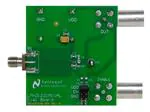
Figure 1 shows the LMH2120 Evaluation Board.
Figure 1. LMH2120 Evaluation Board
All trademarks are the property of their respective owners.
SNWA012A – July 2010 – Revised April 2013
Submit Documentation Feedback
AN-2064 LMH2120 Evaluation Board
Copyright © 2010–2013, Texas Instruments Incorporated
1
�Basic Operation
2
www.ti.com
Basic Operation
The circuit operates with a single supply form 2.7V to 5V and has an RF power detection range from −35
dBm to 5dBm. The board consist of a single LMH2120 along with external components soldered on a
printed circuit board. External supply voltages and input signals can be applied to the on-board
connectors. The supply voltage is applied with connectors P21 (VDD) and P22 (GND). The RF input
signal is applied by SMA connector P1. This RF signal is applied through an RF generator and is
connected with a 50Ω SMA cable. The detector output can be measured via BNC connector P3.
3
Configuration
The LMH2120 evaluation board can be configured via jumper settings. The device is active when EN =
High. This can be accomplished by setting the jumper J4 to VDD or by using external control on P4 by
setting the jumper J4 to EN. Since the device has an internal operating voltage of 2.5V, the voltage level
on the enable should not be higher than 3V to prevent damage to the device. Also enable voltage levels
lower than 400 mV below GND should be prevented. In both cases the ESD devices start to conduct
when the enable voltage range is exceeded and excessive current will be drawn. To guarantee a correct
operation, a voltage divider formed by R2 and R3 is present on the evaluation board. The absolute
maximum ratings are also exceeded when the enable (EN) is switched to HIGH (from shutdown to active
mode) while the supply voltage is switched off. This situation should be prevented at all times. A solution
to protect the device is the resistor R1 of 1kΩ in series with the enable input to limit the current.
An overview of the various jumper positions on the board is given in Figure 2. The settings of these
jumpers and their functions are listed in Table 1.
2
AN-2064 LMH2120 Evaluation Board
SNWA012A – July 2010 – Revised April 2013
Submit Documentation Feedback
Copyright © 2010–2013, Texas Instruments Incorporated
�Configuration
www.ti.com
Figure 2. Jumper Positions
Table 1. Jumper and Header Overview
Jumper
J4
Function
Enable
Jumper
Position
Description
1–2
Active, Connects Enable Pin to VDD (factory default configuration)
3–4
External Control, Connects Enable Pin to Enable P4
5-6
Shutdown, Connects Enable Pin to GND
SNWA012A – July 2010 – Revised April 2013
Submit Documentation Feedback
AN-2064 LMH2120 Evaluation Board
Copyright © 2010–2013, Texas Instruments Incorporated
3
�Schematic
4
www.ti.com
Schematic
The schematic of the evaluation board is shown in Figure 3.
Figure 3. Evaluation Board Schematic
5
Bill of Materials
The Bill of Material (BOM) of the evaluation board is listed in Table 2.
Table 2. Bill of Materials of the Evaluation Board
Designator
Description
Comment
C1, C2
0603 Capacitor
10 nF
C3, C4, C5
0603 Capacitor
10 pF
C6
0603 Capacitor
10 µF
J4
Header
2×3
P1
Connector
SMA
P21, P22
Connector
Banana
P3, P4
Connector
BNC
R1
0603 Resistor
1 kΩ
R2, R3
0603 Resistor
100 kΩ
R4
0603 Resistor
0Ω
TP1
Test Point
GND
U1
DSBGA
LMH2120
4
AN-2064 LMH2120 Evaluation Board
SNWA012A – July 2010 – Revised April 2013
Submit Documentation Feedback
Copyright © 2010–2013, Texas Instruments Incorporated
�Board Layout
www.ti.com
6
Board Layout
As with any other RF device, careful attention must be paid to the board layout. If the board layout isn’t
properly designed, performance might be less than can be expected for the application. The LMH2120 is
designed to be used in RF applications, having a characteristic impedance of 50Ω. To achieve this
impedance, the input of the LMH2120 needs to be connected via a 50Ω transmission line. Transmission
lines can be created on PCBs using microstrip or (grounded) coplanar waveguide (GCPW) configurations.
In order to minimize injection of RF interference into the LMH2120 through the supply lines, the PCB
traces for VDD and GND should be minimized for RF signals. This can be done by placing a small
decoupling capacitor between the VDD and GND. It should be placed as close as possible to the VDD
and GND pins of the LMH2120.
Figure 4 shows the component locations of the LMH2120 evaluation board, and Figure 5 shows the board
layout of the LMH2120 evaluation board.
Figure 4. Component Locations of Evaluation Board
SNWA012A – July 2010 – Revised April 2013
Submit Documentation Feedback
AN-2064 LMH2120 Evaluation Board
Copyright © 2010–2013, Texas Instruments Incorporated
5
�Board Layout
www.ti.com
Figure 5. Board Layout of Evaluation Board
6
AN-2064 LMH2120 Evaluation Board
SNWA012A – July 2010 – Revised April 2013
Submit Documentation Feedback
Copyright © 2010–2013, Texas Instruments Incorporated
�Measurement Setup
www.ti.com
7
Measurement Setup
The performance of the LMH2120 can be measured with the setup shown in Figure 6.
An external power supply provides a voltage of 2.7V to 5V to the evaluation board. An accurate and stable
RF Signal Generator is used to produce the test signal. Use of low loss cables is recommended to ensure
reliable measurement data. The detected output voltage can be measured with a Digital Voltage Meter
(DVM).
VDD
Power
Supply
GND
VDD
OUT
RFIN
RF Signal
Generator
LMH2120
Eval
Board
Digital
Volt
Meter
GND
Figure 6. Measurement Setup
8
Measurement Results
Figure 7 shows the output voltage versus frequency for various power levels on RFIN. The frequency
range is from 10 MHz to 10 GHz. Figure 8 shows the output voltage versus RF input power for various
frequencies.
10
10
3.5 GHz
RFIN = 0 dBm
RFIN = -5 dBm
RFIN = -15 dBm
RFIN = -20 dBm
0.1
2.6 GHz
1
RFIN = -10 dBm
VOUT (V)
VOUT (V)
1
RFIN = -25 dBm
1.9 GHz
900 MHz
0.1
50 MHz
RFIN = -30 dBm
RFIN = -35 dBm
0.01
10M
5.8 GHz
0.01
RFIN = -40 dBm
100M
1G
10G
-50
-30
-20
-10
0
10
RF INPUT POWER (dBm)
FREQUENCY (Hz)
Figure 7. Output Voltage vs. Freqency
-40
Figure 8. Output Voltage vs. RF Input Power
SNWA012A – July 2010 – Revised April 2013
Submit Documentation Feedback
AN-2064 LMH2120 Evaluation Board
Copyright © 2010–2013, Texas Instruments Incorporated
7
�IMPORTANT NOTICE
Texas Instruments Incorporated and its subsidiaries (TI) reserve the right to make corrections, enhancements, improvements and other
changes to its semiconductor products and services per JESD46, latest issue, and to discontinue any product or service per JESD48, latest
issue. Buyers should obtain the latest relevant information before placing orders and should verify that such information is current and
complete. All semiconductor products (also referred to herein as “components”) are sold subject to TI’s terms and conditions of sale
supplied at the time of order acknowledgment.
TI warrants performance of its components to the specifications applicable at the time of sale, in accordance with the warranty in TI’s terms
and conditions of sale of semiconductor products. Testing and other quality control techniques are used to the extent TI deems necessary
to support this warranty. Except where mandated by applicable law, testing of all parameters of each component is not necessarily
performed.
TI assumes no liability for applications assistance or the design of Buyers’ products. Buyers are responsible for their products and
applications using TI components. To minimize the risks associated with Buyers’ products and applications, Buyers should provide
adequate design and operating safeguards.
TI does not warrant or represent that any license, either express or implied, is granted under any patent right, copyright, mask work right, or
other intellectual property right relating to any combination, machine, or process in which TI components or services are used. Information
published by TI regarding third-party products or services does not constitute a license to use such products or services or a warranty or
endorsement thereof. Use of such information may require a license from a third party under the patents or other intellectual property of the
third party, or a license from TI under the patents or other intellectual property of TI.
Reproduction of significant portions of TI information in TI data books or data sheets is permissible only if reproduction is without alteration
and is accompanied by all associated warranties, conditions, limitations, and notices. TI is not responsible or liable for such altered
documentation. Information of third parties may be subject to additional restrictions.
Resale of TI components or services with statements different from or beyond the parameters stated by TI for that component or service
voids all express and any implied warranties for the associated TI component or service and is an unfair and deceptive business practice.
TI is not responsible or liable for any such statements.
Buyer acknowledges and agrees that it is solely responsible for compliance with all legal, regulatory and safety-related requirements
concerning its products, and any use of TI components in its applications, notwithstanding any applications-related information or support
that may be provided by TI. Buyer represents and agrees that it has all the necessary expertise to create and implement safeguards which
anticipate dangerous consequences of failures, monitor failures and their consequences, lessen the likelihood of failures that might cause
harm and take appropriate remedial actions. Buyer will fully indemnify TI and its representatives against any damages arising out of the use
of any TI components in safety-critical applications.
In some cases, TI components may be promoted specifically to facilitate safety-related applications. With such components, TI’s goal is to
help enable customers to design and create their own end-product solutions that meet applicable functional safety standards and
requirements. Nonetheless, such components are subject to these terms.
No TI components are authorized for use in FDA Class III (or similar life-critical medical equipment) unless authorized officers of the parties
have executed a special agreement specifically governing such use.
Only those TI components which TI has specifically designated as military grade or “enhanced plastic” are designed and intended for use in
military/aerospace applications or environments. Buyer acknowledges and agrees that any military or aerospace use of TI components
which have not been so designated is solely at the Buyer's risk, and that Buyer is solely responsible for compliance with all legal and
regulatory requirements in connection with such use.
TI has specifically designated certain components as meeting ISO/TS16949 requirements, mainly for automotive use. In any case of use of
non-designated products, TI will not be responsible for any failure to meet ISO/TS16949.
Products
Applications
Audio
www.ti.com/audio
Automotive and Transportation
www.ti.com/automotive
Amplifiers
amplifier.ti.com
Communications and Telecom
www.ti.com/communications
Data Converters
dataconverter.ti.com
Computers and Peripherals
www.ti.com/computers
DLP® Products
www.dlp.com
Consumer Electronics
www.ti.com/consumer-apps
DSP
dsp.ti.com
Energy and Lighting
www.ti.com/energy
Clocks and Timers
www.ti.com/clocks
Industrial
www.ti.com/industrial
Interface
interface.ti.com
Medical
www.ti.com/medical
Logic
logic.ti.com
Security
www.ti.com/security
Power Mgmt
power.ti.com
Space, Avionics and Defense
www.ti.com/space-avionics-defense
Microcontrollers
microcontroller.ti.com
Video and Imaging
www.ti.com/video
RFID
www.ti-rfid.com
OMAP Applications Processors
www.ti.com/omap
TI E2E Community
e2e.ti.com
Wireless Connectivity
www.ti.com/wirelessconnectivity
Mailing Address: Texas Instruments, Post Office Box 655303, Dallas, Texas 75265
Copyright © 2013, Texas Instruments Incorporated
�