User's Guide
SNAA053B – January 2008 – Revised May 2013
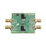
AN-1776 LMH2180 Evaluation Board in WSON
1
General Description
This evaluation board is designed to aid in the characterization of National Semiconductors' LMH2180 75
MHz dual clock buffer. This board simplifies the connection and ease of use of any oscillating input device.
Use this evaluation board as a guide for high frequency layout and as a tool to aid in device testing and
characterization.
2
Basic Operation
The LMH2180 is a device that contains two 75 MHz clock buffer amplifiers. These amplifiers are specially
designed to minimize the effects of spurious signals from the digital chip to other analog or mixed-signal
chips. The LMH2180 also minimizes the influence of varying load resistance and capacitance to the
oscillator and increases the drive capability. The buffers have a 106 V/µs internal slew rate at a supply
current of only 1.3 mA for one enabled channel and 2.3 mA for two enabled channels. Each amplifier in
the LMH2180 is capable of driving loads up to 20 pF. The input of each buffer is internally biased at 1 V.
This allows AC coupling on the input. Each buffer offers an enable pin that can be used to disable the
corresponding channel and to optimize consumption.
3
Channel Activation
Either channel can be independently enabled or shut down. The enable logic can be provided to the
evaluation board by shunting a jumper on JR1 and JR2. For the required control logic, see Table 1.
Table 1. States of LMH2180
4
Channel On
Enable1
Enable2
IN1 to OUT1
High
Don't Care
IN2 to OUT2
Don't Care
High
Layout Considerations
Careful consideration for circuitry design and PCB layout eliminates problems and optimizes the
performance of the LMH2180. It is best to have the same ground plane on the PCB for all decoupling and
other ground connections.
To ensure a clean supply voltage, it is best to place decoupling capacitors close to the LMH2180, between
VDD and VSS. On the evaluation board, capacitor C1 is placed on the bottom side.
Another important issue is the value of the components, which also determines the sensitivity to
disturbances. Resistor values have to be low enough to prevent noise coupling and large enough to avoid
a significant increase in power consumption while loading inputs or outputs to heavily.
All trademarks are the property of their respective owners.
SNAA053B – January 2008 – Revised May 2013
Submit Documentation Feedback
AN-1776 LMH2180 Evaluation Board in WSON
Copyright © 2008–2013, Texas Instruments Incorporated
1
�Layout Considerations
www.ti.com
JR1
R4 510 kÖ
JP1
GND
C5 100 nF
VDD
IN1 tp1
J1
U1A
C3
2
R3
OPT
10 nF
8
1
7
5
GND
R1
C1 10 PF
+
JP2
VDD
C2 100 nF
tp2 OUT1
J2
C4
OPT
R2
30 kÖ
VDD
IN2 tp3
J3
U1B
C6
3
R6
OPT
10 nF
4
1
6
5
GND
VDD
C8
JR2
R5
tp4 OUT2
J4
R7
30 kÖ
100 nF
C7
OPT
R8 510 kÖ
Figure 1. Schematic of the Evaluation Board
Figure 2. Layout of the Evaluation Board
The Bill of Material (BOM) of the evaluation board is given in Table 2.
2
AN-1776 LMH2180 Evaluation Board in WSON
SNAA053B – January 2008 – Revised May 2013
Submit Documentation Feedback
Copyright © 2008–2013, Texas Instruments Incorporated
�Measurement Procedure
www.ti.com
Table 2. Bill of Material
5
Designator
Description
Comment
R1, R5
0603 Resistor
0Ω
R2, R7
0603 Resistor
30 kΩ
R3, R6
0603 Resistor
Optional
R4, R8
0603 Resistor
510 kΩ
C1
Case B, Tantalum Capacitor
10 µF 16V
C2, C5, C8
0603 Capacitor
100 nF
C3, C6
0603 Capacitor
10 nF
C4, C7
0603 Capacitor
Optional
JR1, JR2
Jumper
Header 1x3
J1, J2, J3, J4
Connector
SMA
JP1
Power Connector
pin 1.5 mm, Black
JP2
Power Connector
pin 1.5 mm, Red
U1
WSON-8
LMH2180
Measurement Procedure
The performance of the LMH2180 can be measured with the setup given in Figure 3.
VDD
Power
Supply
GND
VDD
4395A
Network
Analyzer
Source
41800A
Active
Probe
JR1
J1
LMH2180
Eval
Board
4395A
Network
Analyzer
Input
tp2
GND
Figure 3. Measurement Setup
A supply voltage between 2.5 V to 5.0 V can be set by an external power supply connected to the JP2
(Red) VDD pin and JP1 (Black) GND pin. In order to test its functionality, the buffer is tested by looking at
the frequency response. Make sure to enable the buffer that has to be evaluated. The frequency response
is tested by using a network analyzer (4395A). For small signal bandwidth evaluation, the source input
should be set at −16 dBm. Be aware to measure the output of the buffer with the probe directly connected
to TP2 or TP4 to measure the highest available bandwidth.
SNAA053B – January 2008 – Revised May 2013
Submit Documentation Feedback
AN-1776 LMH2180 Evaluation Board in WSON
Copyright © 2008–2013, Texas Instruments Incorporated
3
�Measurement Results
6
www.ti.com
Measurement Results
Figure 4 shows the frequency response of the LMH2180 at 2.7 V and 5.0 V power supply and a source
input of VIN = 0.1VPP (−16 dBm @ 50 Ω).
6
2.7V
3
GAIN (dB)
0
-3
5V
-6
-9
-12
VIN = 0.1VPP
-15
100k
1M
10M
100M
FREQUENCY (Hz)
Figure 4. Frequency Response
4
AN-1776 LMH2180 Evaluation Board in WSON
SNAA053B – January 2008 – Revised May 2013
Submit Documentation Feedback
Copyright © 2008–2013, Texas Instruments Incorporated
�IMPORTANT NOTICE
Texas Instruments Incorporated and its subsidiaries (TI) reserve the right to make corrections, enhancements, improvements and other
changes to its semiconductor products and services per JESD46, latest issue, and to discontinue any product or service per JESD48, latest
issue. Buyers should obtain the latest relevant information before placing orders and should verify that such information is current and
complete. All semiconductor products (also referred to herein as “components”) are sold subject to TI’s terms and conditions of sale
supplied at the time of order acknowledgment.
TI warrants performance of its components to the specifications applicable at the time of sale, in accordance with the warranty in TI’s terms
and conditions of sale of semiconductor products. Testing and other quality control techniques are used to the extent TI deems necessary
to support this warranty. Except where mandated by applicable law, testing of all parameters of each component is not necessarily
performed.
TI assumes no liability for applications assistance or the design of Buyers’ products. Buyers are responsible for their products and
applications using TI components. To minimize the risks associated with Buyers’ products and applications, Buyers should provide
adequate design and operating safeguards.
TI does not warrant or represent that any license, either express or implied, is granted under any patent right, copyright, mask work right, or
other intellectual property right relating to any combination, machine, or process in which TI components or services are used. Information
published by TI regarding third-party products or services does not constitute a license to use such products or services or a warranty or
endorsement thereof. Use of such information may require a license from a third party under the patents or other intellectual property of the
third party, or a license from TI under the patents or other intellectual property of TI.
Reproduction of significant portions of TI information in TI data books or data sheets is permissible only if reproduction is without alteration
and is accompanied by all associated warranties, conditions, limitations, and notices. TI is not responsible or liable for such altered
documentation. Information of third parties may be subject to additional restrictions.
Resale of TI components or services with statements different from or beyond the parameters stated by TI for that component or service
voids all express and any implied warranties for the associated TI component or service and is an unfair and deceptive business practice.
TI is not responsible or liable for any such statements.
Buyer acknowledges and agrees that it is solely responsible for compliance with all legal, regulatory and safety-related requirements
concerning its products, and any use of TI components in its applications, notwithstanding any applications-related information or support
that may be provided by TI. Buyer represents and agrees that it has all the necessary expertise to create and implement safeguards which
anticipate dangerous consequences of failures, monitor failures and their consequences, lessen the likelihood of failures that might cause
harm and take appropriate remedial actions. Buyer will fully indemnify TI and its representatives against any damages arising out of the use
of any TI components in safety-critical applications.
In some cases, TI components may be promoted specifically to facilitate safety-related applications. With such components, TI’s goal is to
help enable customers to design and create their own end-product solutions that meet applicable functional safety standards and
requirements. Nonetheless, such components are subject to these terms.
No TI components are authorized for use in FDA Class III (or similar life-critical medical equipment) unless authorized officers of the parties
have executed a special agreement specifically governing such use.
Only those TI components which TI has specifically designated as military grade or “enhanced plastic” are designed and intended for use in
military/aerospace applications or environments. Buyer acknowledges and agrees that any military or aerospace use of TI components
which have not been so designated is solely at the Buyer's risk, and that Buyer is solely responsible for compliance with all legal and
regulatory requirements in connection with such use.
TI has specifically designated certain components as meeting ISO/TS16949 requirements, mainly for automotive use. In any case of use of
non-designated products, TI will not be responsible for any failure to meet ISO/TS16949.
Products
Applications
Audio
www.ti.com/audio
Automotive and Transportation
www.ti.com/automotive
Amplifiers
amplifier.ti.com
Communications and Telecom
www.ti.com/communications
Data Converters
dataconverter.ti.com
Computers and Peripherals
www.ti.com/computers
DLP® Products
www.dlp.com
Consumer Electronics
www.ti.com/consumer-apps
DSP
dsp.ti.com
Energy and Lighting
www.ti.com/energy
Clocks and Timers
www.ti.com/clocks
Industrial
www.ti.com/industrial
Interface
interface.ti.com
Medical
www.ti.com/medical
Logic
logic.ti.com
Security
www.ti.com/security
Power Mgmt
power.ti.com
Space, Avionics and Defense
www.ti.com/space-avionics-defense
Microcontrollers
microcontroller.ti.com
Video and Imaging
www.ti.com/video
RFID
www.ti-rfid.com
OMAP Applications Processors
www.ti.com/omap
TI E2E Community
e2e.ti.com
Wireless Connectivity
www.ti.com/wirelessconnectivity
Mailing Address: Texas Instruments, Post Office Box 655303, Dallas, Texas 75265
Copyright © 2013, Texas Instruments Incorporated
�