User's Guide
SNAA071A – July 2010 – Revised May 2013
AN-2028 LMH2191 Evaluation Board
1
General Description
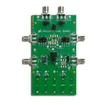
The evaluation board (Figure 1) is designed to help the evaluation of the LMH2191 Dual Channel 52 MHz
Clock Tree Driver. The LMH2191 is ideal suitable for the distribution of a system clock to peripheral
devices in mobile handsets. It provides a solution to clocking issues such as limited drive capability,
protection of the master clock from varying loads and frequency pulling effects, isolation from noisy
modules, and crosstalk isolation. It has very low phase noise which enables it to drive sensitive modules
such as Wireless LAN and Bluetooth.
The setup of the evaluation board consist of three segments:
• The TCXO oscillator that generates the clock signal that is fed to the clock buffer.
• The circuit around the LMH2191 itself. The DUT needs a stable supply to be able to operate
adequately. Furthermore there is the possibility to switch each CLK output ON and OFF separately
using a CLK request jumper setting or an external connector. Each clock output has several different
capacitive load settings which are selectable by using jumper shorts. Each clock output is also fed to
an SMA connector.
• The output buffer, that makes it possible to monitor both clock outputs or the TCXO voltage one by one
by jumper selection. The output buffer is capable to drive a 50 ohm cable in order to connect the test
board to measuring equipment.
2
Detailed Operating Description
The LMH2191 evaluation board is designed to have maximum flexibility in evaluating the LMH2191 in
various configurations. The schematic, Bill of material and board layout can be found at the end of this
application report. In the following sections, a description is given on how the circuit works and how to
setup the measurement bench. For the factory default jumper setting, refer to Section 3.
2.1
Power Supply
The board is powered by the use of banana connections, which is mostly a preferable connector type
rather than a multi pole connector. The DUT (LMH2191) uses a single supply called VBAT while the output
buffer, used for monitoring the CLK outputs and the TCXO voltage, is powered by a dual supply (called V+
& V-). The supply for the DUT ranges from 2.5V to 5.5V while the supply for the output buffer (LMH6559)
has a fixed voltage of +5V and –5V. The output voltage of the LDO is 1.8V and can be monitored on an
extra banana connector called VOUT.
2.1.1
TCXO Supply
The supply for this on-board oscillator is done by the LMH2191 via the VOUT pin. The VOUT voltage is
decoupled by C13 and C14 and is connected to jumper J8 pin 2. For normal operation, pin 1 and pin 2 are
shorten and the LDO voltage is connected to the supply pin of the TCXO. If, for any reason, an external
supply is needed, this supply voltage can be connected to J8 at the pins 3 and 4. Pin 3 is the supply of the
TCXO and pin 4 is the ground connection. (NOTE: The jumper short for the pins 1 and 2 must be
removed then).
All trademarks are the property of their respective owners.
SNAA071A – July 2010 – Revised May 2013
Submit Documentation Feedback
AN-2028 LMH2191 Evaluation Board
Copyright © 2010–2013, Texas Instruments Incorporated
1
�Detailed Operating Description
www.ti.com
Figure 1. LMH2191 Evaluation Board
2
AN-2028 LMH2191 Evaluation Board
SNAA071A – July 2010 – Revised May 2013
Submit Documentation Feedback
Copyright © 2010–2013, Texas Instruments Incorporated
�Configuration
www.ti.com
2.2
Clock Buffer LMH2191
The oscillator frequency of the TCXO or any external input frequency is fed to the SCLK_IN pin of the
LMH2191 (DUT). The input of the DUT is AC coupled because of an internal coupling capacitor of around
30 pF. This means that any DC voltage added to the input frequency doesn't disturb the DUT from
functioning.
The DUT has two clock outputs which can be switched ON or OFF independently. When both outputs are
switched OFF the part is in shutdown mode and that means that the LDO is switched OFF too. In case the
TCXO is powered by the on board LDO of the DUT, the input frequency is switched OFF too. The current
consumption drops down to zero. ON and OFF switching of the outputs is performed by both CLK_REQ
inputs. Any of the clock outputs is OFF when the matching request input is low, thus connected to ground
or a voltage below 400 mV.
The testboard provides two jumpers J5 and J6 and the SMA edge launch connectors CON9 and CON10
connected to the CLK_REQ inputs, to switch the clock outputs ON or OFF. Each clock request input has
an internal pull down resistor of 200kΩ which means that when no jumper is placed the clock output is
OFF. To force a clock output to ON the voltage on the request pin must raise above 1.4V. The voltage
used to toggle the outputs ON or OFF is VBAT or an external voltage applied to the connectors CON9 and
CON10. If an external voltage is used, the jumpers for J5 and J6 must be removed. In default
configuration VBAT is used via the short on J5 and J6 to create a HIGH or LOW level for the CLK_REQ
inputs. In case there is a need to use an external voltage to create the HIGH or LOW level on the
CLK_REQ inputs this external voltage can be applied to J4 at the pins 3 and 4. Pin 3 is the ground
connection and pin 4 is the alternate voltage for VBAT.(NOTE: The jumper short for the pins 1 and 2 must
be removed then).
Both outputs are connected to an SMA edge launch connector (CON6 and CON7) and to the header
blocks J1 and J3. These headers are used to load the output with a specific capacitive load. There are
four capacitors that can be chosen to load the output. The lowest capacitor value is 10 pF and the highest
value is 47 pF. Using these capacitors each of the outputs can have a capacitive load varying from 10 pF
to 112 pF. When no jumper is placed on J1 or J3 the capacitive load is reduced to the capacity that arises
through the connected pcb tracks. When a cable connection is made at CON6 and CON7 be aware that
the capacitive load increases, and that due to insufficient termination and 50 ohm drive capability the
output signals can deteriorate.
2.2.1
Buffering the Clock Signals
To be able to connect the output signals and the TCXO signal to measuring equipment a high bandwidth
buffer (LMH6559) is included on the pcb. The output of this buffer is connected to an SMA edge launch
connector (CON8). This buffer is capable to drive a 50 ohm cable and load with a high magnitude. The
input of the buffer consists of a 6pin header block (J2) and has a pull down resistor of 100 kΩ to assure
the output is zero in case no jumper is placed on J2. Both CLK1 and CLK2 and the TCXO output signal
are connected to J2. By placing a jumper between pin 1 and 2 the CLK1 output signal is buffered and fed
to CON8. Placing the jumper between pin 3 and 4 connects the TCXO signal to CON8 and with the
jumper placed over the pins 5 and 6 the CLK2 signal is connected to CON8. The resistor R1, placed as a
series resistor in the output line, creates the possibility to use series termination in combination with the
connected cable and load. The default value for this resistor is zero ohm.
3
Configuration
The LMH2191 evaluation board can be configured via jumper settings. An overview of the various jumper
positions on the board is given in Figure 2. The settings of these jumpers and their functions are listed in
Table 1.
SNAA071A – July 2010 – Revised May 2013
Submit Documentation Feedback
AN-2028 LMH2191 Evaluation Board
Copyright © 2010–2013, Texas Instruments Incorporated
3
�Configuration
www.ti.com
Figure 2. Jumper Positions
4
AN-2028 LMH2191 Evaluation Board
SNAA071A – July 2010 – Revised May 2013
Submit Documentation Feedback
Copyright © 2010–2013, Texas Instruments Incorporated
�Configuration
www.ti.com
Table 1. Jumper and Header Overview
Jumper
J1
J2
J3
CLK1 Capacitive Load
selection
Input signal selection for
buffer LMH6559
CLK2 Capacitive Load
selection
Description
1-2
Connects 10 pF from CLK1 to GND
3-4
Connects 22 pF from CLK1 to GND
5-6
Connects 33 pF from CLK1 to GND
7-8
Connects 47 pF from CLK1 to GND
1-2
CLK1 selected
3-4
TCXO selected
5-6
CLK2 selected
1-2
Connects 47 pF from CLK1 to GND
3-4
Connects 33 pF from CLK1 to GND
5-6
Connects 22 pF from CLK1 to GND
7-8
Connects 10 pF from CLK1 to GND
J4
CLK Request Supply
Voltage
1-2
VBAT
3-4
External Supply. 3=ground; 4=VEXT
J5
Manual CLK_REQ1
setting
Open
J6
J7
J8
(1)
Jumper
Position
Function
(1)
Manual CLK_REQ2
setting
CLK_REQ1 can be controlled externally via CON9
1-2
CLK_REQ1 = GND
2-3
CLK_REQ1 = High.
Open
CLK_REQ2 can be controlled externally via CON11
1-2
CLK_REQ2 = GND
2-3
CLK_REQ2 = High.
Frequency input selection
for SCLK_IN
1-2
External input frequency
2-3
On board TCXO
TCXO Supply
1-2
TCXO is supplied by VOUT
3-4
External Supply. 3=VEXT ; 4=ground
CON1
+5V
Positive Supply for the buffer LMH6559.
Banana Receptacle
CON2
–5V
Negative Supply for the buffer LMH6559.
Banana Receptacle
CON3
GND
Ground Connection.
Banana Receptacle
CON4
VOUT
LDO output voltage
Banana Receptacle
CON5
VBAT
Supply Voltage of the DUT
Banana Receptacle
CON6
CLK1
Clock 1 output voltage
SMA Edge Launch receptacle
CON7
CLK2
Clock 2 output voltage
SMA Edge Launch receptacle
CON8
VBUF
Buffered output voltage for CLK1, CLK2 and TCXO
SMA Edge Launch receptacle
CON9
CLK_REQ1
Connection for external signal for switching CLK1 ON or OFF
SMA Edge Launch receptacle
CON10
CLK_REQ2
Connection for external signal for switching CLK2 ON or OFF
SMA Edge Launch receptacle
CON11
Ext CLK
Connection for external clock signal.
SMA Edge Launch receptacle
TP1
+5V
Test Point Buffer Supply
TP2
–5V
Test Point Buffer Supply
TP3
GND
Test Point ground
Bold face jumper settings refer to the factory default configuration.
SNAA071A – July 2010 – Revised May 2013
Submit Documentation Feedback
AN-2028 LMH2191 Evaluation Board
Copyright © 2010–2013, Texas Instruments Incorporated
5
�Configuration
www.ti.com
Table 1. Jumper and Header Overview (1) (continued)
Jumper
6
Function
Jumper
Position
Description
TP4
GND
Test Point ground
TP5
GND
Test Point ground
TP6
GND
Test Point ground
TP7
GND
Test Point ground
TP8
VBAT
Measured at the connector side
TP9
VBAT
Measured at the DUT side
TP10
VOUT
Measured at the DUT side
TP11
VOUT
Measured at the connector side
TP12
CLK1
Clock 1 output Signal
TP13
CLK2
Clock 2 output Signal
TP14
TCXO Supply
Oscillator Supply
TP15
GND
Test Point ground
TP16
GND
Test Point ground
AN-2028 LMH2191 Evaluation Board
SNAA071A – July 2010 – Revised May 2013
Submit Documentation Feedback
Copyright © 2010–2013, Texas Instruments Incorporated
�Measurement Setup
www.ti.com
4
Measurement Setup
The performance of the LMH2191 can be measured with the setup shown in Figure 3.
To verify all the functions of the part on the evaluation board, it is recommended to have the following
equipment available:
• Multimeter
• Power Supply for dual supply of 5V and single supply of 3.5V
• Oscilloscope
• Signal Generator
Using the default settings, the TCXO is active and its signal is connected to the input of the LMP2191.
Both CLK_REQ inputs are HIGH, which means that both CLK outputs are toggling at the TCXO
frequency. The clock outputs are loaded with 33 pF and can be checked with a high impedance probe on
TP12 (CLK1) and TP13 (CLK2). The clock signals are also connected to SMA edge launch connectors
CON6 (CLK1) and CON7 (CLK2). All three signals (CLK1, CLK2, and TCXO) can be checked via another
edge launch connector (CON8) and this signal is buffered via the LMH6559 and is capable to drive a 50
ohm cable and load. Jumper J2 selects which of the three signals is chosen to appear on this connector.
The best way to check for pulse shape and bandwidth is to make use of the connector CON8.
Power Source
Multi Meter
Power Supply
VOUT
CLK Out
TCXO
Oscilloscope
BUFFER Out
LMH2191
External
CLK Input
CLK_REQ
Signal
Generator
Ext
CLK_REQ
signals
Signal
Source
Analyzer
Figure 3. Test Setup
SNAA071A – July 2010 – Revised May 2013
Submit Documentation Feedback
AN-2028 LMH2191 Evaluation Board
Copyright © 2010–2013, Texas Instruments Incorporated
7
�Schematic
5
www.ti.com
Schematic
Figure 4. Evaluation Schematic
8
AN-2028 LMH2191 Evaluation Board
SNAA071A – July 2010 – Revised May 2013
Submit Documentation Feedback
Copyright © 2010–2013, Texas Instruments Incorporated
�Bill of Material
www.ti.com
6
Bill of Material
The Bill of Material (BOM) of the evaluation board is in Table 2.
Table 2. Bill of Material
7
Designator
Description
Comment
C1, C3, C12
Case A Capacitor
4.7 µF
C2, C4, C5, C10, C11, C14
0603 Capacitor
0.1 µF
C6, C16
0603 Capacitor
10 pF
C7, C17
0603 Capacitor
22 pF
C8, C18
0603 Capacitor
33 pF
C9, C19
0603 Capacitor
47 pF
C13
Case A Capacitor
2.2 nF
C15
1206 Capacitor
0.1 µF
C20
0603 Capacitor
0.01 µF
C21
0603 Capacitor
470 pF
CON1, CON2, CON3, CON4, CON5
Connector
Banana
CON6, CON7, CON8, CON9, CON10
Connector
SMA
J1, J3
Header
4x2
J2
Header
3x2
J4, J4
Header
2x2
J5, J6, J7
Header
3x1
J9
Test Socket
8 pin
J10
Test Socket
6 pin
R1, R4, R5, R6, R7, R8, R10
0603 Resistor
0Ω
R2, R11
0603 Resistor
10 kΩ
R3
0603 Resistor
100 kΩ
R9
0603 Resistor
51Ω
TP1, TP2, TP3, TP4, TP5, TP6, TP7, TP8, TP9,
TP10, TP11, TP12, TP13, TP14, TP15, TP16
Test Point
NC
U1
IC
LMH6559
U2
IC
LMH2191
X1
TCXO - 26.000 MHz
Kyocera Corporation Part#:
KT2520F26000ACW18TAL
Board Layout
As with any other device, careful attention must be paid to the board layout. If the board isn't properly
designed, the performance of the device can be less than might be expected. Especially the input clock
trace (SCLK_IN) and output traces (CLK1/2) should be as short as possible to reduce the capacitive load
observed by the clock outputs. Also proper decoupling close to the device is necessary. Beside a
capacitor in the µF range, a capacitor of 100 nF on VBAT and VOUT is recommended close to the device.
The equivalent series resistance (ESR) of the capacitors should be sufficiently low. A standard capacitor is
usually adequate. The component locations of the evaluation board are shown in Figure 5 and Figure 6.
The copper layers of are shown in Figure 7 and Figure 8.
SNAA071A – July 2010 – Revised May 2013
Submit Documentation Feedback
AN-2028 LMH2191 Evaluation Board
Copyright © 2010–2013, Texas Instruments Incorporated
9
�Board Layout
www.ti.com
Figure 5. Component Locations Top Side
Figure 6. Component Locations Bottom Side (View from Bottom side)
10
AN-2028 LMH2191 Evaluation Board
SNAA071A – July 2010 – Revised May 2013
Submit Documentation Feedback
Copyright © 2010–2013, Texas Instruments Incorporated
�Board Layout
www.ti.com
Figure 7. Top Layer of Evaluation Board
Figure 8. Bottom Layer of Evaluation Board
SNAA071A – July 2010 – Revised May 2013
Submit Documentation Feedback
AN-2028 LMH2191 Evaluation Board
Copyright © 2010–2013, Texas Instruments Incorporated
11
�IMPORTANT NOTICE
Texas Instruments Incorporated and its subsidiaries (TI) reserve the right to make corrections, enhancements, improvements and other
changes to its semiconductor products and services per JESD46, latest issue, and to discontinue any product or service per JESD48, latest
issue. Buyers should obtain the latest relevant information before placing orders and should verify that such information is current and
complete. All semiconductor products (also referred to herein as “components”) are sold subject to TI’s terms and conditions of sale
supplied at the time of order acknowledgment.
TI warrants performance of its components to the specifications applicable at the time of sale, in accordance with the warranty in TI’s terms
and conditions of sale of semiconductor products. Testing and other quality control techniques are used to the extent TI deems necessary
to support this warranty. Except where mandated by applicable law, testing of all parameters of each component is not necessarily
performed.
TI assumes no liability for applications assistance or the design of Buyers’ products. Buyers are responsible for their products and
applications using TI components. To minimize the risks associated with Buyers’ products and applications, Buyers should provide
adequate design and operating safeguards.
TI does not warrant or represent that any license, either express or implied, is granted under any patent right, copyright, mask work right, or
other intellectual property right relating to any combination, machine, or process in which TI components or services are used. Information
published by TI regarding third-party products or services does not constitute a license to use such products or services or a warranty or
endorsement thereof. Use of such information may require a license from a third party under the patents or other intellectual property of the
third party, or a license from TI under the patents or other intellectual property of TI.
Reproduction of significant portions of TI information in TI data books or data sheets is permissible only if reproduction is without alteration
and is accompanied by all associated warranties, conditions, limitations, and notices. TI is not responsible or liable for such altered
documentation. Information of third parties may be subject to additional restrictions.
Resale of TI components or services with statements different from or beyond the parameters stated by TI for that component or service
voids all express and any implied warranties for the associated TI component or service and is an unfair and deceptive business practice.
TI is not responsible or liable for any such statements.
Buyer acknowledges and agrees that it is solely responsible for compliance with all legal, regulatory and safety-related requirements
concerning its products, and any use of TI components in its applications, notwithstanding any applications-related information or support
that may be provided by TI. Buyer represents and agrees that it has all the necessary expertise to create and implement safeguards which
anticipate dangerous consequences of failures, monitor failures and their consequences, lessen the likelihood of failures that might cause
harm and take appropriate remedial actions. Buyer will fully indemnify TI and its representatives against any damages arising out of the use
of any TI components in safety-critical applications.
In some cases, TI components may be promoted specifically to facilitate safety-related applications. With such components, TI’s goal is to
help enable customers to design and create their own end-product solutions that meet applicable functional safety standards and
requirements. Nonetheless, such components are subject to these terms.
No TI components are authorized for use in FDA Class III (or similar life-critical medical equipment) unless authorized officers of the parties
have executed a special agreement specifically governing such use.
Only those TI components which TI has specifically designated as military grade or “enhanced plastic” are designed and intended for use in
military/aerospace applications or environments. Buyer acknowledges and agrees that any military or aerospace use of TI components
which have not been so designated is solely at the Buyer's risk, and that Buyer is solely responsible for compliance with all legal and
regulatory requirements in connection with such use.
TI has specifically designated certain components as meeting ISO/TS16949 requirements, mainly for automotive use. In any case of use of
non-designated products, TI will not be responsible for any failure to meet ISO/TS16949.
Products
Applications
Audio
www.ti.com/audio
Automotive and Transportation
www.ti.com/automotive
Amplifiers
amplifier.ti.com
Communications and Telecom
www.ti.com/communications
Data Converters
dataconverter.ti.com
Computers and Peripherals
www.ti.com/computers
DLP® Products
www.dlp.com
Consumer Electronics
www.ti.com/consumer-apps
DSP
dsp.ti.com
Energy and Lighting
www.ti.com/energy
Clocks and Timers
www.ti.com/clocks
Industrial
www.ti.com/industrial
Interface
interface.ti.com
Medical
www.ti.com/medical
Logic
logic.ti.com
Security
www.ti.com/security
Power Mgmt
power.ti.com
Space, Avionics and Defense
www.ti.com/space-avionics-defense
Microcontrollers
microcontroller.ti.com
Video and Imaging
www.ti.com/video
RFID
www.ti-rfid.com
OMAP Applications Processors
www.ti.com/omap
TI E2E Community
e2e.ti.com
Wireless Connectivity
www.ti.com/wirelessconnectivity
Mailing Address: Texas Instruments, Post Office Box 655303, Dallas, Texas 75265
Copyright © 2013, Texas Instruments Incorporated
�