LMH6321
SNOSAL8D – APRIL 2006 – REVISED SEPTEMBER 2021
LMH6321 300 mA High Speed Buffer with Adjustable Current Limit
1 Features
3 Description
•
•
•
•
•
•
•
•
•
The LMH6321 is a high speed unity gain buffer that
slews at 1800 V/µs and has a small signal bandwidth
of 110 MHz while driving a 50 Ω load. It can drive
±300 mA continuously and will not oscillate while
driving large capacitive loads.
High slew rate 1800 V/μs
Wide bandwidth 110 MHz
Continuous output current ±300 mA
Output current limit tolerance ±5 mA ±5%
Wide supply voltage range 5 V to ±15 V
Wide temperature range −40°C to +125°C
Adjustable current limit
High capacitive load drive
Thermal shutdown error flag
2 Applications
Line driver
Pin driver
Sonar driver
Motor control
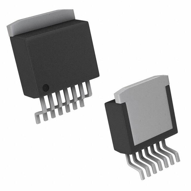
The LMH6321 is available in a space saving 8-pin SO
PowerPAD or a 7-pin DDPAK power package. The
SO PowerPAD™ package features an exposed pad
on the bottom of the package to increase its heat
sinking capability. The LMH6321 can be used within
the feedback loop of an operational amplifier to boost
the current output or as a stand alone buffer.
Table 3-1. Device Information
PACKAGE(1)
PART NUMBER
LMH6231
(1)
1
8
EF
BODY SIZE (NOM)
SO PowerPAD (8)
1.7 mm × 1.27 mm
DDPAK (7)
4.65 mm × 1.27 mm
For all available packages, see the orderable addendum at
the end of the data sheet.
NC
G=1
+
G=1
5
3
4
6 7
5
VOUT
GND
Figure 3-1. Connection Diagram: 8-Pin SO
PowerPAD
A.
V
4
2
+
6
EF
CL
-
V
1
3
VIN
VIN
-
V
V
CL
7
2
GND
VOUT
•
•
•
•
The LMH6321 features an adjustable current limit.
The current limit is continuously adjustable from 10
mA to 300 mA with a ±5 mA ±5% accuracy. The
current limit is set by adjusting an external reference
current with a resistor. The current can be easily
and instantly adjusted, as needed by connecting the
resistor to a DAC to form the reference current. The
sourcing and sinking currents share the same current
limit.
V− pin is connected to tab on back of each package.
Figure 3-2. Connection Diagram: 7-Pin DDPAK(A)
An IMPORTANT NOTICE at the end of this data sheet addresses availability, warranty, changes, use in safety-critical applications,
intellectual property matters and other important disclaimers. PRODUCTION DATA.
�LMH6321
www.ti.com
SNOSAL8D – APRIL 2006 – REVISED SEPTEMBER 2021
Table of Contents
1 Features............................................................................1
2 Applications..................................................................... 1
3 Description.......................................................................1
4 Revision History.............................................................. 2
5 Specifications.................................................................. 3
5.1 Absolute Maximum Ratings........................................ 3
5.2 Operating Ratings....................................................... 3
5.3 Thermal Information....................................................3
5.4 ±15 V Electrical Characteristics.................................. 4
5.5 ±5 V Electrical Characteristics.................................... 5
5.6 Typical Characteristics................................................ 7
6 Application Hints........................................................... 15
6.1 Buffers.......................................................................15
6.2 Supply Bypassing..................................................... 15
6.3 Load Impedence....................................................... 16
6.4 Source Inductance.................................................... 16
6.5 Overvoltage Protection............................................. 16
6.6 Bandwidth and Stability.............................................17
6.7 Output Current and Short Circuit Protection............. 17
6.8 Thermal Management...............................................18
6.9 Error Flag Operation................................................. 21
6.10 Single Supply Operation......................................... 22
6.11 Slew Rate................................................................22
7 Device and Documentation Support............................24
7.1 Receiving Notification of Documentation Updates....24
7.2 Support Resources................................................... 24
7.3 Trademarks............................................................... 24
7.4 Electrostatic Discharge Caution................................24
7.5 Glossary....................................................................24
8 Mechanical, Packaging, and Orderable Information.. 24
4 Revision History
NOTE: Page numbers for previous revisions may differ from page numbers in the current version.
Changes from Revision C (March 2013) to Revision D (September 2021)
Page
• Updated the numbering format for tables, figures, and cross-references throughout the document..................1
• Added the Device Information table....................................................................................................................1
• Removed the Thermal Resistance (θJA), (θJC), and SO PowerPAD Package details from the Operating
Ratings table.......................................................................................................................................................3
• Added the Thermal Information section..............................................................................................................3
• Added the Device and Documentation Support sections................................................................................. 24
• Added the Mechanical, Packaging, and Orderable Information section........................................................... 24
Changes from Revision B (March 2013) to Revision C (March 2013)
Page
• Changed layout of National Data Sheet to TI format........................................................................................ 22
2
Submit Document Feedback
Copyright © 2021 Texas Instruments Incorporated
Product Folder Links: LMH6321
�LMH6321
www.ti.com
SNOSAL8D – APRIL 2006 – REVISED SEPTEMBER 2021
5 Specifications
5.1 Absolute Maximum Ratings
See (1) (2)
ESD Tolerance (3)
Human Body Model
2.5 kV
Machine Model
250 V
Supply Voltage
36 V (±18 V)
Input to Output Voltage (4)
±5 V
Input Voltage
±VSUPPLY
Output Short-Circuit to GND (5)
Continuous
Storage Temperature Range
−65°C to +150°C
Junction Temperature (TJMAX)
+150°C
Lead Temperature (Soldering, 10 seconds)
260°C
(6)
Power Dissipation
CL Pin to GND Voltage
(1)
(2)
(3)
(4)
(5)
(6)
±1.2 V
Absolute Maximum Ratings indicate limits beyond which damage to the device may occur. Operating Ratings indicate conditions for
which the device is intended to be functional, but specific performance is not ensured. For specifications and the test conditions, see
the Electrical Characteristics Table.
If Military/Aerospace specified devices are required, please contact the Texas Instruments Sales Office/ Distributors for availability and
specifications.
Human Body Model is 1.5 kΩ in series with 100 pF. Machine Model is 0 Ω in series with 200 pF.
If the input-output voltage differential exceeds ±5 V, internal clamping diodes will turn on. The current through these diodes should be
limited to 5 mA max. Thus for an input voltage of ±15 V and the output shorted to ground, a minimum of 2 kΩ should be placed in
series with the input.
The maximum continuous current must be limited to 300 mA. See Section 6 for more details.
The maximum power dissipation is a function of TJ(MAX), θJA, and TA. The maximum allowable power dissipation at any ambient
temperature is PD = TJ(MAX)–TA)/θJA. See Section 6.8 of Section 6.
5.2 Operating Ratings
Operating Temperature Range
−40°C to +125°C
Operating Supply Range
5 V to ±16 V
5.3 Thermal Information
LMH6321
THERMAL
METRIC1
DDA SO Power Pad
DDAPAK
8 Pins
7 Pins
UNIT
R θJA
Junction-to-ambient thermal resistance
37.8
21.5
°C/W
R θJC(top)
Junction-to-case (top) thermal resistance
51.6
34.4
°C/W
R θJB
Junction-to-board thermal resistance
11.7
6.7
°C/W
ψ JT
Junction-to-top characterization parameter
2.5
3.2
°C/W
ψ JB
Junction-to-board characterization parameter 11.7
6.3
°C/W
R θJC(bot)
Junction-to-case (bottom) thermal resistance 3.6
1.1
°C/W
Submit Document Feedback
Copyright © 2021 Texas Instruments Incorporated
Product Folder Links: LMH6321
3
�LMH6321
www.ti.com
SNOSAL8D – APRIL 2006 – REVISED SEPTEMBER 2021
5.4 ±15 V Electrical Characteristics
The following specifications apply for Supply Voltage = ±15 V, VCM = 0, RL ≥ 100 kΩ and RS = 50 Ω, CL open, unless
otherwise noted. Italicized limits apply for TA = TJ = TMIN to TMAX; all other limits TA = TJ = 25°C.
Symbol
AV
Parameter
Voltage Gain
Min
Typ
RL = 1 kΩ, VIN = ±10 V
Conditions
0.99
0.98
0.995
RL = 50 Ω, VIN = ±10 V
0.86
0.84
0.92
Units
V/V
V/V
VOS
Input Offset Voltage
RL = 1 kΩ, RS = 0 V
±4
±35
±52
mV
IB
Input Bias Current
VIN = 0 V, RL = 1 kΩ, RS = 0 V
±2
±15
±17
μA
R.IN
Input Resistance
R.L = 50 Ω
250
kΩ
CIN
Input Capacitance
3.5
pF
RO
Output Resistance
IO = ±10 mA
5
IS
Power Supply Current
RL = ∞, VIN = 0
11
14.5
16.5
14.9
18.5
20.5
750 µA into
CL Pin
VO1
VO2
VO3
VEF
TSH
Positive Output Swing
IO = 300 mA, RS = 0 V, VIN = ±VS
Negative Output Swing
IO = 300 mA, RS = 0 V, VIN = ±VS
Positive Output Swing
RL = 1 kΩ, RS = 0 V, VIN = ±VS
Negative Output Swing
RL = 1 kΩ, RS = 0 V, VIN = ±VS
Positive Output Swing
RL = 50 Ω, RS = 0 V, VIN = ±VS
Negative Output Swing
RL = 50 Ω, RS = 0 V, VIN = ±VS
Error Flag Output Voltage
RL = ∞, VIN = 0,
EF pulled up with 5 kΩ
to +5 V
Thermal Shutdown Temperature
−11.3
13.1
12.9
−11.9
Normal
5.00
During
Thermal
Shutdown
0.25
10
3
PSSR
Power Supply Rejection Ratio
RL = 1 kΩ, VIN = 0 V,
VS = ±5 V to ±15 V
Positive
58
54
66
Negative
58
54
64
2900
VIN = ±11 V, RL = 50 Ω
1800
−3 dB Bandwidth
VIN = ±20 mVPP, RL = 50 Ω
LSBW
Large Signal Bandwidth
VIN = 2 VPP, RL = 50 Ω
HD2
2nd Harmonic Distortion
VO = 2 VPP, f = 100 kHz
VO = 2 VPP, f = 1 MHz
−12.9
−12.6
V
−10.9
−10.6
V
V
mA
dB
V/μs
110
MHz
48
MHz
RL = 50 Ω
−59
RL = 100 Ω
−70
RL = 50 Ω
−57
RL = 100 Ω
−68
Submit Document Feedback
V
°C
VIN = ±11 V, RL = 1 kΩ
BW
−10.3
−9.8
12.2
Hysteresis
EF pulled up with 5 kΩ to +5 V
mA
13.4
−13.4
11.6
11.2
Ω
11.9
168
Supply Current at Thermal
Shutdown
Slew Rate
11.2
10.8
Measure Quantity is Die (Junction)
Temperature
ISH
SR
4
Max
dBc
Copyright © 2021 Texas Instruments Incorporated
Product Folder Links: LMH6321
�LMH6321
www.ti.com
SNOSAL8D – APRIL 2006 – REVISED SEPTEMBER 2021
5.4 ±15 V Electrical Characteristics (continued)
The following specifications apply for Supply Voltage = ±15 V, VCM = 0, RL ≥ 100 kΩ and RS = 50 Ω, CL open, unless
otherwise noted. Italicized limits apply for TA = TJ = TMIN to TMAX; all other limits TA = TJ = 25°C.
Symbol
HD3
Parameter
3rd Harmonic Distortion
Conditions
VO = 2 VPP, f = 100 kHz
VO = 2 VPP, f = 1 MHz
Min
Typ
RL = 50 Ω
−59
RL = 100 Ω
−70
RL = 50 Ω
−62
RL = 100 Ω
−73
Max
Units
dBc
en
Input Voltage Noise
f ≥ 10 kHz
2.8
nV/√ Hz
in
Input Current Noise
f ≥ 10 kHz
2.4
pA/√ Hz
ISC1
Output Short Circuit Current
Source (1)
VO = 0 V,
Program Current
into CL = 25 µA
Sourcing
VIN = +3 V
4.5
4.5
10
15.5
15.5
Sinking
VIN = −3 V
4.5
4.5
10
15.5
15.5
VO = 0 V
Program Current
into CL = 750 µA
Sourcing
VIN = +3 V
280
273
295
308
325
Sinking
VIN = −3 V
280
275
295
310
325
Output Short Circuit Current
Source
RS = 0 V, VIN = +3 V(1) (2)
320
300
570
750
920
Output Short Circuit Current Sink
RS = 0 V, VIN = −3 V(1) (2)
300
305
515
750
910
CLVOS
Current Limit Input Offset Voltage
RL = 1 kΩ, GND = 0 V
±0.5
±4.0
±8.0
CLIB
Current Limit Input Bias Current
RL = 1 kΩ
CL
CMRR
Current Limit Common Mode
Rejection Ratio
RL = 1 kΩ, GND = −13 to +14 V
ISC2
mA
mA
mA
V/I Section
(1)
(2)
−0.5
−0.8
−0.2
60
56
69
mV
μA
dB
VIN = + or −4 V at TJ = −40°C.
For the condition where the CL pin is left open the output current should not be continuous, but instead, should be limited to low duty
cycle pulse mode such that the RMS output current is less than or equal to 300 mA.
5.5 ±5 V Electrical Characteristics
The following specifications apply for Supply Voltage = ±5 V, VCM = 0, RL ≥ 100 kΩ and RS = 50 Ω, CL Open, unless
otherwise noted. Italicized limits apply for TA = TJ = TMIN to TMAX; all other limits TA = TJ = 25°C.
Symbol
AV
Parameter
Voltage Gain
Min
Typ
RL = 1 kΩ, VIN = ±3 V
Conditions
0.99
0.98
0.994
RL = 50 Ω, VIN = ±3 V
0.86
0.84
0.92
Max
Units
V/V
VOS
Offset Voltage
RL = 1 kΩ, RS = 0 V
±2.5
±35
±50
mV
IB
Input Bias Current
VIN = 0 V, RL = 1 kΩ, RS = 0 V
±2
±15
±17
μA
RIN
Input Resistance
CIN
Input Capacitance
RL = 50 Ω
250
kΩ
3.5
pF
RO
Output Resistance
IOUT = ±10 mA
5
IS
Power Supply Current
RL = ∞, VIN = 0 V
10
13.5
14.7
14
17.5
19.5
750 μA into CL Pin
Ω
mA
Submit Document Feedback
Copyright © 2021 Texas Instruments Incorporated
Product Folder Links: LMH6321
5
�LMH6321
www.ti.com
SNOSAL8D – APRIL 2006 – REVISED SEPTEMBER 2021
5.5 ±5 V Electrical Characteristics (continued)
The following specifications apply for Supply Voltage = ±5 V, VCM = 0, RL ≥ 100 kΩ and RS = 50 Ω, CL Open, unless
otherwise noted. Italicized limits apply for TA = TJ = TMIN to TMAX; all other limits TA = TJ = 25°C.
Symbol
VO1
VO2
VO3
PSSR
ISC1
Parameter
IO = 300 mA, RS = 0 V, VIN = ±VS
Negative Output Swing
IO = 300 mA, RS = 0 V, VIN = ±VS
Positive Output Swing
RL = 1 kΩ, RS = 0 V, VIN = ±VS
Negative Output Swing
RL = 1 kΩ, RS = 0 V, VIN = ±VS
Positive Output Swing
RL = 50 Ω, RS = 0 V, VIN = ±VS
Negative Output Swing
RL = 50 Ω, RS = 0 V, VIN = ±VS
Power Supply Rejection Ratio
RL = 1 kΩ, VIN = 0,
VS = ±5 V to ±15 V
Output Short Circuit Current
ISC2
SR
Conditions
Positive Output Swing
Min
Typ
1.3
0.9
1.9
−1.3
3.2
2.9
−0.5
−0.1
3.5
−3.5
2.8
2.5
Max
V
V
−3.1
−2.9
3.1
−3.0
Units
V
V
−2.6
−2.4
Positive
58
54
66
Negative
58
54
64
VO = 0 V, Program Current Sourcing
into CL = 25 μA
VIN = +3 V
4.5
4.5
9
14.0
15.5
Sinking
VIN = −3 V
4.5
4.5
9
14.0
15.5
VO = 0 V, Program Current Sourcing
into CL = 750 μA
VIN = +3 V
275
270
290
305
320
Sinking
VIN = −3 V
275
270
290
310
320
V
dB
mA
Output Short Circuit Current
Source
RS = 0 V, VIN = +3 V1 2
300
470
Output Short Circuit Current Sink
RS = 0 V, VIN = −3 V1 2
300
400
Slew Rate
VIN = ±2 VPP, RL = 1 kΩ
450
VIN = ±2 VPP, RL = 50 Ω
210
90
MHz
MHz
mA
BW
−3 dB Bandwidth
VIN = ±20 mVPP, RL = 50 Ω
LSBW
Large Signal Bandwidth
VIN = 2 VPP, RL = 50 Ω
39
TSD
Thermal Shutdown
Temperature
170
Hysteresis
10
V/μs
°C
V/I Section
CLVOS
Current Limit Input Offset Voltage RL = 1 kΩ, GND = 0 V
CLIB
Current Limit Input Bias Current
RL = 1 kΩ, CL = 0 V
CL
CMRR
Current Limit Common Mode
Rejection Ratio
RL = 1 kΩ, GND = −3 V to +4 V
2.7
−0.5
−0.6
−0.2
60
56
65
+5
±5.0
mV
μA
dB
1. VIN = + or −4 V at TJ = −40°C.
2. For the condition where the CL pin is left open the output current should not be continuous, but instead,
should be limited to low duty cycle pulse mode such that the RMS output current is less than or equal to 300
mA.
6
Submit Document Feedback
Copyright © 2021 Texas Instruments Incorporated
Product Folder Links: LMH6321
�LMH6321
www.ti.com
SNOSAL8D – APRIL 2006 – REVISED SEPTEMBER 2021
5.6 Typical Characteristics
3000
60
UNDERSHOOT
2200
SLEW RATE (V/Ps)
OVERSHOOT (%)
RL = 1 k:
2600
50
40
OVERSHOOT
30
20
1800
RL = 50:
1400
1000
VIN = 100 mVPP
10
600
RL = OPEN
VS = ±15V
0
10
200
100
1k
10k
0
4
CL (pF)
RL = 1 k:
SLEW RATE (V/Ps)
2200
1800
INPUT SIGNAL
RL = 50:
1400
1000
600
200
0
4
8
12
16
20
16
20
VIN = 200 mVPP
(100 mV/DIV)
OUTPUT SIGNAL
VS = ±15V
2600
12
Figure 5-2. Slew Rate
Figure 5-1. Overshoot vs. Capacitive Load
3000
8
SUPPLY VOLTAGE (±V)
RL = 1 k:
VS = ±5V
TIME (10 ns/DIV)
24
Figure 5-4. Small Signal Step Response
INPUT AMPLITUDE (VPP)
INPUT OFFSET VOLTAGE (mV)
10
(100 mV/DIV)
INPUT SIGNAL
OUTPUT SIGNAL
Figure 5-3. Slew Rate
VIN = 200 mVPP
RL = 1 k:
VS = ±15V
25°C
85°C
9
8
125°C
-40°C
7
6
TIME (10 ns/DIV)
3
Figure 5-5. Small Signal Step Response
5
7
9
11
13
15
SUPPLY VOLTAGE (±V)
Figure 5-6. Input Offset Voltage of Amplifier vs. Supply Voltage
Submit Document Feedback
Copyright © 2021 Texas Instruments Incorporated
Product Folder Links: LMH6321
7
�LMH6321
www.ti.com
SNOSAL8D – APRIL 2006 – REVISED SEPTEMBER 2021
OUTPUT SIGNAL
RL = 50:
VS = ±5V
(100 mV/DIV)
VIN = 200 mVPP
INPUT SIGNAL
OUTPUT SIGNAL
INPUT SIGNAL
(100 mV/DIV)
5.6 Typical Characteristics (continued)
VIN = 200 mVPP
RL = 50:
VS = ±15V
TIME (10 ns/DIV)
TIME (10 ns/DIV)
OUTPUT SIGNAL
Figure 5-8. Small Signal Step Response
VS = ±15V
INPUT SIGNAL
VIN = 20 VPP
RL = 50:
VS = ±15V
(5V/DIV)
VIN = 20 VPP
RL = 1 k:
(5V/DIV)
INPUT SIGNAL
OUTPUT SIGNAL
Figure 5-7. Small Signal Step Response
TIME (5 ns/DIV)
TIME (5 ns/DIV)
VS = ±15V
INPUT SIGNAL
OUTPUT SIGNAL
RL = 1 k:
Figure 5-10. Large Signal Step Response — Leading Edge
RL = 50:
VS = ±15V
TIME (5 ns/DIV)
TIME (5 ns/DIV)
Figure 5-11. Large Signal Step Response — Trailing Edge
8
VIN = 20 VPP
(5V/DIV)
VIN = 20 VPP
(5V/DIV)
INPUT SIGNAL
OUTPUT SIGNAL
Figure 5-9. Large Signal Step Response—Leading Edge
Figure 5-12. Large Signal Step Response — Trailing Edge
Submit Document Feedback
Copyright © 2021 Texas Instruments Incorporated
Product Folder Links: LMH6321
�LMH6321
www.ti.com
SNOSAL8D – APRIL 2006 – REVISED SEPTEMBER 2021
5.6 Typical Characteristics (continued)
RL = 50:
VS = ±5V
VS = ±15V
VOUT (2V/DIV)
VOUT (0.5V/DIV)
RL = 1 k:
TIME (20 ns/DIV)
TIME (20 ns/DIV)
Figure 5-13. Large Signal Step Response
Figure 5-14. Large Signal Step Response
RL = 1 k:
VS = ±5V
VS = ±15V
VOUT (2V/DIV)
VOUT (0.5V/DIV)
RL = 50:
TIME (20 ns/DIV)
TIME (20 ns/DIV)
Figure 5-15. Large Signal Step Response
Figure 5-16. Large Signal Step Response
-20
-20
VS = ±15V
f = 1 MHz
VS = ±15V
f = 1 MHz
-30
-40
HD2 and HD3 (dBc)
HD2 and HD3 (dBc)
-30
HD2
-50
-60
HD3
-40
HD2
-50
-60
-70
-70
-80
-80
HD3
0
5
10
15
20
25
0
30
5
10
15
20
25
30
OUTPUT AMPLITUDE (VPP)
OUTPUT AMPLITUDE (VPP)
Figure 5-17. Harmonic Distortion with 50 Ω Load
Figure 5-18. Harmonic Distortion with 100 Ω Load
Submit Document Feedback
Copyright © 2021 Texas Instruments Incorporated
Product Folder Links: LMH6321
9
�LMH6321
www.ti.com
SNOSAL8D – APRIL 2006 – REVISED SEPTEMBER 2021
5.6 Typical Characteristics (continued)
-30
10000
VS = ±15V
1000
HD2
-45
NOISE
HD2 & HD3 (dBc)
-35 R = 50:
L
f = 100 kHz
-40
-50
100
10
-55
CURRENT pA/ Hz)
HD3
-60
VOLTAGE nV/ Hz)
1.0
-65
-70
0
5
10
15
20
0.1
1.0
25
10
5
5
0
0
-5
-5
-10
-15
-10
-20
VS = ±5V
-25
100k
1M
10M
100M
VS = ±15V
RL = 50:
-25
100k
1M
1G
FREQUENCY (Hz)
10M
100M
1G
FREQUENCY (Hz)
Figure 5-21. Gain vs. Frequency
Figure 5-22. Gain vs. Frequency
5
5
0
0
-5
-5
GAIN (dB)
GAIN (dB)
100k
-15
RL = 50:
-10
-15
-10
-15
VS = ±5V
VS = ±15V
RL = 1 k:
-20
100k
1M
10M
100M
1G
RL = 1 k:
-20
100k
1M
FREQUENCY (Hz)
10M
100M
1G
FREQUENCY (Hz)
Figure 5-23. Gain vs. Frequency
10
10k
Figure 5-20. Noise vs. Frequency
GAIN (dB)
GAIN (dB)
Figure 5-19. Harmonic Distortion with 50 Ω Load
-20
1k
100
FREQUENCY (Hz)
OUTPUT VOLTAGE (V)
Figure 5-24. Gain vs. Frequency
Submit Document Feedback
Copyright © 2021 Texas Instruments Incorporated
Product Folder Links: LMH6321
�LMH6321
www.ti.com
SNOSAL8D – APRIL 2006 – REVISED SEPTEMBER 2021
5.6 Typical Characteristics (continued)
14
5.2
125°C
85°C
25°C
10
5
OUTPUT IMPEDANCE (:)
SUPPLY CURRENT (mA)
VS = ±5V
-40°C
12
-40°C
8
6
4
4.8
125°C
4.6
85°C
25°C
4.4
2
0
1
3
5
7
9
11
13
15
17
4.2
19
5
7
SUPPLY VOLTAGE (±V)
9
11
13
15
17
19
SOURCING CURRENT (mA)
Figure 5-25. Supply Current vs. Supply Voltage
Figure 5-26. Output Impedance vs. Sourcing Current
5.6
5
VS = ±15V
VS = ±5V
5.4
OUTPUT IMPEDANCE (:)
OUTPUT IMPEDANCE (:)
-40°C
5.2
125°C
5
4.8
4.8
-40°C
4.6
25°C
4.4
4.2
125°C
85°C
25°C
4.6
4
5
7
9
11
13
15
17
19
5
SINKING CURRENT (mA)
7
9
11
13
15
17
19
SOURCING CURRENT (mA)
Figure 5-27. Output Impedance vs. Sinking Current
Figure 5-28. Output Impedance vs. Sourcing Current
5.2
400
VS = ±15V
5
-40°C
4.8
25°C
4.6
VS = ±15V
OUTPUT CURRENT (mA)
OUTPUT IMPEDANCE (:)
85°C
4.4
4.2
7
9
11
200
125°C
-40°C
85°C
25°C
100
85°C
125°C
5
300
13
15
17
0
25
19
125 225 325 425 525 625 725 825
PROGRAM CURRENT (PA)
SINKING CURRENT (mA)
Figure 5-29. Output Impedance vs. Sinking Current
Figure 5-30. Output Short Circuit Current — Sourcing vs.
Program Current
Submit Document Feedback
Copyright © 2021 Texas Instruments Incorporated
Product Folder Links: LMH6321
11
�LMH6321
www.ti.com
SNOSAL8D – APRIL 2006 – REVISED SEPTEMBER 2021
5.6 Typical Characteristics (continued)
400
400
VS = ±5V
300
OUTPUT CURRENT (mA)
OUTPUT CURRENT (mA)
VS = ±15V
125°C
-40°C
85°C
200
25°C
100
0
25
300
125°C
-40°C
85°C
200
25°C
100
0
25
125 225 325 425 525 625 725 825
125 225 325 425 525 625 725 825
PROGRAM CURRENT (PA)
PROGRAM CURRENT (PA)
Figure 5-31. Output Short Circuit Current — Sinking vs.
Program Current
Figure 5-32. Output Short Circuit Current — Sourcing vs.
Program Current
4
400
VS = ±5V
125°C
3.5
OUTPUT SWING (V)
OUTPUT CURRENT (mA)
85°C
300
125°C
-40°C
85°C
200
25°C
100
3
2.5
25°C
2
-40°C
1.5
1
VS = ±5V
+
VIN = V
0.5
0
25
CL = OPEN
0
125 225 325 425 525 625 725 825
0
100
PROGRAM CURRENT (PA)
200
300
Figure 5-33. Output Short Circuit Current — Sinking vs.
Program Current
14
125°C
-0.5
VS = ±15V
+
85°C
VIN = V
-1
OUTPUT SWING (V)
OUTPUT SWING (V)
13
-40°C
-2
25°C
-2.5
-3
-3.5
-4
85°C
VS = ±5V
-400
-40°C
11
9
-300
-200
-100
0
0
100
200
300
400
500
SOURCING CURRENT (mA)
SINKING CURRENT (mA)
Figure 5-35. Negative Output Swing vs. Sinking Current
12
25°C
12
125°C
CL = OPEN
-500
CL = OPEN
10
-
VIN = V
500
Figure 5-34. Positive Output Swing vs. Sourcing Current
0
-1.5
400
SOURCING CURRENT (mA)
Figure 5-36. Positive Output Swing vs. Sourcing Current
Submit Document Feedback
Copyright © 2021 Texas Instruments Incorporated
Product Folder Links: LMH6321
�LMH6321
www.ti.com
SNOSAL8D – APRIL 2006 – REVISED SEPTEMBER 2021
5.6 Typical Characteristics (continued)
-9
1000
VS = ±15V
OUTPUT SWING (V)
-10
-
CL = OPEN
-11
25°C
-40°C
-12
-13
-40°C
25°C
800
OUTPUT CURRENT (mA)
VIN = V
600
85°C
400
125°C
200
125°C
VIN = +3
85°C
-14
-500
-400
-300
-200
CL = OPEN
-100
0
0
2
4
6
SINKING CURRENT (mA)
12
14
16
18
Figure 5-38. Output Short Circuit Current — Sourcing vs.
Supply Voltage
15
-40°C
RL = 50:
25°C
13
600
85°C
125°C
400
-40°C
200
OUTPUT SWING (V)
OUTPUT CURRENT (mA)
10
SUPPLY VOLTAGE (±V)
Figure 5-37. Negative Output Swing vs. Sinking Current
800
8
11
125°C
9
85°C
7
-40°C
25°C
5
VIN = -3V
CL = OPEN
0
2
4
6
8
10
12
14
16
3
18
5
7
SUPPLY VOLTAGE (±V)
9
11
13
15
SUPPLY VOLTAGE (±V)
Figure 5-39. Output Short Circuit Current — Sinking vs. Supply
Voltage
Figure 5-40. Positive Output Swing vs. Supply Voltage
15
-3
RL = 50:
RL = 1 k:
13
-5
OUTPUT SWING (V)
OUTPUT SWING (V)
-40°C
11
125°C
9
85°C
-40°C
7
25°C
5
-7
25°C
85°C
-9
125°C
-11
-13
3
-15
5
7
9
11
13
15
5
SUPPLY VOLTAGE (±V)
7
9
11
13
15
SUPPLY VOLTAGE (±V)
Figure 5-41. Positive Output Swing vs. Supply Voltage
Figure 5-42. Negative Output Swing vs. Supply Voltage
Submit Document Feedback
Copyright © 2021 Texas Instruments Incorporated
Product Folder Links: LMH6321
13
�LMH6321
www.ti.com
SNOSAL8D – APRIL 2006 – REVISED SEPTEMBER 2021
5.6 Typical Characteristics (continued)
-3
15
VS = ±5V
INPUT OFFSET VOLTAGE (mV)
RL = 1 k:
OUTPUT SWING (V)
-5
-40°C
-7
25°C
85°C
-9
125°C
-11
-13
10
-40°C
5
25°C
0
125°C
85°C
-5
-15
5
7
9
11
13
15
-2
-3
SUPPLY VOLTAGE (±V)
Figure 5-43. Negative Output Swing vs. Supply Voltage
3
125°C
INPUT BIAS CURRENT (PA)
INPUT OFFSET VOLTGE (mV)
2
0
VS = ±15V
15
-40°C
5
25°C
-40°C
-5
85°C
-15
125°C
-2
85°C
-4
25°C
-40°C
-6
-8
125°C
-10
-25
-12
-8
-4
0
4
8
12
5
3
7
Figure 5-45. Input Offset Voltage of Amplifier vs. Common Mode
Voltage
13
15
4
VS = ±5V
VS = ±15V
25°C
-40°C
2
-40°C
1
85°C
0
-1
-2
-1
0
1
2
INPUT OFFSET VOLTAGE (mV)
4
-2
-3
11
Figure 5-46. Input Bias Current of Amplifier vs. Supply Voltage
5
3
9
SUPPLY VOLTAGE (±V)
COMMON MODE VOLTAGE (V)
INPUT OFFSET VOLTAGE (mV)
1
Figure 5-44. Input Offset Voltage of Amplifier vs. Common Mode
Voltage
25
2
3
0
25°C
-40°C
-2
125°C
-4
85°C
-6
-8
-10
-12
-8
-4
0
4
8
12
COMMON MODE VOLTAGE (V)
COMMON MODE VOLTAGE (V)
Figure 5-47. Input Offset Voltage of V/I Section vs. Common
Mode Voltage
14
0
-1
COMMON MODE VOLTAGE (V)
Figure 5-48. Input Offset Voltage of V/I Section vs. Common
Mode Voltage
Submit Document Feedback
Copyright © 2021 Texas Instruments Incorporated
Product Folder Links: LMH6321
�LMH6321
www.ti.com
SNOSAL8D – APRIL 2006 – REVISED SEPTEMBER 2021
6 Application Hints
6.1 Buffers
Buffers are often called voltage followers because they have largely unity voltage gain, thus the name has
generally come to mean a device that supplies current gain but no voltage gain. Buffers serve in applications
requiring isolation of source and load, for example, high input impedance and low output impedance (high output
current drive). In addition, they offer gain flatness and wide bandwidth.
Most operational amplifiers that meet the other given requirements in a particular application can be configured
as buffers, though they are generally more complex and are, for the most part, not optimized for unity gain
operation. The commercial buffer is a cost effective substitute for an op amp. Buffers serve several useful
functions, either in tandem with op amps or in standalone applications. As mentioned, their primary function is to
isolate a high impedance source from a low impedance load, since a high Z source cannott supply the needed
current to the load. For example, in the case where the signal source to an analog to digital converter is a
sensor, it is recommended that the sensor be isolated from the A/D converter. The use of a buffer ensures a low
output impedance and delivery of a stable output to the converter. In A/D converter applications buffers need to
drive varying and complex reactive loads.
Buffers come in two flavors: Open Loop and Closed Loop. While sacrificing the precision of some DC
characteristics, and generally displaying poorer gain linearity, open loop buffers offer lower cost and increased
bandwidth, along with less phase shift and propagation delay than do closed loop buffers. The LMH6321 is of
the open loop variety.
Figure 6-1 shows a simplified diagram of the LMH6321 topology, revealing the open loop complementary
follower design approach. Figure 6-2 shows the LMH6321 in a typical application, in this case, a 50 Ω coaxial
cable driver.
+
V
Q5
Q7
Q3
R1
D1 D3 D5 D7 D9 D11
R3
2:
Q1
VIN
VOUT
D2 D4 D6 D8D10 D12
R4
2:
Q2
R2
Q8
Q4
Q6
-
V
Figure 6-1. Simplified Schematic
6.2 Supply Bypassing
The method of supply bypassing is not critical for frequency stability of the buffer, and, for light loads, capacitor
values in the neighborhood of 1 nF to 10 nF are adequate. However, under fast slewing and large loads,
large transient currents are demanded of the power supplies, and when combined with any significant wiring
inductance, these currents can produce voltage transients. For example, the LMH6321 can slew typically at
1000 V/μs. Therefore, under a 50 Ω load condition the load can demand current at a rate, di/dt, of 20 A/μs. This
current flowing in an inductance of 50 nH (approximately 1.5” of 22 gauge wire) will produce a 1 V transient.
Thus, it is recommended that solid tantalum capacitors of 5 μF to 10 μF, in parallel with a ceramic 0.1 μF
capacitor be added as close as possible to the device supply pins.
Submit Document Feedback
Copyright © 2021 Texas Instruments Incorporated
Product Folder Links: LMH6321
15
�LMH6321
www.ti.com
SNOSAL8D – APRIL 2006 – REVISED SEPTEMBER 2021
V
R1
10 k:
TP1
EF
+
V
C2
0.1 PF
R3
R2
10 k: 1%
10 k: 1%
+
EF
VIN
CL
VOUT
LMH6321
GND
CIN
-
V
C1
1 nF
50: COAXIAL
CABLE
|
INPUT
VCL
R4
50:
OUTPUT
R6
50:
C3
0.1 PF
V
-
Figure 6-2. 50 Ω Coaxial Cable Driver with Dual Supplies
For values of capacitors in the 10 μF to 100 μF range, ceramics are usually larger and more costly than
tantalums but give superior AC performance for bypassing high frequency noise because of their very low ESR
(typically less than 10 MΩ) and low ESL.
6.3 Load Impedence
The LMH6321 is stable under any capacitive load when driven by a 50 Ω source. As shown by Figure 5-1 in
Section 5.6, worst case overshoot is for a purely capacitive load of about 1 nF. Shunting the load capacitance
with a resistor will reduce the overshoot.
6.4 Source Inductance
Like any high frequency buffer, the LMH6321 can oscillate with high values of source inductance. The worst
case condition occurs with no input resistor, and a purely capacitive load of 50 pF, where up to 100 nH of source
inductance can be tolerated. With a 50 Ω load, this goes up to 200 nH. However, a 100 Ω resistor placed in
series with the buffer input will ensure stability with a source inductances up to 400 nH with any load.
6.5 Overvoltage Protection
(Refer to the simplified schematic in Figure 6-1).
If the input-to-output differential voltage were allowed to exceed the Absolute Maximum Rating of 5 V, an internal
diode clamp would turn on and divert the current around the compound emitter followers of Q1/Q3 (D1 – D11 for
positive input), or around Q2/Q4 (D2 – D12 for negative inputs). Without this clamp, the input transistors Q1 –
Q4 would zener, thereby damaging the buffer.
To limit the current through this clamp, a series resistor should be added to the buffer input (see R1 in Figure
6-2). Although the allowed current in the clamp can be as high as 5 mA, which would suggest a 2 kΩ resistor
from a 15 V source, it is recommended that the current be limited to about 1 mA, hence the 10 kΩ shown.
The reason for this larger resistor is explained in the following: One way that the input or output voltage
differential can exceed the Absolute Maximum value is under a short circuit condition to ground while driving
the input with up to ±15 V. However, in the LMH6321 the maximum output current is set by the programmable
Current Limit pin (CL). The value set by this pin is specified to be accurate to 5 mA ±5%. If the input/output
differential exceeds 5 V while the output is trying to supply the maximum set current to a shorted condition or to
a very low resistance load, a portion of that current will flow through the clamp diodes, thus creating an error in
the total load current. If the input resistor is too low, the error current can exceed the 5 mA ±5% budget.
16
Submit Document Feedback
Copyright © 2021 Texas Instruments Incorporated
Product Folder Links: LMH6321
�LMH6321
www.ti.com
SNOSAL8D – APRIL 2006 – REVISED SEPTEMBER 2021
6.6 Bandwidth and Stability
As can be seen in the schematic of Figure 6-2, a small capacitor is inserted in parallel with the series input
resistors. The reason for this is to compensate for the natural band-limiting effect of the 1st order filter formed by
this resistor and the input capacitance of the buffer. With a typical CIN of 3.5 pF (Figure 6-2), a pole is created at
fp2 = 1/(2πR1CIN) = 4.5 MHz
(1)
This will band-limit the buffer and produce further phase lag. If used in an op amp-loop application with an
amplifier that has the same order of magnitude of unity gain crossing as fp2, this additional phase lag will
produce oscillation.
The solution is to add a small feed-forward capacitor (phase lead) around the input resistor, as shown in Figure
6-2. The value of this capacitor is not critical but should be such that the time constant formed by it and the input
resistor that it is in parallel with (RIN) be at least five times the time constant of RINCIN. Therefore,
C1 = (5RIN/R1)(CIN)
(2)
from Section 5.4, RIN is 250 kΩ.
In the case of the example in Figure 6-2, RINCIN produces a time-constant of 870 ns, so C1 should be chosen to
be a minimum of 4.4 μs, or 438 pF. The value of C1 (1000 pF) shown in Figure 6-2 gives 10 μs.
6.7 Output Current and Short Circuit Protection
The LMH6321 is designed to deliver a maximum continuous output current of 300 mA. However, the maximum
available current, set by internal circuitry, is about 700 mA at room temperature. The output current is
programmable up to 300 mA by a single external resistor and voltage source.
The LMH6321 is not designed to safely output 700 mA continuously and should not be used this way. However,
the available maximum continuous current will likely be limited by the particular application and by the package
type chosen, which together set the thermal conditions for the buffer (see Section 6.8) and could require less
than 300 mA.
The programming of both the sourcing and sinking currents into the load is accomplished with a single resistor.
Figure 6-3 shows a simplified diagram of the V to I converter and ISC protection circuitry that, together, perform
this task.
Referring to Figure 6-3, the two simplified functional blocks, labeled V/I Converter and Short Circuit Protection,
comprise the circuitry of the Current Limit Control.
The V/I converter consists of error amplifier A1 driving two PNP transistors in a Darlington configuration. The two
input connections to this amplifier are VCL (inverting input) and GND (non-inverting input). If GND is connected to
zero volts, then the high open loop gain of A1, as well as the feedback through the Darlington, will force CL, and
thus one end REXT to be at zero volts also. Therefore, as shown in Equation 3 a voltage applied to the other end
of REXT will force a current into this pin.
IEXT = VPROG/REXT
(3)
Through the VCL pin, IOUT is programmable from 10 mA to 300 mA by setting IEXT from 25 μA to 750 µA by
means of a fixed REXT of 10 kΩ and making VPROG variable from 0.25 V to 7.5 V. Thus, an input voltage VPROG
is converted to a current IEXT. This current is the output from the V/I converter. It is gained up by a factor of two
and sent to the Short Circuit Protection block as IPROG. IPROG sets a voltage drop across RSC which is applied
to the non-inverting input of error amp A2. The other input is across RSENSE. The current through RSENSE, and
hence the voltage drop across it, is proportional to the load current, through the current sense transistor QSENSE.
The output of A2 controls the drive (IDRIVE) to the base of the NPN output transistor, Q3 which is, proportional to
the amount and polarity of the voltage differential (VDIFF) between AMP2 inputs, that is, how much the voltage
across RSENSE is greater than or less than the voltage across RSC. This loop gains IEXT up by another 200, thus
ISC = 2 x 200 (IEXT) = 400 IEXT
(4)
Submit Document Feedback
Copyright © 2021 Texas Instruments Incorporated
Product Folder Links: LMH6321
17
�LMH6321
www.ti.com
SNOSAL8D – APRIL 2006 – REVISED SEPTEMBER 2021
Therefore, combining Equation 3 and Equation 4, and solving for REXT, we get
REXT = 400 VPROG/ISC
(5)
If the VCL pin is left open, the output short circuit current will default to about 700 mA. At elevated temperatures
this current will decrease.
REXTERNAL
VCL
IEXT 25 PA to 750 PA
VPROG
V/I CONVERTER
A1
GND
+
|
+
NPN OUTPUT
XTR
+
V
IOUT SENSE
XTR
IDRIVE
AMP2
QSENSE
TO INPUT
STAGE
R3
2:
SHORT CIRCUIT
PROTECTION
±VDIFF
RSENSE
200:
ILOAD
+
V
-
CONNECT TO GROUND
(FOR DUAL SUPPLIES)
OR MID RAIL FOR
SINGLE SUPPLY
RSC
400:
ISENSE
IPROG
50 PA to 1.5 mA
OUTPUT
TO LOWER OUTPUT STAGE
Only the NPN output ISC protection is shown. Depending on the polarity of VDIFF, AMP2 will turn IDRIVE either on or off.
Figure 6-3. Simplified Diagram of Current Limit Control
6.8 Thermal Management
6.8.1 Heatsinking
For some applications, a heat sink may be required with the LMH6321. This depends on the maximum power
dissipation and maximum ambient temperature of the application. To accomplish heat sinking, the tabs on
DDPAK and SO PowerPAD package may be soldered to the copper plane of a PCB for heatsinking (note that
these tabs are electrically connected to the most negative point in the circuit, for example,V−).
Heat escapes from the device in all directions, mainly through the mechanisms of convection to the air above
it and conduction to the circuit board below it and then from the board to the air. Natural convection depends
on the amount of surface area that is in contact with the air. If a conductive plate serving as a heatsink is thick
enough to ensure perfect thermal conduction (heat spreading) into the far recesses of the plate, the temperature
rise would be simply inversely proportional to the total exposed area. PCB copper planes are, in that sense, an
aid to convection, the difference being that they are not thick enough to ensure perfect conduction. Therefore,
eventually we will reach a point of diminishing returns (as seen in Figure 6-5). Very large increases in the
copper area will produce smaller and smaller improvement in thermal resistance. This occurs, roughly, for a 1
inch square of 1 oz copper board. Some improvement continues until about 3 square inches, especially for 2
oz boards and better, but beyond that, external heatsinks are required. Ultimately, a reasonable practical value
attainable for the junction to ambient thermal resistance is about 30 °C/W under zero air flow.
18
Submit Document Feedback
Copyright © 2021 Texas Instruments Incorporated
Product Folder Links: LMH6321
�LMH6321
www.ti.com
SNOSAL8D – APRIL 2006 – REVISED SEPTEMBER 2021
A copper plane of appropriate size may be placed directly beneath the tab or on the other side of the board. If
the conductive plane is placed on the back side of the PCB, it is recommended that thermal vias be used per
JEDEC Standard JESD51-5.
6.8.2 Determining Copper Area
One can determine the required copper area by following a few basic guidelines:
1. Determine the value of the circuit’s power dissipation, PD
2. Specify a maximum operating ambient temperature, TA(MAX). Note that when specifying this parameter,
it must be kept in mind that, because of internal temperature rise due to power dissipation, the die
temperature, TJ, will be higher than TA by an amount that is dependent on the thermal resistance from
junction to ambient, θJA. Therefore, TA must be specified such that TJ does not exceed the absolute
maximum die temperature of 150°C.
3. Specify a maximum allowable junction temperature, TJ(MAX), which is the temperature of the chip at
maximum operating current. Although no strict rules exist, typically one should design for a maximum
continuous junction temperature of 100°C to 130°C, but no higher than 150°C which is the absolute
maximum rating for the part.
4. Calculate the value of junction to ambient thermal resistance, θJA
5. Choose a copper area that will ensure the specified TJ(MAX) for the calculated θJA. θJA as a function of
copper area in square inches is shown in Figure 6-4.
The maximum value of thermal resistance, junction to ambient θJA, is defined as:
θJA = (TJ(MAX) - TA(MAX) )/ PD(MAX)
(6)
where
•
•
•
TJ(MAX) = the maximum recommended junction temperature
TA(MAX) = the maximum ambient temperature in the user’s environment
PD(MAX) = the maximum recommended power dissipation
Note
The allowable thermal resistance is determined by the maximum allowable heat rise , TRISE = TJ(MAX)
- TA(MAX) = (θJA) (PD(MAX)). Thus, if ambient temperature extremes force TRISE to exceed the design
maximum, the part must be de-rated by either decreasing PD to a safe level, reducing θJA, further, or,
if available, using a larger copper area.
6.8.3 Procedure
1. First determine the maximum power dissipated by the buffer, PD(MAX). For the simple case of the buffer
driving a resistive load, and assuming equal supplies, PD(MAX) is given by:
PD(MAX) = IS (2V+) + V+2/4RL
(7)
where
• IS = quiescent supply current
2. Determine the maximum allowable die temperature rise,
TR(MAX) = TJ(MAX)-TA(MAX) = PD(MAX)θJA
(8)
3. Using the calculated value of TR(MAX) and PD(MAX) the required value for junction to ambient thermal
resistance can be found:
θJA = TR(MAX)/PD(MAX)
(9)
4. Finally, using this value for θJA choose the minimum value of copper area from Figure 6-4.
Submit Document Feedback
Copyright © 2021 Texas Instruments Incorporated
Product Folder Links: LMH6321
19
�LMH6321
www.ti.com
SNOSAL8D – APRIL 2006 – REVISED SEPTEMBER 2021
6.8.4 Example
Assume the following conditions:
V+ = V− = 15 V, RL = 50 Ω, IS = 15 mA TJ(MAX) = 125°C, TA(MAX) = 85°C.
1. From Equation 7
• PD(MAX) = IS (2 V+) + V+2/4RL = (15 mA)(30 V) + 15 V2/200 Ω = 1.58 W
2. From Equation 8
• TR(MAX) = 125°C - 85°C = 40°C
3. From Equation 9
• θJA = 40°C/1.58 W = 25.3°C/W
Examining Figure 6-4, we see that we cannot attain this low of a thermal resistance for one layer of 1 oz copper.
It will be necessary to derate the part by decreasing either the ambient temperature or the power dissipation.
Other solutions are to use two layers of 1 oz foil, or use 2 oz copper (see Table 6-1), or to provide forced air flow.
One should allow about an extra 15% heat sinking capability for safety margin.
THERMAL RESISTANCE TJA (°C/W)
80
70
60
50
40
30
20
1
0
2
3
COPPER FOIL AREA (SQ. IN.)
Figure 6-4. Thermal Resistance (Typical) for 7-L DDPAK Package Mounted on 1 oz. (0.036 mm) PC Board
Foil
5
MAX POWER DISSIPATION (W)
4
3
2
1
TO-263 PACKAGE
PCB MOUNT
1 SQ. IN. COPPER
0
-40
-25
25
75
125
AMBIENT TEMPERATURE (°C)
Figure 6-5. Derating Curve for DDPAK package. No Air Flow
20
Submit Document Feedback
Copyright © 2021 Texas Instruments Incorporated
Product Folder Links: LMH6321
�LMH6321
www.ti.com
SNOSAL8D – APRIL 2006 – REVISED SEPTEMBER 2021
Table 6-1. θJA vs. Copper Area and PD for DDPAK. 1.0 oz cu Board. No Air Flow. Ambient Temperature =
24°C
Copper Area
θJA at 1.0W
(°C/W)
θJA at 2.0W
(°C/W)
1 Layer = 1”x2” cu Bottom
62.4
54.7
2 Layer = 1”x2” cu Top and Bottom
36.4
32.1
2 Layer = 2”x2” cu Top and Bottom
23.5
22.0
2 Layer = 2”x4” cu Top and Bottom
19.8
17.2
As seen in the previous example, buffer dissipation in DC circuit applications is easily computed. However,
in AC circuits, signal wave shapes and the nature of the load (reactive, non-reactive) determine dissipation.
Peak dissipation can be several times the average with reactive loads. It is particularly important to determine
dissipation when driving large load capacitance.
A selection of thermal data for the SO PowerPAD package is shown in Table 6-2. The table summarizes θJA
for both 0.5 watts and 0.75 watts. Note that the thermal resistance, for both the DDPAK and the SO PowerPAD
package is lower for the higher power dissipation levels. This phenomenon is a result of the principle of Newtons
Law of Cooling. Restated in term of heatsink cooling, this principle says that the rate of cooling and hence
the thermal conduction, is proportional to the temperature difference between the junction and the outside
environment (ambient). This difference increases with increasing power levels, thereby producing higher die
temperatures with more rapid cooling.
Table 6-2. θJA vs. Copper Area and PD for SO PowerPAD. 1.0 oz cu Board. No Airflow. Ambient
Temperature = 22°C
Copper Area/Vias
θJA at 0.5W
(°C/W)
θJA at 0.75W
(°C/W)
1 Layer = 0.05 sq. in. (Bottom) + 3 Via Pads
141.4
138.2
1 Layer = 0.1 sq. in. (Bottom) + 3 Via Pads
134.4
131.2
1 Layer = 0.25 sq. in. (Bottom) + 3 Via Pads
115.4
113.9
1 Layer = 0.5 sq. in. (Bottom) + 3 Via Pads
105.4
104.7
1 Layer = 1.0 sq. in. (Bottom) + 3 Via Pads
100.5
100.2
2 Layer = 0.5 sq. in. (Top)/ 0.5 sq. in. (Bottom) + 33 Via
Pads
93.7
92.5
2 Layer = 1.0 sq. in. (Top)/ 1.0 sq. in. (Bottom) + 53 Via
Pads
82.7
82.2
6.9 Error Flag Operation
The LMH6321 provides an open collector output at the EF pin that produces a low voltage when the Thermal
Shutdown Protection is engaged, due to a fault condition. Under normal operation, the Error Flag pin is pulled
up to V+ by an external resistor. When a fault occurs, the EF pin drops to a low voltage and then returns to V+
when the fault disappears. This voltage change can be used as a diagnostic signal to alert a microprocessor of
a system fault condition. If the function is not used, the EF pin can be either tied to ground or left open. If this
function is used, a 10 kΩ, or larger, pull-up resistor (R2 in Figure 6-2) is recommended. The larger the resistor
the lower the voltage will be at this pin under thermal shutdown. Table 6-3 shows some typical values of VEF for
10 kΩ and 100 kΩ.
Table 6-3. VEF vs. R2
At V+ = 5 V
R2 (inFigure 6-2)
At V+ = 15 V
10 kΩ
0.24 V
0.55 V
100 KΩ
0.036 V
0.072 V
Submit Document Feedback
Copyright © 2021 Texas Instruments Incorporated
Product Folder Links: LMH6321
21
�LMH6321
www.ti.com
SNOSAL8D – APRIL 2006 – REVISED SEPTEMBER 2021
6.10 Single Supply Operation
If dual supplies are used, then the GND pin can be connected to a hard ground (0 V) (as shown in Figure 6-2).
However, if only a single supply is used, this pin must be set to a voltage of one VBE (≈0.7 V) or greater, or more
commonly, mid rail, by a stiff, low impedance source. This precludes applying a resistive voltage divider to the
GND pin for this purpose. Figure 6-6 shows one way that this can be done.
+
V
LMH6321
+
GND
V
V
-
-
R1
OP AMP
+
R2
Figure 6-6. Using an Op Amp to Bias the GND Pin to ½ V+ for Single Supply Operation
In Figure 6-6, the op amp circuit pre-biases the GND pin of the buffer for single supply operation.
The GND pin can be driven by an op amp configured as a constant voltage source, with the output voltage set
by the resistor voltage divider, R1 and R2. It is recommended that These resistors be chosen so as to set the
GND pin to V+/2, for maximum common mode range.
6.11 Slew Rate
Slew rate is the rate of change of output voltage for large-signal step input changes. For resistive load, slew rate
is limited by internal circuit capacitance and operating current (in general, the higher the operating current for a
given internal capacitance, the faster is the slew rate). Figure 6-7 shows the slew capabilities of the LMH6321
under large signal input conditions, using a resistive load.
3000
VS = ±15V
SLEW RATE (V/Ps)
2600
RL = 1 k:
2200
1800
RL = 50:
1400
1000
600
200
0
4
8
12
16
20
24
INPUT AMPLITUDE (VPP)
Figure 6-7. Slew Rate vs. Peak-to-Peak Input Voltage
22
Submit Document Feedback
Copyright © 2021 Texas Instruments Incorporated
Product Folder Links: LMH6321
�LMH6321
www.ti.com
SNOSAL8D – APRIL 2006 – REVISED SEPTEMBER 2021
However, when driving capacitive loads, the slew rate may be limited by the available peak output current
according to the following expression.
dv/dt = IPK/CL
(11)
and rapidly changing output voltages will require large output load currents. For example if the part is required
to slew at 1000 V/μs with a load capacitance of 1 nF the current demand from the LMH6321 would be 1A.
Therefore, fast slew rate is incompatible with large CL. Also, since CL is in parallel with the load, the peak current
available to the load decreases as CL increases.
Figure 6-8 illustrates the effect of the load capacitance on slew rate. Slew rate tests are specified for resistive
loads and/or very small capacitive loads, otherwise the slew rate test would be a measure of the available output
current. For the highest slew rate, it is obvious that stray load capacitance should be minimized. Peak output
current should be kept below 500 mA. This translates to a maximum stray capacitance of 500 pF for a slew rate
of 1000 V/μs.
10000
SLEW RATE (V/Ps)
1000
100
10
1
0.1
0.1
1
10
100
1000
CAPACITANCE (nF)
Figure 6-8. Slew Rate vs. Load Capacitance
Submit Document Feedback
Copyright © 2021 Texas Instruments Incorporated
Product Folder Links: LMH6321
23
�LMH6321
www.ti.com
SNOSAL8D – APRIL 2006 – REVISED SEPTEMBER 2021
7 Device and Documentation Support
TI offers an extensive line of development tools. Tools and software to evaluate the performance of the device,
generate code, and develop solutions are listed below.
7.1 Receiving Notification of Documentation Updates
To receive notification of documentation updates, navigate to the device product folder on ti.com. Click on
Subscribe to updates to register and receive a weekly digest of any product information that has changed. For
change details, review the revision history included in any revised document.
7.2 Support Resources
TI E2E™ support forums are an engineer's go-to source for fast, verified answers and design help — straight
from the experts. Search existing answers or ask your own question to get the quick design help you need.
Linked content is provided "AS IS" by the respective contributors. They do not constitute TI specifications and do
not necessarily reflect TI's views; see TI's Terms of Use.
7.3 Trademarks
PowerPAD™ is a trademark of Texas Instruments.
TI E2E™ is a trademark of Texas Instruments.
All trademarks are the property of their respective owners.
7.4 Electrostatic Discharge Caution
This integrated circuit can be damaged by ESD. Texas Instruments recommends that all integrated circuits be handled
with appropriate precautions. Failure to observe proper handling and installation procedures can cause damage.
ESD damage can range from subtle performance degradation to complete device failure. Precision integrated circuits may
be more susceptible to damage because very small parametric changes could cause the device not to meet its published
specifications.
7.5 Glossary
TI Glossary
This glossary lists and explains terms, acronyms, and definitions.
8 Mechanical, Packaging, and Orderable Information
The following pages include mechanical, packaging, and orderable information. This information is the most
current data available for the designated devices. This data is subject to change without notice and revision of
this document. For browser-based versions of this data sheet, refer to the left-hand navigation.
24
Submit Document Feedback
Copyright © 2021 Texas Instruments Incorporated
Product Folder Links: LMH6321
�PACKAGE OPTION ADDENDUM
www.ti.com
29-Jul-2021
PACKAGING INFORMATION
Orderable Device
Status
(1)
Package Type Package Pins Package
Drawing
Qty
Eco Plan
(2)
Lead finish/
Ball material
MSL Peak Temp
Op Temp (°C)
Device Marking
(3)
(4/5)
(6)
LMH6321MR/NOPB
ACTIVE SO PowerPAD
DDA
8
95
RoHS & Green
SN
Level-3-260C-168 HR
-40 to 125
LMH63
21MR
LMH6321MRX/NOPB
ACTIVE SO PowerPAD
DDA
8
2500
RoHS & Green
SN
Level-3-260C-168 HR
-40 to 125
LMH63
21MR
LMH6321TS/NOPB
ACTIVE
DDPAK/
TO-263
KTW
7
45
RoHS-Exempt
& Green
SN
Level-3-245C-168 HR
-40 to 125
LMH6321TS
LMH6321TSX/NOPB
ACTIVE
DDPAK/
TO-263
KTW
7
500
RoHS-Exempt
& Green
SN
Level-3-245C-168 HR
-40 to 125
LMH6321TS
(1)
The marketing status values are defined as follows:
ACTIVE: Product device recommended for new designs.
LIFEBUY: TI has announced that the device will be discontinued, and a lifetime-buy period is in effect.
NRND: Not recommended for new designs. Device is in production to support existing customers, but TI does not recommend using this part in a new design.
PREVIEW: Device has been announced but is not in production. Samples may or may not be available.
OBSOLETE: TI has discontinued the production of the device.
(2)
RoHS: TI defines "RoHS" to mean semiconductor products that are compliant with the current EU RoHS requirements for all 10 RoHS substances, including the requirement that RoHS substance
do not exceed 0.1% by weight in homogeneous materials. Where designed to be soldered at high temperatures, "RoHS" products are suitable for use in specified lead-free processes. TI may
reference these types of products as "Pb-Free".
RoHS Exempt: TI defines "RoHS Exempt" to mean products that contain lead but are compliant with EU RoHS pursuant to a specific EU RoHS exemption.
Green: TI defines "Green" to mean the content of Chlorine (Cl) and Bromine (Br) based flame retardants meet JS709B low halogen requirements of