User's Guide
SNOA552B – July 2011 – Revised May 2013
AN-2072 LMH6522 Evaluation Board
1
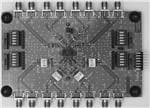
General Description
The LMH6522EVAL evaluation board, Figure 1, is designed to aid in the characterization of Texas
Instruments High Speed LMH6522 Digital Controlled Variable Gain Amplifier (DVGA).
Use the evaluation board as a guide for high frequency layout and as a tool to aid in device testing and
characterization.
2
Basic Operation
The LMH6522 DVGA has differential inputs and differential outputs. The evaluation board has been
designed to easily interface with 50Ω single ended test equipment. The LMH6522EVAL evaluation board
is shipped with input and output transformers installed to convert the DVGA differential inputs and outputs
to single ended signal paths. As built, the signal path uses the IN+ and OUT− marked connectors. The
IN− and OUT+ signal paths are grounded. The signal paths are fully symmetrical.
To preserve proper bias voltages there are DC blocking capacitors on both the input and output signal
traces. The input pins of the LMH6522 will self bias to approximately mid supply (2.5V). The output pins
need to be biased to near ground potential. Inductors are installed on the evaluation board to provide
proper output biasing. The bias current is approximately 36 mA per output pin. Capacitors between the
amplifier and the output transformer will prevent offset currents from flowing through the transformer
primary coil. Many transformers will show increased distortion products when there is a DC current flowing
through the primary coil.
Figure 1. LMH6522EVAL Evaluation Board
SPI is a trademark of Motorola, Inc..
All other trademarks are the property of their respective owners.
SNOA552B – July 2011 – Revised May 2013
Submit Documentation Feedback
AN-2072 LMH6522 Evaluation Board
Copyright © 2011–2013, Texas Instruments Incorporated
1
�Basic Operation
www.ti.com
Transformers TINA– TIND can provide both impedance matching as well as single ended to differential
conversion. The board is shipped with 2:1 impedance ratio transformers (1.4:1 Voltage ratio) that will
match 50Ω equipment with the 100Ω input impedance of the LMH6522 DVGA .
On the output side of the board are transformers TOUTA -TOUTD. The output transformers were chosen
to provide a good compromise between distortion performance and physical size. The LMH6522 is
capable of driving a wide range of load impedances. A 200 Ω load impedance was chosen for the
evaluation board to emulate performance with a 100 Ω back terminated filter. Other configurations are
possible with minor rework of the evaluation board.
Capacitors CCOA± through CCOD± are installed to isolate the DVGA outputs from the output transformer
primary windings. The output resistors are 40.2 Ω matching resistors. The output impedance of the
LMH6522 amplifier is very low (10Ω @ 50MHz), and the 40.2 Ω resistors provide termination for the 100 Ω
load presented by the transformer when the evaluation board is connected to 50 Ω test equipment. The
JTX–2–10T output transformers have a 1:2 impedance ratio.
The LMH6522 DVGA is configured to have a maximum gain of 26dB. The transformers and matching
resistors contribute a loss of approximately 7.5 dB. Gain through the board should measure approximately
18.6 dB.
Zoomed in portions of the input and output schematics are shown above in Figure 2 and Figure 3. These
schematics show that the evaluation board, as shipped, has been built with single ended inputs and
outputs. The full signal path schematic is shown in Figure 10 and the full evaluation board schematic,
including the digital control portions is available in .PDF format upon request.
LOAGND
1.0E-6 PH
OUTAROAG0CTOA+
CCOA+
OUTA1_ P
3
CCTOA
0.01 PF
CCOACTOA-
OUTA1_ N
1000 pF
TOUTA
COA+
4
2
1
0.01 PF
C0A-
6
JTX2-10
0.01 PF
0.01 PF
ROAG0+
0
GND
OUTA+
OUTA- 1
5
4
3
2
GND
OUTA+ 1
0
5
4
3
2
LOA+
1.0E-6 PH
GND
GND
OUTA+
OUTA-
44
OUTA_P
LOB+
43
OUTA_N
1.0E-6 PH
DVGA
LMH6522
Figure 2. Output Schematic
2
AN-2072 LMH6522 Evaluation Board
SNOA552B – July 2011 – Revised May 2013
Submit Documentation Feedback
Copyright © 2011–2013, Texas Instruments Incorporated
�Using with Differential Sources or Loads
www.ti.com
GND
INA+
INA+
0
RIAG0-
CIA+
2
3
4
5
1
6
INAINA-
CCTIA
3
4
0.01 PF
CTIA-
1000 pF
TC2-1T
0.01 PF
0.01 PF
RIAG0+
0
GND
2
3
4
5
1
CTIA+
1
2
0.01 PF
CIA-
GND
TINA
GND
GND
INA_P
2
INA_ N
3
INA+
INA-
DVGA
LMH6522
Figure 3. Input Schematic
3
Using with Differential Sources or Loads
The LMH6522EVAL board was designed to be easily modified by the customer for fully differential
operation. To modify the board for differential operation it is necessary to remove the transformers and the
resistors that ground the unused signal paths. Next, add coupling capacitors on the IN- and OUT+ signal
lines, and finally place shorting jumpers across the appropriate transformer pads. At this point the
LMH6522EVAL board will be configured for a 100 Ω differential signal path.
Other load conditions can also be easily matched by placing appropriate components on existing pads on
the evaluation board. When changing components remember to keep the input path AC coupled so that
the input common mode voltage is preserved.
4
Gain Control
For ease of use, banks of DIP switches are set up to control gain settings. For high speed interfacing to a
logic analyzer there are also 0.1” header strips. The pin functions for these headers are shown in Table 1.
For detailed instructions on the pin functions, see LMH6522 High Performance Quad DVGA (SNOSB53).
The dip switches settings will impact the on-board impedance for the J1 header pins. With the dip
switches should be set to the OPEN position the header pins are unterminated. When the dip switches are
closed the header pins are terminated with 49.9 Ω resistors. This would be the preferred setting for most
high speed signal interfaces. For the absolute maximum voltage and current ratings of the digital pins, see
the device-specific data sheet.
Table 1. Header Jack Pin Assignments (CONA. CONB, CONC, COND)
(Pin 1 is pin closest to input connectors)
Header Pin
Parallel Function
1
Address bit 0
2
Address bit 1
3
Address bit 2
4
Address bit 3
5
Address bit 4
6
Ground
7
Enable (Tri State Pin)
SNOA552B – July 2011 – Revised May 2013
Submit Documentation Feedback
AN-2072 LMH6522 Evaluation Board
Copyright © 2011–2013, Texas Instruments Incorporated
3
�SPI™ Compatible Gain Control Using the SPISU2 Card
5
www.ti.com
SPI™ Compatible Gain Control Using the SPISU2 Card
The LMH6522_EVAL board can easily be controlled in the serial mode using a Texas Instruments SPISU2
USB to SPI controller card. This card and the required software are available on the TI website. Directions
for installing the USB control software and evaluation board drivers are in the user's guide available in the
document, SNLU086.
To use the SPI card, the LMH6522 DVGA must be put into serial mode. This is done by placing a shorting
block on the MODE jumper pins which are located near the power connectors in the center of the board.
Once this shorting block is in place the switches on the SWA switch block all need to be put in the OFF
position. If the switches are in the ON position the digital lines will be grounded and the SPISU2 card will
not be able to communicate with the DVGA.
Once the SPUSI2 board drivers and TinyI2CSPI software are installed, connect the SPUSI2 board directly
onto the LMH6522_EVAL double-row header (J1) by aligning pin 1 as shown in Figure 4. Plug the USB
cable into the SPISU2 card and the host PC. Start the TinyI2CSPI software and load the LMH6522 profile
as shown in Figure 5. Additional commands can be generated by changing the data in the MOSI column.
For details on the data to be sent to the DVGA registers, see the LMH6522 data sheet (SNOSB53). The
example SPI commands are a good starting point for generating the desired commands.
SPISU2 Header Pins
1
Chip Select
2
Ground
3
Clock
4
N/A
5
Serial Data Out (MISO)
6
N/A
7
Serial Data IN (MOSI)
8 -14
4
Serial Function
N/A
AN-2072 LMH6522 Evaluation Board
SNOA552B – July 2011 – Revised May 2013
Submit Documentation Feedback
Copyright © 2011–2013, Texas Instruments Incorporated
�SPI™ Compatible Gain Control Using the SPISU2 Card
www.ti.com
Figure 4. SPISU2 Card Connected to LMH6522EVAL Board
SNOA552B – July 2011 – Revised May 2013
Submit Documentation Feedback
AN-2072 LMH6522 Evaluation Board
Copyright © 2011–2013, Texas Instruments Incorporated
5
�Additional Design Tools
www.ti.com
Figure 5. TinyI2CSPI Settings
6
Additional Design Tools
The RD-179: High-IF Sub-sampling Receiver Subsystem board (SP16160CH1RB) is also available. This
reference design includes the ADC16DV160 ADC, the LMH6517 DVGA, and the LMK04031B precision
clock conditioner. Power regulation, filters and controlled impedance board layout are all provided in this
reference design. Please visit the TI website for further details.
7
Board Layout
The LMH6522EVAL board has been designed to provide excellent signal integrity and has been thermally
enhanced to provide for excellent heat dissipation. The LMH6522EVAL board has balanced differential
signal traces as well as provision for using single ended test equipment.
The LMH6522 DVGA dissipates approximately 2.4W of power. To keep the amplifier cool, the
LMH6522EVAL board uses eight layers of copper, many of which are solid ground planes connected
directly to the LMH6522 exposed thermal pad. This provides excellent heat dissipation and eliminates the
need for a heat sink. The board design files (in GERBER) format are available upon request.
6
AN-2072 LMH6522 Evaluation Board
SNOA552B – July 2011 – Revised May 2013
Submit Documentation Feedback
Copyright © 2011–2013, Texas Instruments Incorporated
�Board Layout
www.ti.com
Figure 6. Evaluation Board Top Layer
Figure 7. Layout Layer 2 (Showing Metal Removed from Under Input and Output Pins)
SNOA552B – July 2011 – Revised May 2013
Submit Documentation Feedback
AN-2072 LMH6522 Evaluation Board
Copyright © 2011–2013, Texas Instruments Incorporated
7
�Board Layout
www.ti.com
Figure 8. Evaluation Board Bottom Layer
8
AN-2072 LMH6522 Evaluation Board
SNOA552B – July 2011 – Revised May 2013
Submit Documentation Feedback
Copyright © 2011–2013, Texas Instruments Incorporated
�Board Layout
www.ti.com
V+
C25
A/R
R1
301
A2/CS
A1/CLK
A4/SDO
A3/SDI
SPUS12
1
3
5
7
9
11
13
1
2
V+
2
4
6
8
10
12
14
RA0
JA0V+
49.9
1
2
3
4
5
6
7
ENBA
A0
A1/CLK
A2/CS
A3/SDI
A4/SDO
RA1
SWA
10
9
8
7
6
49.9
RA2
A0
A1/CLK
A2/CS
A3/SDI
A4/SDO
49.9
RA3
206-5
ENA
49.9
RA4
ENBA
CON A
49.9
GND
1
2
4
COM
RAE
49.9
V+
SS14MDP2
GND
Figure 9. Logic Header Schematic
SNOA552B – July 2011 – Revised May 2013
Submit Documentation Feedback
AN-2072 LMH6522 Evaluation Board
Copyright © 2011–2013, Texas Instruments Incorporated
9
�Signal Path Schematic
8
www.ti.com
Signal Path Schematic
V+
V+
RIDG00
2
3
4
5
6
INDIND-
A3/SDI
1000 pF
RIDG0+
0
GND
+5VC
GND
ENBD
GND
+5VD
IND+
OUTD+
IND-
OUTD-
GND
D4
24
25
26
27
D2
D3
C0A+
JTX-2-10T+
0.01 PF
5
4
3
2
0.01 PF
0.01 PF
ROAG0+
0
GND
OUTA+
OUTA+ 1
5
4
3
2
GND
D1
1
43
OUTA_N
CTOB+
42
41
40.2
ENBA
ENBA
0.01 PF
CCOB-
40.2
0.01 PF
38
OUTB_N
37
ENBB
36
ENBC
35
OUTC_P
34
OUTC_N
ROBG00
GND
OUTB1_ P
4
CCTOB
OUTB1_ N
1000 pF
TOUTB
5
COB3
0.01 PF
2
6
COB+
1
JTX-2-10T
0.01 PF
ROBG0+
0
GND
ENBB
GND
GND
OUTCROCG00
COC-
GND
ENBD
CTOC+
CCOC+
40.2
0.01 PF
CTOC-
CCOC-
40.2
0.01 PF
ENBD
31
30
OUTD_P
29
OUTD_N
28
GND
OUTB+
OUTB+ 1
ENBC
33
32
OUTBOUTB- 1
5
4
3
2
OUTB_P
CCOB+
CTOB-
40
39
GND
GND
1.0E-6 PH
1.0E-6 PH
5
4
3
2
OUTA_P
LOB-
4
CCTOC
OUTC1_ N
1000 pF
TOUTC
3
5
2
6
1
0.01 PF
COC+
JTX-2-10T
LOC+
LOC-
D4
OUTC1_ P
0.01 PF
ROCG0+
0
GND
1.0E-6 PH
1.0E-6 PH
OUTC- 1
5
4
3
2
OUTC-
A4
GND
OUTC+
OUTC+ 1
V+
GND
GND
CCP1
GND
OUTD-
1000 pF
RODG00
COD-
GND
0.01 PF
CTID0.01 PF
2
6
5
4
3
2
INC-
A4/SDO
A2/CS
OUTC+
GND
1000 pF
3
GND
LOB+
44
CCTID
TC2-1T
0.01 PF
ENBC
INC+
OUTA1_ N
TOUTA
5
CDP1
1000 pF
CCP0
0.01 PF
CDP0
0.01 PF
CTOD+
40.2
CTOD-
GND
LOD-
LOD+
1.0E-6 PH
1.0E-6 PH
40.2
CCOD+
OUTD1_ P
4
CCTOD
0.01 PF
CDOB- OUTD1_ N
1000 pF
TOUTD
2
6
1
0.01 PF
COD+
JTX-2-10T
0.01 PF
GND
OUTD- 1
3
5
0.01 PF
RODG0+
0
2
3
4
5
1
CTID+
ENBB
55
EP
GND
4
CCTOA
1000 pF
45
1
3
4
40.2
OUTA1_ P
OUTA- 1
GND
OUTD+
OUTD+ 1
5
4
3
2
GND
TIND
2
0.01 PF
CID-
GND
C0
IND+
CID+
1000 pF
CAP1
D4
18
A2/CS
A3
GND
A3/SDI
46
17
GND
GND
A0
47
IND_ N
GND
IND+
CTOA-
CCOA-
D3
16
OUTB-
D2
0.01 PF
RICG0+
0
GND
1
0.01 PF
CBP0
D3
0.01 PF
IND_ P
OUTB+
INB-
D0
INC-
15
2
3
4
5
1
1000 pF
TC2-1T
0.01 PF
CTIC-
INB+
23
INC-
3
4
CCTIC
+5VB
C4
GND
14
ENBA
D2
2
0.01 PF
CIC-
13
CTIC+
1
GND
C0
2
3
4
5
TINC
6
A1/CLK
A2
12
DVGA
LMH6522
MODE
D1
INC_ N
+5VA
D1
RICG00
A1/CLK
A1
11
INC+
CIC+
B4
A0
48
10
INC_ P
A0
49
8
OUTA-
D0
INB_N
A4/SDO
GND
D0
7
GND
GND
B3
B4
GND
INB_P
B4
50
0.01 PF
GND
INC+
0.01 PF
GND
OUTA+
C4
5
6
RIBG0+
0
B2
B3
51
0.01 PF
CTIB-
9
1
CCOA+
40.2
0.01 PF
GND
INA-
C4
1000 pF
OUTAROAG00
COA-
GND
CTOA+
CAP0
CBP1
INA+
22
INB-
4
TC2-1T
0.01 PF
3
CCTIB
2
3
4
5
1
3
4
INA_ N
GND
C3
INB-
CTIB+
1
2
0.01 PF
CIB-
GND
GND
TINB
6
2
21
2
3
4
5
CIB+
INA_P
C3
RIBG00
C2
GND
20
INB+
C3
1
INB+
C2
GND
B0
RMODE
200
B3
B2
GND
1
B1
B1
52
V+
B2
MODE
B0
GND
53
RIAG0+
0
B0
0.01 PF
54
0.01 PF
19
INA-
TC2-1T
GND
2
3
4
5
1
1000 pF
0.01 PF
CTIA-
C0
INA-
3
4
CCTIA
C2
2
C1
GND
CTIA+
V+
1
B1
TINA
6
C1
CIA+
0.01 PF
CIA-
LOAGND
1.0E-6 PH
1.0E-6 PH
5
4
3
2
RIAG00
C1
GND
1
2
INA+
2
3
4
5
1
LOA+
DP1
10BQ100TRPBF
+ CP1
0.78V
10 PF
GND TPG1
INA+
GND
GND
GND
GND
GND
Figure 10. Signal Path Schematic
10
AN-2072 LMH6522 Evaluation Board
SNOA552B – July 2011 – Revised May 2013
Submit Documentation Feedback
Copyright © 2011–2013, Texas Instruments Incorporated
�IMPORTANT NOTICE
Texas Instruments Incorporated and its subsidiaries (TI) reserve the right to make corrections, enhancements, improvements and other
changes to its semiconductor products and services per JESD46, latest issue, and to discontinue any product or service per JESD48, latest
issue. Buyers should obtain the latest relevant information before placing orders and should verify that such information is current and
complete. All semiconductor products (also referred to herein as “components”) are sold subject to TI’s terms and conditions of sale
supplied at the time of order acknowledgment.
TI warrants performance of its components to the specifications applicable at the time of sale, in accordance with the warranty in TI’s terms
and conditions of sale of semiconductor products. Testing and other quality control techniques are used to the extent TI deems necessary
to support this warranty. Except where mandated by applicable law, testing of all parameters of each component is not necessarily
performed.
TI assumes no liability for applications assistance or the design of Buyers’ products. Buyers are responsible for their products and
applications using TI components. To minimize the risks associated with Buyers’ products and applications, Buyers should provide
adequate design and operating safeguards.
TI does not warrant or represent that any license, either express or implied, is granted under any patent right, copyright, mask work right, or
other intellectual property right relating to any combination, machine, or process in which TI components or services are used. Information
published by TI regarding third-party products or services does not constitute a license to use such products or services or a warranty or
endorsement thereof. Use of such information may require a license from a third party under the patents or other intellectual property of the
third party, or a license from TI under the patents or other intellectual property of TI.
Reproduction of significant portions of TI information in TI data books or data sheets is permissible only if reproduction is without alteration
and is accompanied by all associated warranties, conditions, limitations, and notices. TI is not responsible or liable for such altered
documentation. Information of third parties may be subject to additional restrictions.
Resale of TI components or services with statements different from or beyond the parameters stated by TI for that component or service
voids all express and any implied warranties for the associated TI component or service and is an unfair and deceptive business practice.
TI is not responsible or liable for any such statements.
Buyer acknowledges and agrees that it is solely responsible for compliance with all legal, regulatory and safety-related requirements
concerning its products, and any use of TI components in its applications, notwithstanding any applications-related information or support
that may be provided by TI. Buyer represents and agrees that it has all the necessary expertise to create and implement safeguards which
anticipate dangerous consequences of failures, monitor failures and their consequences, lessen the likelihood of failures that might cause
harm and take appropriate remedial actions. Buyer will fully indemnify TI and its representatives against any damages arising out of the use
of any TI components in safety-critical applications.
In some cases, TI components may be promoted specifically to facilitate safety-related applications. With such components, TI’s goal is to
help enable customers to design and create their own end-product solutions that meet applicable functional safety standards and
requirements. Nonetheless, such components are subject to these terms.
No TI components are authorized for use in FDA Class III (or similar life-critical medical equipment) unless authorized officers of the parties
have executed a special agreement specifically governing such use.
Only those TI components which TI has specifically designated as military grade or “enhanced plastic” are designed and intended for use in
military/aerospace applications or environments. Buyer acknowledges and agrees that any military or aerospace use of TI components
which have not been so designated is solely at the Buyer's risk, and that Buyer is solely responsible for compliance with all legal and
regulatory requirements in connection with such use.
TI has specifically designated certain components as meeting ISO/TS16949 requirements, mainly for automotive use. In any case of use of
non-designated products, TI will not be responsible for any failure to meet ISO/TS16949.
Products
Applications
Audio
www.ti.com/audio
Automotive and Transportation
www.ti.com/automotive
Amplifiers
amplifier.ti.com
Communications and Telecom
www.ti.com/communications
Data Converters
dataconverter.ti.com
Computers and Peripherals
www.ti.com/computers
DLP® Products
www.dlp.com
Consumer Electronics
www.ti.com/consumer-apps
DSP
dsp.ti.com
Energy and Lighting
www.ti.com/energy
Clocks and Timers
www.ti.com/clocks
Industrial
www.ti.com/industrial
Interface
interface.ti.com
Medical
www.ti.com/medical
Logic
logic.ti.com
Security
www.ti.com/security
Power Mgmt
power.ti.com
Space, Avionics and Defense
www.ti.com/space-avionics-defense
Microcontrollers
microcontroller.ti.com
Video and Imaging
www.ti.com/video
RFID
www.ti-rfid.com
OMAP Applications Processors
www.ti.com/omap
TI E2E Community
e2e.ti.com
Wireless Connectivity
www.ti.com/wirelessconnectivity
Mailing Address: Texas Instruments, Post Office Box 655303, Dallas, Texas 75265
Copyright © 2013, Texas Instruments Incorporated
�