User's Guide
SNOA516B – February 2008 – Revised May 2013
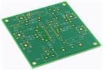
AN-1808 LMH730033 Evaluation Board
1
Complete Schematic
Figure 1 shows the complete evaluation circuit implemented on this board. The primary connections are
shown with solid lines, while several optional circuit connections are shown with dashed lines. The shaded
area is inside the device.
+
In2
V
C8
C1
R6
R6 '
+
R14
C3
C5
+VIN
R5
3
X1
BUFFER
V
-
R7
R1
14
12
+ RG
GAIN
ADJUST
4
-VIN
VOUT
-
R3
- RG
1
OUTPUT
AMPLIFIER
+
5
6
2
X1
BUFFER
9
R11
7
10
R8
8
C6
R2
R4
C4
+
R12
C2
+5V
R9
C7
R13
V
+
V
-
V
VG
R10
-
Figure 1. External Components and Amplifier Internal Block Diagram
All trademarks are the property of their respective owners.
SNOA516B – February 2008 – Revised May 2013
Submit Documentation Feedback
AN-1808 LMH730033 Evaluation Board
Copyright © 2008–2013, Texas Instruments Incorporated
1
�Basic Connection
2
www.ti.com
Basic Connection
Figure 2 represents the simplest board configuration. The specific resistor values depicted here configure
the device with a maximum gain of 9.9 V/V:
+
+
V
+VIN
1
13
14
NC
11
3
4
R1
50:
C6
0.1 PF
C2
0.1 PF
C3
6.8 PF
R7
1 k:
R8
50:
12
R3
174:
10
VOUT
9
5
6
R2
50:
2
8
VG
7
+
R4
50:
C4
6.8 PF
-
V
C1
0.1 PF
C5
0.1 PF
Figure 2. Basic Connection
The circuit of Figure 2 implements a non-inverting variable-gain amplifier with a 50 Ω input impedance
(R1), a 50 Ω output impedance (R8), and a maximum gain of 9.9 V/V (1.72*(R7/R3)). Recognizing the
combination of the 50 Ω series output resistor and the 50 Ω load results in a voltage divider, the gain to
this match load is one half of the maximum device gain setting, that is, 4.9 V/V (13.9 dB). The inverting
input (In-) is ground-referenced through 50 Ω while the output amplifier's non-inverting input is groundreferenced at pin 9 through R11 (not shown, replace R11 on board with a short).
3
Summing Signals and Offsets into the Output Stage
The output amplifier's inverting node (pin 12) is available to introduce any additional signals or offsets into
the output. Since pin 12 is a virtual ground, additional signals may be summed into the node without a
substantial impact on the signal current flowing from the adjustable-gain path. Briefly, adding an additional
impedance on the output amplifier will result in a slight bandwidth reduction of the output amplifier and an
increase in the noise gain for the output amplifier's non-inverting input noise voltage. For a more thorough
discussion of current feedback amplifiers in inverting summing applications, see OA-13 Current Feedback
Loop Gain Analysis and Performance Enhancement (SNOA366).
2
AN-1808 LMH730033 Evaluation Board
SNOA516B – February 2008 – Revised May 2013
Submit Documentation Feedback
Copyright © 2008–2013, Texas Instruments Incorporated
�Summing Signals and Offsets into the Output Stage
www.ti.com
Figure 3 shows an example of using the optional components on the board to sum in a high-speed signal
with a gain of −2 to the output pin ( or −1 to the matched 50 Ω load).
50:
INPUT
IN2
50:
SOURCE
R6
54.9:
R5
500:
R7
1 k:
12
10
R8
50:
50:
LOAD
Figure 3. Summing a High-Speed Signal Into the Output
Note that R6 can be used in either of two locations on this board. In Figure 3 R6 is positioned as part of the
output op amp's inverting input (In2) termination. Alternatively, it can be positioned to pick off the wiper
voltage of an offset-adjust pot (R14Figure 1) that is to be fed into the inverting node of the output amplifier.
Figure 4 shows this application where an output offset, independent of the gain adjustment stage, is
introduced into the inverting node of the output amplifier.
+5V
R6
2 k:
R5
2 k:
R14
10 k:
-5V
R7
1 k:
AV = ¼ AT POT EXTREMES
±1.25 OUTPUT DC VOLTAGE
ADJUSTMENT RANGE
Figure 4. Summing in an Output DC Offset
SNOA516B – February 2008 – Revised May 2013
Submit Documentation Feedback
AN-1808 LMH730033 Evaluation Board
Copyright © 2008–2013, Texas Instruments Incorporated
3
�Nulling the Output DC Offset
4
www.ti.com
Nulling the Output DC Offset
There are several factors contributing to the output offset voltage; the differential input buffer, and the
multiplier core and the output amplifier. The offsets produced by the input buffer and the output amplifier
can be nulled with appropriate external circuitry. It will not be possible to completely null the offset effects
of the multiplier core because of its non-linear nature. As a result, a small non-linear DC offset voltage
gain over the adjustment range will always be present at the output of the device. Figure 5 shows the
required external circuitry necessary to add the appropriate nulling offsets at both the input buffer and the
output amplifier.
+
V
SUPPLIES AND DE-COUPLING TO
AMPLIFIER NOT SHOWN
R6
2 k:
R5
2 k:
+VIN
R1
50:
V
3
4
R10
10 k:
C7
0.1 PF
V
R2
50:
5
6
-
V
VOUT
12
10
R3
+
R9
1 k:
R7
1 k:
R14
10 k:
2
GAIN ADJUST
-
Figure 5. Input and Output Stage DC Nulling
The output stage offset should be trimmed prior to the input stage. With the gain adjust pin set at minimum
gain (maximum attenuation), the output stage offset may be nulled independently from the input stage. R14
should be adjusted to yield the desired output error voltage (typically
很抱歉,暂时无法提供与“LMH730033/NOPB”相匹配的价格&库存,您可以联系我们找货
免费人工找货