LMH7322
www.ti.com
SNOSAU8I – MARCH 2007 – REVISED MARCH 2013
LMH7322 Dual 700 ps High Speed Comparator with RSPECL Outputs
Check for Samples: LMH7322
FEATURES
DESCRIPTION
•
•
•
•
•
•
The LMH7322 is a dual comparator with 700 ps
propagation delay, low dispersion of 75 ps and an
input voltage range that extends from VCC-1.5V to
VEE. The devices can be operated from a wide supply
voltage range of 2.7V to 12V. The adjustable
hysteresis adds flexibility and prevents oscillations.
Both the outputs and latch inputs of the LMH7322 are
RSPECL compatible. When used in combination with
a VCCO supply voltage of 2.5V the outputs have LVDS
compatible levels.
1
2
•
•
•
(VCCI = +5V, VCCO = +5V)
Propagation Delay 700 ps
Overdrive Dispersion 20 mV-1V 75 ps
Fast Rise and Fall Times 160 ps
Wide Supply Range 2.7V to 12V
Input Common Mode Range Extends 200 mV
Below Negative Rail
Adjustable Hysteresis
(RS)PECL Outputs (see Application
Information)
(RS)PECL Latch Inputs (see Application
Information)
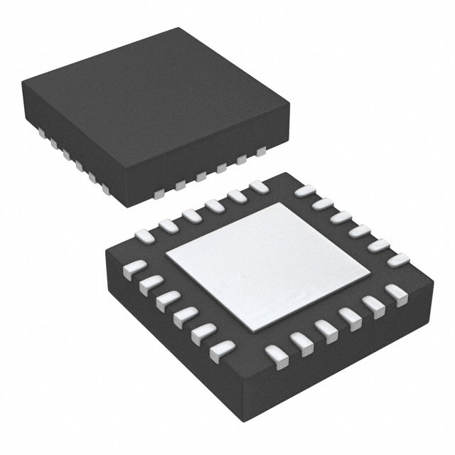
The LMH7322 is available in a 24-pin WQFN
package.
APPLICATIONS
•
•
•
•
•
•
Digital Receivers
High-Speed Signal Restoration
Zero-Crossing Detectors
High-Speed Sampling
Window Comparators
High-Speed Signal Triggering
Typical Application
5V
ECL driver
Coupled
transmission line
Line Termination
VCCO
VCCO
VCCI
+
IN+
Q
IN-
RS-PECL
OUTPUT
VOH = 3.9V
VOL = 3.5V
1/2
LMH 7322
RHYS
Q
RT
RHREF
LE levels referred to VCCO
VEE
LE
LE
10k
RT
VT = VCCO-2V
or
VT = VEE
VT
-5.2V
+
Figure 1. (RS)ECL to RSPECL Converter
1
2
Please be aware that an important notice concerning availability, standard warranty, and use in critical applications of
Texas Instruments semiconductor products and disclaimers thereto appears at the end of this data sheet.
All trademarks are the property of their respective owners.
PRODUCTION DATA information is current as of publication date.
Products conform to specifications per the terms of the Texas
Instruments standard warranty. Production processing does not
necessarily include testing of all parameters.
Copyright © 2007–2013, Texas Instruments Incorporated
�LMH7322
SNOSAU8I – MARCH 2007 – REVISED MARCH 2013
www.ti.com
These devices have limited built-in ESD protection. The leads should be shorted together or the device placed in conductive foam
during storage or handling to prevent electrostatic damage to the MOS gates.
Absolute Maximum Ratings
ESD Tolerance
(1) (2)
(3)
Human Body Model
2.5 kV
Machine Model
250V
Output Short Circuit Duration
See
(4) (5) (6)
Supply Voltages (VCCx–VEE)
13.2V
Differential Voltage at Input Pins
±13V
Voltage at Input Pins
VEE-0.2V to VCCI + 0.2V
Voltage at LE Pins
VEE-0.2V to VCCO+0.2V
Current at Output Pins
25mA
Soldering Information:
See Product Folder at www.ti.com and SNOA549
−65°C to +150°C
Storage Temperature Range
Junction Temperature
(1)
(2)
(3)
(4)
(5)
(6)
(7)
(7)
+150°C
Absolute Maximum Ratings indicate limits beyond which damage to the device may occur. Operating Ratings indicate conditions for
which the device is intended to be functional, but specific performance is not ensured. For ensured specifications and the test
conditions, see the Electrical Characteristics.
If Military/Aerospace specified devices are required, please contact the Texas Instruments Sales Office/ Distributors for availability and
specifications.
Human Body Model, applicable std. MIL-STD-883, Method 3015.7. Machine Model, applicable std. JESD22-A115-A (ESD MM std. of
JEDEC). Field-Induced Charge-Device Model, applicable std. JESD22-C101-C (ESD FICDM std. of JEDEC).
Applies to both single-supply and split-supply operation. Continuous short circuit operation at elevated ambient temperature can result in
exceeding the maximum allowed junction temperature of 150°C.
Short circuit test is a momentary test. See next note.
The maximum power dissipation is a function of TJ(MAX), θJA. The maximum allowable power dissipation at any ambient temperature is
PD = (TJ(MAX) – TA)/ θJA. All numbers apply for packages soldered directly onto a PC Board.
Typical values represent the most likely parametric norm as determined at the time of characterization. Actual typical values may vary
over time and will also depend on the application and configuration. The typical values are not tested and are not ensured on shipped
production material.
Operating Conditions
(1)
Supply Voltage (VCCx–VEE)
Operating Temperature Range
Package Thermal Resistance
2.7V to 12V
(2) (3)
−40°C to +125°C
(2) (3)
24-Pin WQFN
(1)
(2)
(3)
2
38°C/W
Absolute Maximum Ratings indicate limits beyond which damage to the device may occur. Operating Ratings indicate conditions for
which the device is intended to be functional, but specific performance is not ensured. For ensured specifications and the test
conditions, see the Electrical Characteristics.
The maximum power dissipation is a function of TJ(MAX), θJA. The maximum allowable power dissipation at any ambient temperature is
PD = (TJ(MAX) – TA)/ θJA. All numbers apply for packages soldered directly onto a PC Board.
Electrical Table values apply only for factory testing conditions at the temperature indicated. Factory testing conditions result in very
limited self-heating of the device such that TJ = TA. No specification of parametric performance is indicated in the electrical tables under
conditions of internal self-heating where TJ > TA. See Applications section for information on temperature de-rating of this device.
Submit Documentation Feedback
Copyright © 2007–2013, Texas Instruments Incorporated
Product Folder Links: LMH7322
�LMH7322
www.ti.com
SNOSAU8I – MARCH 2007 – REVISED MARCH 2013
12V DC Electrical Characteristics
Unless otherwise specified, all limits are specified for TJ = 25°C, VCCI = VCCO = 12V, VEE = 0V, RL = 50Ω to VCCO-2V, VCM =
300 mV, RHYS = 1 kΩ. Boldface limits apply at temperature extremes.
Symbol
Parameter
Conditions
Min
Typ
−5
−2.9
−250
40
(1)
(2)
Max
(1)
Units
INPUT CHARACTERISTICS
IB
Input Bias Current
VIN Differential = 0V; RHYS = 8 kΩ
Biased at VCM
IOS
Input Offset Current
VIN Differential = 0V
TC IOS
Input Offset Current TC
VIN Differential = 0V
VOS
Input Offset Voltage
TC VOS
Input Offset Voltage TC
VRI
Input Voltage Range
VRID
Input Differential Voltage Range
CMRR
Common Mode Rejection Ratio
PSRR
Power Supply Rejection Ratio
AV
Active Gain
Hyst
Hysteresis
µA
+250
0.2
−8
−2
nA/°C
+8
12
for CMRR ≥ 50 dB
VCCI−1.5
−1
+1
25
V
V
80
dB
80
dB
53
VHYS = V(HYS+) -V(HYS-) , RHYS = 0Ω
mV
µV/°C
VEE−0.2
0V ≤ VCM ≤ VCC1−0.2
nA
dB
50
75
10
mV
LATCH ENABLE CHARACTERISTICS
IB-LE
Latch Enable Bias Current
Biased at RSPECL Level
3
VOS-LE
Latch Enable Offset Voltage
Biased at RSPECL Level
−5
VRI-LE
Latch Enable Voltage Range
for CMRR ≥ 50 dB
VRID-LE
Latch Enable Differential Voltage
Range
VEE+1.4
µA
mV
VCCO-0.8
V
±0.4
V
OUTPUT CHARACTERISTICS
VOH
Output Voltage High
VIN Differential = 50 mV
VCCO−1.1
V
mV
VOL
Output Voltage Low
VIN Differential = 50 mV
VCCO−1.5
V
mV
VOD
Output Voltage Differential
VIN Differential = 50 mV
360
mV
POWER SUPPLIES
IVCCI
VCCI Supply Current/ Channel
IVCCO
VCCO Supply Current/ Channel
(1)
(2)
Load Current Excluded
6.5
10
12
16.3
20
25
mA
mA
All limits are specified by testing or statistical analysis.
Typical values represent the most likely parametric norm as determined at the time of characterization. Actual typical values may vary
over time and will also depend on the application and configuration. The typical values are not tested and are not ensured on shipped
production material.
12 AC Electrical Characteristics
Unless otherwise specified, all limits are specified for TJ = 25°C, VCCI = VCCO = 12V, VEE = 0V, RL = 50Ω to VCCO-2V, VCM =
300 mV, RHYS = none.Boldface limits apply at temperature extremes.
Symbol
TR
(1)
(2)
Parameter
Conditions
Min
(1)
Typ
(2)
Max
(1)
Units
Maximum Toggle Rate
Overdrive = ±50 mV; CL = 2 pF
@ 50% of Output Swing
4
Gb/s
Minimum Pulse Width
Overdrive = ±50 mV; CL = 2 pF
@ 50% of Output Swing
255
ps
All limits are specified by testing or statistical analysis.
Typical values represent the most likely parametric norm as determined at the time of characterization. Actual typical values may vary
over time and will also depend on the application and configuration. The typical values are not tested and are not ensured on shipped
production material.
Submit Documentation Feedback
Copyright © 2007–2013, Texas Instruments Incorporated
Product Folder Links: LMH7322
3
�LMH7322
SNOSAU8I – MARCH 2007 – REVISED MARCH 2013
www.ti.com
12 AC Electrical Characteristics (continued)
Unless otherwise specified, all limits are specified for TJ = 25°C, VCCI = VCCO = 12V, VEE = 0V, RL = 50Ω to VCCO-2V, VCM =
300 mV, RHYS = none.Boldface limits apply at temperature extremes.
Symbol
Parameter
Min
Conditions
(1)
Typ
(2)
tjitter-RMS
RMS Random Jitter
Overdrive = ±100 mV; CL = 2 pF
Center Frequency = 140 MHz
Bandwidth = 10 Hz–20 MHz
702
tPDH
Propagation Delay.
(see Figure 19 application note)
Overdrive 20 mV
818
Overdrive 50 mV
723
Input SR = Constant
VIN Startvalue = VREF −100 mV
Overdrive 100 mV
708
Overdrive 1V
703
Input Overdrive Dispersion
tPDH @ Overdrive 20 mV ↔ 100 mV
110
tOD-disp
tPDH @ Overdrive 100 mV ↔ 1V
5
Max
(1)
Units
fs
ps
ps
ps
tSR-disp
Input Slew Rate Dispersion
0.1 V/ns to 1 V/ns; Overdrive = 100
mV
48
ps
tCM-disp
Input Common Mode Dispersion
SR = 1 V/ns; Overdrive = 100 mV;
0V ≤ VCM ≤ VCCI- 1.5V
43
ps
ΔtPDLH
Q to Q Time Skew |tPDH – tPDL|
Overdrive = 100 mV; CL = 2 pF
24
ps
ΔtPDHL
Q to Q Time Skew |tPDL – tPDH|
Overdrive = 100 mV; CL = 2 pF
45
ps
tr
Output Rise Time (20%–80%)
Overdrive = 100 mV; CL = 2 pF
155
ps
tf
Output Fall Time (20%–80%)
Overdrive = 100 mV; CL = 2 pF
155
ps
tsLE
Latch Setup Time
77
ps
thLE
Latch Hold Time
33
ps
tPD_LE
Latch to Output Delay Time
944
ps
5V DC Electrical Characteristics
Unless otherwise specified, all limits are specified for TJ = 25°C, VCCI = VCCO = 5V, VEE = 0V, RL = 50Ω to VCCO-2V, VCM = 300
mV, RHYS = 1 kΩ.Boldface limits apply at temperature extremes.
Symbol
Parameter
Conditions
Min
Typ
−5
−2.6
(1)
(2)
Max
(1)
Units
INPUT CHARACTERISTICS
IB
Input Bias Current
VIN Differential = 0V; RHYS = 8 kΩ
Biased at VCM
IOS
Input Offset Current
VIN Differential = 0V
TC IOS
Input Offset Current TC
VIN Differential = 0V
VOS
Input Offset Voltage
TC VOS
Input Offset Voltage TC
VRI
Input Voltage Range
VRID
Input Differential Voltage Range
CMRR
Common Mode Rejection Ratio
80
dB
PSRR
Power Supply Rejection Ratio
80
dB
AV
Active Gain
53
Hyst
Hysteresis
−250
40
µA
+250
0.3
−8
−2
+8
12
for CMRR ≥ 50 dB
mV
µV/°C
VEE−0.2
VCCI−1.5
V
−1
+1
V
0V ≤ VCM ≤ VCC1−0.2
VHYS = V(HYS+) -V(HYS-) , RHYS = 0Ω
nA
nA/°C
25
dB
50
75
10
mV
LATCH ENABLE CHARACTERISTICS
IB-LE
Latch Enable Bias Current
Biased at RSPECL Level
3
VOS-LE
Latch Enable Offset Voltage
Biased at RSPECL Level
+5
VRI-LE
Latch Enable Voltage Range
for CMRR ≥ 50 dB
(1)
(2)
4
VEE+1.4
µA
mV
VCCO-0.8
V
All limits are specified by testing or statistical analysis.
Typical values represent the most likely parametric norm as determined at the time of characterization. Actual typical values may vary
over time and will also depend on the application and configuration. The typical values are not tested and are not ensured on shipped
production material.
Submit Documentation Feedback
Copyright © 2007–2013, Texas Instruments Incorporated
Product Folder Links: LMH7322
�LMH7322
www.ti.com
SNOSAU8I – MARCH 2007 – REVISED MARCH 2013
5V DC Electrical Characteristics (continued)
Unless otherwise specified, all limits are specified for TJ = 25°C, VCCI = VCCO = 5V, VEE = 0V, RL = 50Ω to VCCO-2V, VCM = 300
mV, RHYS = 1 kΩ.Boldface limits apply at temperature extremes.
Symbol
VRID-LE
Parameter
Conditions
Min
Typ
(1)
Max
(2)
Latch Enable Differential Voltage
Range
(1)
Units
±0.4
V
OUTPUT CHARACTERISTICS
VOH
Output Voltage High
VCCO−1.1
V
mV
VOL
Output Voltage Low
VCCO−1.5
V
mV
VOD
Output Voltage Differential
355
mV
POWER SUPPLIES
IVCCI
VCCI Supply Current/ Channel
IVCCO
VCCO Supply Current/ Channel
Load Current Excluded
6.3
10
12
mA
15.8
20
25
mA
5V AC Electrical Characteristics
Unless otherwise specified, all limits are specified for TJ = 25°C, VCCI = VCCO = 5V, VEE = 0V, RL = 50Ω to VCCO-2V, VCM = 300
mV, RHYS = none. Boldface limits apply at temperature extremes.
Symbol
TR
tjitter_RMS
tPDLH
tOD-disp
Min
Typ
Max
Parameter
Conditions
Maximum Toggle Rate
Overdrive = ±50 mV; CL = 2 pF
@ 50% of Output Swing
3.9
Gb/s
Minimum Pulse Width
Overdrive = ±50 mV; CL = 2 pF
@ 50% of Output Swing
260
ps
RMS Random Jitter
Overdrive = ±100 mV; CL = 2 pF
Center Frequency = 140 MHz
Bandwidth = 10 Hz–20 MHz
572
fs
Propagation Delay.
(see Figure 19 application note)
Overdrive 20 mV
783
Overdrive 50 mV
718
Input SR = Constant
VIN startvalue = VREF – 100 mV
Overdrive 100 mV
708
Overdrive 1V
708
Input Overdrive Dispersion
tPDH @ Overdrive 20 mV ↔ 100 mV
75
tPDH @ Overdrive 100 mV ↔ 1V
5
(1)
(2)
(1)
Units
ps
ps
ps
tSR-disp
Input Slew Rate Dispersion
0.1 V/ns to 1 V/ns; Overdrive = 100 mV
50
ps
tCM-disp
Input Common Mode Dispersion
SR = 1 V/ns; Overdrive = 100 mV;
0V ≤ VCM ≤ VCCI- 1.5V
24
ps
ΔtPDLH
Q to Q Time Skew |tPDH – tPDL|
Overdrive = 100 mV; CL = 2 pF
29
ps
ΔtPDHL
Q to Q Time Skew |tPDL – tPDH|
Overdrive = 100 mV; CL = 2 pF
47
ps
tr
Output Rise Time (20%–80%)
Overdrive = 100 mV; CL = 2 pF
160
ps
tf
Output Fall Time (20%–80%)
Overdrive = 100 mV; CL = 2 pF
160
ps
tsLE
Latch Setup Time
95
ps
thLE
Latch Hold Time
29
ps
tPD_LE
Latch to Output Delay Time
893
ps
(1)
(2)
All limits are specified by testing or statistical analysis.
Typical values represent the most likely parametric norm as determined at the time of characterization. Actual typical values may vary
over time and will also depend on the application and configuration. The typical values are not tested and are not ensured on shipped
production material.
Submit Documentation Feedback
Copyright © 2007–2013, Texas Instruments Incorporated
Product Folder Links: LMH7322
5
�LMH7322
SNOSAU8I – MARCH 2007 – REVISED MARCH 2013
www.ti.com
2.7V DC Electrical Characteristics
Unless otherwise specified, all limits are specified for TJ = 25°C, VCCI = VCCO = 2.7V, VEE = 0V, RL = 50Ω to VCCO-2V, VCM =
300 mV, RHYS = 1 kΩ. Boldface limits apply at temperature extremes.
Symbol
Parameter
Conditions
Min
Typ
−5
−2.5
−250
40
(1)
(2)
Max
(1)
Units
INPUT CHARACTERISTICS
IB
Input Bias Current
VIN Differential = 0V; RHYS = 8 kΩ Biased at VCM
IOS
Input Offset Current
VIN Differential = 0V
TC IOS
Input Offset Current TC
VIN Differential = 0V
VOS
Input Offset Voltage
TC VOS
Input Offset Voltage TC
VRI
Input Voltage Range
VRID
Input Differential Voltage Range
CMRR
Common Mode Rejection Ratio
PSRR
Power Supply Rejection Ratio
AV
Active Gain
Hyst
Hysteresis
µA
+250
0.2
−8
−2
+8
12
for CMRR ≥ 50 dB
VEE−0
.2
+1
25
V
V
80
dB
80
dB
53
VHYS = V(HYS+) -V(HYS-) , RHYS = 0Ω
mV
µV/°C
VCCI−
1.5
−1
0V ≤ VCM ≤ VCC1−2
nA
nA/°C
dB
50
75
10
mV
LATCH ENABLE CHARACTERISTICS
IB-LE
Latch Enable Bias Current
Biased at RSPECL Level
3
VOS-LE
Latch Enable Offset Voltage
Biased at RSPECL Level
−5
VRI-LE
Latch Enable Voltage Range
for CMRR ≥ 50 dB
VRID-LE
Latch Enable Differential
Voltage Range
VEE+1
.4
µA
mV
VCCO0.8
V
±0.4
V
OUTPUT CHARACTERISTICS
VOH
Output Voltage High
VCCO−1.1
V
mV
VOL
Output Voltage Low
VCCO−1.5
V
mV
VOD
Output Voltage Differential
350
mV
POWER SUPPLIES
IVCCI
VCCI Supply Current/ Channel
IVCCO
VCCO Supply Current/ Channel
(1)
(2)
Load Current Excluded
6.2
10
12
mA
15.5
20
25
mA
All limits are specified by testing or statistical analysis.
Typical values represent the most likely parametric norm as determined at the time of characterization. Actual typical values may vary
over time and will also depend on the application and configuration. The typical values are not tested and are not ensured on shipped
production material.
2.7V AC Electrical Characteristics
Unless otherwise specified, all limits are specified for TJ = 25°C, VCCI = VCCO = 2.7V, VEE = 0V, RL = 50Ω to VCCO-2V, VCM =
300 mV, RHYS = none. Boldface limits apply at temperature extremes.
Symbol
TR
(1)
(2)
6
Min
Typ
Max
Parameter
Conditions
Maximum Toggle Rate
Overdrive = ±50 mV; CL = 2 pF
@ 50% of Output Swing
3.8
Gb/s
Minimum Pulse Width
Overdrive = ±50 mV; CL = 2 pF
@ 50% of Output Swing
265
ps
(1)
(2)
(1)
Units
All limits are specified by testing or statistical analysis.
Typical values represent the most likely parametric norm as determined at the time of characterization. Actual typical values may vary
over time and will also depend on the application and configuration. The typical values are not tested and are not ensured on shipped
production material.
Submit Documentation Feedback
Copyright © 2007–2013, Texas Instruments Incorporated
Product Folder Links: LMH7322
�LMH7322
www.ti.com
SNOSAU8I – MARCH 2007 – REVISED MARCH 2013
2.7V AC Electrical Characteristics (continued)
Unless otherwise specified, all limits are specified for TJ = 25°C, VCCI = VCCO = 2.7V, VEE = 0V, RL = 50Ω to VCCO-2V, VCM =
300 mV, RHYS = none. Boldface limits apply at temperature extremes.
Symbol
Parameter
tjitter_RMS
tPDH
tOD-disp
Min
Conditions
(1)
Typ
(2)
RMS Random Jitter
Overdrive = ±50 mV; CL = 2 pF
Center Frequency = 140 MHz
Bandwidth = 10 Hz–20 MHz
551
Propagation Delay.
(see Figure 19 application note)
Overdrive 20 mV
783
Overdrive 50 mV
728
Input SR = Constant
VIN startvalue = VREF – 100 mV
Overdrive 100 mV
713
Overdrive 1V
718
Input Overdrive Dispersion
tPDH @ Overdrive 20 mV ↔ 100 mV
70
tPDH @ Overdrive 100 mV ↔ 1V
5
Max
Units
(1)
fs
ps
ps
ps
tSR-disp
Input Slew Rate Dispersion
0.1 V/ns to 1 V/ns; Overdrive = 100 mV
54
ps
tCM-disp
Input Common Mode Dispersion
SR = 1 V/ns; Overdrive = 100 mV;
0V ≤ VCM ≤ VCCI- 1.5V
12
ps
ΔtPDLH
Q to Q Time Skew |tPDH – tPDL|
Overdrive = 100 mV; CL = 2 pF
35
ps
ΔtPDHL
Q to Q Time Skew |tPDL – tPDH|
Overdrive = 100 mV; CL = 2 pF
53
ps
tr
Output Rise Time (20%–80%)
Overdrive = 100 mV; CL = 2 pF
165
ps
tf
Output Fall Time (20%–80%)
Overdrive = 100 mV; CL = 2 pF
165
ps
tsLE
Latch Setup Time
102
ps
thLE
Latch Hold Time
37
ps
tPD_LE
Latch to Output Delay Time
906
ps
VCCOA
VCCOB
QB
QB
20
19
VCCOA
1
18
LEA
2
17 LEB
LEA
3
VEEA
4
15 VEEB
VCCIA
5
14
RHYSA
6
13 RHYSB
INA-
7
8
VCCOB
16 LEB
LMH7322
24-pin WQFN
9
10
11
12
INB-
Figure 2. Schematic
21
INB+
LE
LE
RHREF
VEE
Q
22
RHREFB
RHYS
23
RHREFA
1/2
LMH7322
24
INA+
IN-
QA
Q
IN+
QA
VCCO
VCCO
VCCI
Connection Diagrams
VCCIB
Figure 3. Footprint
Submit Documentation Feedback
Copyright © 2007–2013, Texas Instruments Incorporated
Product Folder Links: LMH7322
7
�LMH7322
SNOSAU8I – MARCH 2007 – REVISED MARCH 2013
www.ti.com
Typical Performance Characteristics
At TJ = 25°C; VCCI = +5V; VCCO = +3.3V; VEE = −5V; unless otherwise specified.
Propagation Delay vs. Temperature
1100
1050
1050
1000
PROPAGATION DELAY (ps)
PROPAGATION DELAY (ps)
Propagation Delay vs. Supply Voltage
1100
125°C
950
900
850
800
85°C
750
25°C
700
650
-40°C
600
2
3
4
VS = 12V
1000
950
900
850
VS = 2.7V
800
750
700
650
5
6
7
8
9
VS = 5V
600
-40 -20
10 11 12
SUPPLY VOLTAGE (V)
0
20
Propagation Delay vs. Overdrive Voltage
900
VCM = 0.3V
to VCM + VOVERDRIVE
VOD = 10 mV
800
750
VOD = 50 mV
VOD = 20 mV
700
600
2
VOD = 50 mV
500 mV
1V
VOD = 200 mV
650
3
4
5
6
7
8
9
VCM = 0.3V
VIN_DIFF = VCM ± 100 mV
850
PROPAGATION DELAY (ps)
PROPAGATION DELAY (ps)
950 VIN_DIFF = VCM ± 100 mV
850
to VCM + VOVERDIVE
800
VS = 2.7V
700
VS = 12V
650
600
10 11 12
0
200
400
Propagation Delay vs. Slew Rate
VS = 2.7V
PROPAGATION DELAY (ps)
PROPAGATION DELAY (ps)
1000
900
800
760
VS = 5V
720
VS = 12V
700
680
660
640
850
VS = 2.7V
800
VS = 12V
750
700
VS = 5V
650
VOVERDRIVE = 100 mV
600
-1 0 1 2 3 4 5 6 7 8 9 10 11 12
OVERDRIVE 100 mV
VCM = 300 mV
600
100 200 300 400 500 600 700 800 900 1000
SLEW RATE (V/Ps)
COMMON MODE VOLTAGE (V)
Figure 7.
8
800
Figure 6.
Propagation Delay vs. Common Mode Voltage
620
600
OVERDRIVE VOLTAGE (mV)
Figure 5.
740
VS = 5V
750
SUPPLY VOLTAGE (V)
780
80 100 120
Figure .
Propagation Delay vs. Supply Voltage
900
60
TEMPERATURE (°C)
Figure 4.
1000
40
Figure 8.
Submit Documentation Feedback
Copyright © 2007–2013, Texas Instruments Incorporated
Product Folder Links: LMH7322
�LMH7322
www.ti.com
SNOSAU8I – MARCH 2007 – REVISED MARCH 2013
Typical Performance Characteristics (continued)
At TJ = 25°C; VCCI = +5V; VCCO = +3.3V; VEE = −5V; unless otherwise specified.
TPD Dispersion vs. Supply Voltage
Slew Rate Dispersion vs. Voltage Supply
110
90
75
DISPERSION (ps)
80
70
60
VCM = 0.3V
50
VIN_DIFF = VCM - 100 mV
40
to VCM + VOVERDIVE
30
20
VOD = 50 mV - 1V
10
0
-10
2
4
5
6
7
8
9
VCM = 300 mV
65 SR = 0.1 ± 1 V/Ps
60
55
50
45
40
35
30
VOD = 100 mV - 1V
3
OVERDRIVE 100 mV
70
VOD = 20 mV - 100 mV
SLEW RATE DISPERSION (ps)
100
25
10 11 12
2
3
4
SUPPLY VOLTAGE (V)
5
Figure 9.
8
9
10 11 12
Bias Current vs. Temperature
80
-1
VOVERDRIVE = 100 mV
70
-1.5
0 < VCM < VCCI ± 1.5
60
BIAS CURRENT (PA)
COMMON MODE DISPERSION (ps)
7
Figure 10.
Common Mode Dispersion vs. Supply Voltage
50
40
30
20
4
6
8
10
2.7V
-2
-2.5
-3
12V
-3.5
5V
-4 V
CM = 300 mV
-4.5 VIN_DIFF = 0 mV
IBIAS = (IIN+ + IIN-)/2
-5
-40 -20
0
20 40
10
0
2
12
60
80 100 120
TEMPERATURE (°C)
SUPPLY VOLTAGE (V)
Figure 11.
Figure 12.
Input Current vs. Differential Input Voltage
Maximum Toggle Rate
10
400
VCM = 2.5V
VIN+ = 1.5 to 3.5V
IIN-
VIN- = 3.5 to 1.5V
IIN+
0
-5
IIN+
IIN-
-10
DIFFERENTIAL OUTPUT (mV)
300
VS = 5V
5
INPUT CURRENT (µA)
6
SUPPLY VOLTAGE (V)
200
100
0
-100
-200
OUTPUT
MAX TR
OUTPUT
140 MHz
-300
-400
-15
-2.0 -1.5 -1.0 -0.5 0.0
0.5
1.0 1.5
2.0
DIFFERENTIAL INPUT VOLTAGE (V)
Figure 13.
-500
0
1
2
3
4
5
6
7
TIME (ns)
Figure 14.
Submit Documentation Feedback
Copyright © 2007–2013, Texas Instruments Incorporated
Product Folder Links: LMH7322
9
�LMH7322
SNOSAU8I – MARCH 2007 – REVISED MARCH 2013
www.ti.com
Typical Performance Characteristics (continued)
At TJ = 25°C; VCCI = +5V; VCCO = +3.3V; VEE = −5V; unless otherwise specified.
Output Voltage vs. Input Voltage
Hysteresis Voltage vs. Hysteresis Resistor
70
0.3
VCM = 300 mV
TEMP = 25°C
0.2
VS = 5V
0.1
HYSTERESIS VOLTAGE (mV)
DIFFERENTIAL OUTPUT VOLTAGE (V)
0.4
= VHYS+
= VHYS-
0
RHYS = 32 k:
-0.1
-0.2
RHYS = 0
-0.3
-0.4
-0.05
VS = 2.7V, 5V,12V
50
VHYS = V(HYS+) - V(HYS-)
40
30
20
10
0
-0.03
-0.01 0 0.01
0.03
0.05
DIFFERENTIAL INPUT VOLTAGE (V)
Figure 15.
10
VCM = 300 mV
TEMP = 25°C
60
0
5
10
15
20
25
30
35
HYSTERESIS RESISTOR (k:)
Figure 16.
Submit Documentation Feedback
Copyright © 2007–2013, Texas Instruments Incorporated
Product Folder Links: LMH7322
�LMH7322
www.ti.com
SNOSAU8I – MARCH 2007 – REVISED MARCH 2013
APPLICATION INFORMATION
Introduction
The LMH7322 is a high speed comparator with RS(P)ECL (Reduced Swing Positive Emitter Coupled Logic)
outputs, and is compatible with LVDS (Low Voltage Differential Signaling) if VCCO is set to 2.5V. The use of
complementary outputs gives a high level of suppression for common mode noise. The very fast rise and fall
times of the LMH7322 enable data transmission rates up to several Gigabits per second (Gbps). The LMH7322
inputs have a common mode voltage range that extends 200 mV below the negative supply voltage thus allowing
ground sensing in case of single supply. The rise and fall times of the LMH7322 are about 160 ps, while the
propagation delay time is about 700 ps. The LMH7322 can operate over the full supply voltage range of 2.7V to
12V, while using single or dual supply voltages. This is a very useful feature because it provides a flexible way to
interface between several high speed logic families. Several setups are shown in the application information
section “Interface Between Logic Families”. The outputs are referenced to the positive VCCO supply rail. The
supply current is 23 mA at 5V (per comparator, load current excluded.) The LMH7322 is available in a 24-Pin
WQFN package.
The following topics will be discussed in this application section.
• Input and output topology
• Specification definitions
• Propagation delay and dispersion
• Hysteresis and oscillations
• Output
• Applying transmission lines
• PCB layout
Input & Output Topology
All input and output pins are protected against excessive voltages by ESD diodes. These diodes are conducting
from the negative supply to the positive supply. As can be seen in Figure 17, both inputs are connected to these
diodes. Further protection of the inputs is provided by the two resistors of 250Ω, in conjunction with the string of
anti-parallel diodes connected between both bases of the input stage. This combination of resistors and diodes
reduces excessive input voltages over the input stage, but is low enough to maintain switching speed to the
output signal.
Protection against excessive supply voltages is provided by a power clamp between VCC and GND.
When using this part be aware of situations in which the differential input voltage level is such that these diodes
are conducting. In this case the input current is raised far above the normal value stated in the datasheet tables
because input current is flowing through the bypass diode string between both inputs.
VCCI
VCCI
VCCI
VCCO
VCCI
250:
250:
IN-
IN+
VEE
VEE
VEE
PART A
Power
Clamp
2X
VEE
PART B
Figure 17. Equivalent Input Circuitry
Submit Documentation Feedback
Copyright © 2007–2013, Texas Instruments Incorporated
Product Folder Links: LMH7322
11
�LMH7322
SNOSAU8I – MARCH 2007 – REVISED MARCH 2013
www.ti.com
The output stage of the LMH7322 is built using two emitter followers, which are referenced to the VCCO (see
Figure 18.) Each of the output transistors is active when a current is flowing through any external output resistor
connected to a lower supply rail. The output structure is actually the same as for all other ECL devices. Activating
the outputs is done by connecting the emitters to a termination voltage which lies 2V below the VCCO. In this case
a termination resistor of 50Ω can be used and a transmission line of 50Ω can be driven. Another method is to
connect the emitters through a resistor to the most negative supply by calculating the right value for the emitter
current in accordance with the datasheet tables. Both methods are useful, and it is up to the customer which
method is used. Using 50Ω to the termination voltage means the introduction of an extra supply in the system,
while using resistors to a negative supply means the use of resistors that are much larger than 50Ω and a more
constant output current per stage. The following calculation will show the difference. In this example a VCCO of
2.5V is used and a VT of VCCO-2V and a negative supply of −5V. When connecting the outputs through a 50Ω
resistor to the VT, the output currents for the high and the low state are respectively 18 mA and 10 mA.
Connecting the outputs through a 400Ω resistor to the −5V supply the output currents for the high and the low
state are respectively 16 mA and 15 mA. Higher resistor values to the VEE will further reduce power consumption
but will cause a slower transition of the output stage. In the case that this will not harm your application it is a
useful method to reduce power consumption.
VCCO
Output Q
r
Output Q
VEE
Figure 18. Equivalent Output Circuitry
The output voltages for ‘1’ and ‘0’ have a difference of approximately 400 mV and are respectively 1.1V (for the
‘1’) and 1.5V (for the ‘0’) below the VCCO. This swing of 400 mV is enough to drive any LVDS input but can also
be used to drive any ECL or PECL input, when the right supply voltage is chosen, especially the right level for
the VCCO.
Table 1. Definitions
Symbol
Text
Description
IB
Input Bias Current
Current flowing in or out of the input pins, when both are biased at the VCM
voltage as specified in the tables.
IOS
Input Offset Current
Difference between the input bias current of the inverting and non-inverting
inputs.
TC IOS
Average Input Offset Current Drift
Temperature coefficient of IOS.
VOS
Input Offset Voltage
Voltage difference needed between IN+ and IN- to make the outputs change
state, averaged for H to L and L to H transitions.
TC VOS
Average Input Offset Voltage Drift
Temperature coefficient of VOS .
VRI
Input Voltage Range
Voltage which can be applied to the input pin maintaining normal operation.
VRID
Input Differential Voltage Range
Differential voltage between positive and negative input at which the input clamp
is not working. The difference can be as high as the supply voltage but excessive
input currents are flowing through the clamp diodes and protection resistors.
CMRR
Common Mode Rejection Ratio
Ratio of input offset voltage change and input common mode voltage change.
PSRR
Power Supply Rejection Ratio
Ratio of input offset voltage change and supply voltage change from VS-MIN to VSMAX.
AV
Active Gain
Overall gain of the circuit.
12
Submit Documentation Feedback
Copyright © 2007–2013, Texas Instruments Incorporated
Product Folder Links: LMH7322
�LMH7322
www.ti.com
SNOSAU8I – MARCH 2007 – REVISED MARCH 2013
Table 1. Definitions (continued)
Symbol
Text
Description
Hyst
Hysteresis
Difference between the switching point ‘0’ to ‘1’ and vice versa.
IB-LE
Latch Enable Bias Current
Current flowing in or out of the input pins, when both are biased at normal PECL
levels.
IOS-LE
Latch Enable Offset Current
Difference between the input bias current of the LE and LE pin.
TC IOS-LE
Temp Coefficient Latch Enable Offset
Current
Temperature coefficient of IOS-LE.
VOS-LE
Latch Enable Offset Voltage
Voltage difference needed between LE and LE to place the part in the latched or
the transparent state.
TC VOS-LE
Temp Coefficient Latch Enable Offset
Voltage
Temperature coefficient of VOS-LE.
VRI-LE
Latch Enable Voltage Range
Voltage which can be applied to the LE input pins without damaging the device.
VRID-LE
Latch Enable Differential Voltage Range
Differential Voltage between LE and LE at which the clamp isn’t working. The
difference can be as high as the supply voltage but excessive input currents are
flowing through the clamp diodes and protection resistors.
VOH
Output Voltage High
High state single ended output voltage (Q or Q) (see Figure 34).
VOL
Output Voltage Low
Low state single ended output voltage (Q or Q) (see Figure 34).
VOD
average of VODH and VODL
(VODH + VODL)/2.
IVCCI
Supply Current Input Stage
Supply current into the input stage.
IVCCO
Supply Current Output Stage
Supply current into the output stage while current through the load resistors is
excluded.
IVEE
Supply Current VEE pin
Current flowing to the negative supply pin.
TR
Maximum Toggle Rate
Maximum frequency at which the outputs can toggle between the nominal VOH
and VOL.
PW
Pulse Width
Time from 50% of the rising edge of a signal to 50% of the falling edge.
tPDH resp tPDL Propagation Delay
Delay time between the moment the input signal crosses the switching level L to
H and the moment the output signal crosses 50% of the rising edge of Q output
(tPDH), or delay time between the moment the input signal crosses the switching
level H to L and the moment the output signal crosses 50% of the falling edge of
Q output (tPDL).
tPDL resp tPDH
Delay time between the moment the input signal crosses the switching level L to
H and the moment the output signal crosses 50% of the falling edge of Q output
(tPDL), or delay time between the moment the input signal crosses the switching
level H to L and the moment the output signal crosses 50% of the rising edge of
Q output (tPDH).
tPDLH
Average of tPDH and tPDL.
tPDHL
Average of tPDL and tPDH.
tPD
Average of tPDLH and tPDHL.
tPDHd resp
tPDLd
Delay time between the moment the input signal crosses the switching level L to
H and the zero crossing of the rising edge of the differential output signal (tPDHd),
or delay time between the moment the input signal crosses the switching level H
to L and the zero crossing of the falling edge of the differential output signal
(tPDLd).
tOD-disp
Input Overdrive Dispersion
Change in tPD for different overdrive voltages at the input pins.
tSR-disp
Input Slew Rate Dispersion
Change in tPD for different slew rates at the input pins.
tCM-disp
Input Common Mode Dispersion
Change in tPD for different common mode voltages at the input pins.
ΔtPDLH resp
ΔtPDHL
Q to Q Time Skew
Time skew between 50% levels of the rising edge of Q output and the falling
edge of output (ΔtPDLH), or time skew between 50% levels of falling edge of Q
output and rising edge of Q output (ΔtPDHL).
ΔtPD
Average Q to Q Time Skew
Average of tPDLH and tPDHL for L to H and H to L transients.
ΔtPDd
Average Diff. Time Skew
Average of tPDHd and tPDLd for L to H and H to L transients.
tr / trd
Output Rise Time (20% - 80%)
Time needed for the (single ended or differential) output voltage to change from
20% of its nominal value to 80%.
tf / tfd
Output Fall Time (20% - 80%)
Time needed for the (single ended or differential) output voltage to change from
80% of its nominal value to 20%.
tsLE
Latch Setup Time
Time the input signal has to be stable before enabling the latch functionality.
Submit Documentation Feedback
Copyright © 2007–2013, Texas Instruments Incorporated
Product Folder Links: LMH7322
13
�LMH7322
SNOSAU8I – MARCH 2007 – REVISED MARCH 2013
www.ti.com
Table 1. Definitions (continued)
Symbol
Text
Description
thLE
Latch Hold Time
Time the input signal has to remain stable after enabling the latch functionality.
tPD-LE
Latch to Output Delay Time
Delay time between the moment the latch input crosses the switching level H to L
and the moment the differential output signal crosses the 50% level.
Note: input signal is opposite to output signal when latch becomes enabled.
PW
Voverdrive
Differential
Input Signal
tPDLH = (tPDH + tPDL)/ 2
0
'tPDLH
tPDHL = (tPDL + tPDH)/ 2
'tPDHL
tf
tPD = (tPDLH + tPDHL)/ 2
tr
tPDH
80% or 90%
tPDL
Output Q
'tPDLH = | tPDH - tPDL |
VO
10% or 20%
'tPDHL = | tPDL - tPDH |
tPDH
'tPD = 'tPDLH + 'tPDHL)/ 2
VO
Output Q
tPDL
'tPDQ = | tPDH - tPDL |
trd
tPDHd
'tPDQ = | tPDL - tPDH |
80% or 90%
Differential
Output Signal
0
tPDLd
tPDd = (tPDHd + tPDLd)/ 2
10% or 20%
'tPDd = | tPDHd - tPDLd |
tfd
Figure 19. Timing Definitions
th LE
Diff input
LE
Q output
ts LE
tPD LE
tPDHL
Figure 20. LE Timing
Table 2. PIN DESCRIPTIONS
Pin
Name
Description
Comment
1.
VCCOA
Positive Supply Output Stage
part A
The supply pin for the output stage is independent of the supply pin for
the input pin. This allows output levels of different logic families.
2.
LEA
Latch Enable Input
part A
Logic ‘1’ sets the part on hold. Logic levels are RSPECL (Reduced
Swing PECL) compatible.
3.
LEA
Latch Enable Input Not
part A
Logic ‘0’ sets the part on hold. Logic levels are RSPECL compatible.
4.
VEEA
Negative Supply
part A
The supply pin for the negative supply is connected to the VEEB via a
string of two anti-parallel diodes (see Figure 17)
5.
VCCIA
Positive Supply for Input Stage
part A
The supply pin for the input stage is independent of the supply for the
output stage.
6.
RHYSA
Hysteresis Resistor
part A
The hysteresis voltage is determined by connecting a resistor from this
pin to RHREFA.
7.
INA-
Negative Input
part A
Input for analog voltages between 200 mV below VEEA and 2V below
VCCIA.
14
Submit Documentation Feedback
Copyright © 2007–2013, Texas Instruments Incorporated
Product Folder Links: LMH7322
�LMH7322
www.ti.com
SNOSAU8I – MARCH 2007 – REVISED MARCH 2013
Table 2. PIN DESCRIPTIONS (continued)
Pin
Name
Description
Comment
8.
INA+
Positive Input
part A
Input for analog voltages between 200 mV below VEEA and 2V below
VCCIA.
9.
RHREFA
Reference Voltage Hysteresis
Resistor
part A
The hysteresis voltage is determined by connecting a resistor from this
pin to RHYSA.
10.
RHREFB
Reference Voltage Hysteresis
Resistor
part B
The hysteresis voltage is determined by connecting a resistor from this
pin to RHYSB.
11.
INB+
Positive Input
part B
Input for analog voltages between 200 mV below VEEB and 2V below
VCCIB.
12.
INB−
Negative Input
part B
Input for analog voltages between 200 mV below VEEB and 2V below
VCCIB.
13.
RHYSB
Hysteresis Resistor
part B
The hysteresis voltage is determined by connecting a resistor from this
pin to RHREFB.
14.
VCCIB
Positive Supply for Input Stage
part B
The supply pin for the input stage is independent of the supply for the
output stage.
15.
VEEB
Negative Supply
part B
The supply pin for the negative supply is connected to the VEEA via a
string of two anti-parallel diodes (see Figure 17).
16.
LEB
Latch Enable Input Not
part B
Logic ‘0’ sets the part on hold. Logic levels are RSPECL compatible.
17.
LEB
Latch Enable Input Logic
part B
‘1’ sets the part on hold. Logic levels are RSPECL compatible.
18.
VCCOB
Positive Supply for Output
Stage
part B
The supply pin for the output stage is independent of the supply pin for
the input pin. This allows output levels of different logic families.
19.
QB
Inverted Output
part B
Output levels are determined by the choice of VCCOB.
20.
QB
Output
part B
Output levels are determined by the choice of VCCOB.
21.
VCCOB
Positive Supply for Output
Stage
part B
See other VCCOB
22.
VCCOA
Positive Supply for Output
Stage
part A
See other VCCOA.
23.
QA
Output
part A
Output levels are determined by the choice of VCCOA.
24.
QA
Inverted Output
part A
Output levels are determined by the choice of VCCOA.
25.
DAP
Central pad at the bottom of the A & B
package
This pad is connected to the VEE pins and its purpose is to transfer
heat outside the part.
Tips & Tricks Using the LMH7322
In this section several aspects are discussed concerning special applications using the LMH7322.
This concerns the LE function, the connection of the DAP in conjunction to the VEE pins and the use of this part
as an interface between several logic families.
The Latch Enable Pins
The latch function is intended to stop the device from comparing the signals on both input pins. If the latch
function is enabled, the output is frozen and the logic information on the output pins, present at that moment, is
held until the latch function is disabled. The timing of this process can be seen in Figure 20. The input levels for
the latch pins should comply with RSPECL, but can also be driven with PECL type of signals if the minimum
supply (VCCO –VEE) is larger or equal to 3.3V. The minimum differential latch input voltage should be 100 mV.
Another possibility to set the LE function in a steady state is to connect the pins via a resistor to the power
supply. If the LE pin is connected to VEE via a resistor of 10 kΩ and the LE-not pin is connected via 10 kΩ to the
VCCO pin the part is continuously on. Since the latch input stage is referenced to VCCO, the resistors to set the LE
function should be connected to this voltage. This is very important when working with different voltages for VCCI
and VCCO. If connected to the wrong supply, the latch function will not work.
Submit Documentation Feedback
Copyright © 2007–2013, Texas Instruments Incorporated
Product Folder Links: LMH7322
15
�LMH7322
SNOSAU8I – MARCH 2007 – REVISED MARCH 2013
www.ti.com
The DAP and the VEE Pins
To ensure that both VEE pins are operating at the same voltage, both pins are connected to the DAP, and thus
to each other, through bond wires. As a consequence, the DAP is at the same potential as the VEE pins and can
be used to connect the device to the minimum supply voltage. A more solid VEE connection is obtained if the
two VEE pins and the DAP are all connected to the minimum supply on the PCB, rather than an indirect
connection through the internal bond wires.
To protect the device during handling and production two anti-parallel connected diodes are connected between
both VEE pins. Under normal operating conditions these diodes are shorted via the DAP.
The DAP (Die Attach Paddle) functions as a heat sink which means that heat can be transferred using vias
below this pad to the copper plane VEE is connected to.
VEE
DAP
VEE
Figure 21. DAP Connection
Interface Between Logic Families
As can be seen in the typical schematics (see Figure 1) the LMH7322 can be used to interface between different
logic families. The feature that facilitates this property is the fact that the input stage and the output stage use
different positive power supply pins which can be used at different supply voltages. The negative supply pins are
connected together for both parts. Using the power pins at different supply voltages makes it possible to create
several translations for logic families. It is possible to translate from logic at negative voltage levels such as ECL
to logic at positive levels such as RSPECL and LVDS and vice versa. The drawings in the next paragraphs do
not show the output resistors except the first one. This is intentionally done for simplicity. All outputs need an
output resistor to a termination voltage or to the negative rail as can be seen on the front page in the Typical
Application of an ECL to RSPECL converter.
Interface from ECL to RSPECL
The supply pin VCCI can be connected to ground because the input levels are negative and the VCCO pin must
operate at 5V to create the RSPECL levels (see Figure 22). When working with ECL, the negative supply pin
(VEE) can be connected to the −5.2V ECL supply voltage.
5V
ECL driver
Coupled
transmission line
Line Termination
VCCO
VCCO
VCCI
+
IN+
Q
IN-
RS-PECL
OUTPUT
VOH = 3.9V
VOL = 3.5V
1/2
LMH 7322
RHYS
Q
RT
RHREF
VEE
LE
LE
10k
RT
LE levels referred to VCCO
VT = VCCO-2V
or
VT = VEE
VT
-5.2V
+
Figure 22. ECL TO RSPECL
16
Submit Documentation Feedback
Copyright © 2007–2013, Texas Instruments Incorporated
Product Folder Links: LMH7322
�LMH7322
www.ti.com
SNOSAU8I – MARCH 2007 – REVISED MARCH 2013
Interface from PECL to (RS)ECL
The conversion from PECL to RS-ECL is possible when connecting the VCCI pin to +5V, which allows the input
stage to handle these positive levels. The VCCO pin must be connected to the ground level in order to create the
RSECL levels. The high level of the output of the LMH7322 is normally 1.1V below the VCCO supply voltage, and
the low level is 1.5V below this supply. The output levels are now −1100 mV for the logic ‘1’ and −1500 mV for
the logic ‘0’ (see Figure 23). In the same way the VEE can be connected to the ECL supply voltage of −5.2V.
5V
PECL driver
Coupled
transmission line
Line Termination
VCCO
VCCI
VCCO
+
IN+
Q
IN-
PECL levels:
VOH = 3.9V
VOL = 3.5V
RSECL levels:
VOH = -1100 mV
Q VOL = -1500 mV
1/2
LMH 7322
RHYS
VEE
RHREF
LE
LE
10k
-5.2V
+
LE levels referred to VCCO
Figure 23. PECL TO RSECL
Interface from Analog to LVDS
As seen in Figure 24, the LMH7322 can be configured to create LVDS levels. This is done by connecting the
VCCO to 2.5V. As discussed before the output levels are now at VCCO –1.1V for the logic ‘1’ and at VCCO −1.5V for
the logic ‘0’. These levels of 1000 mV and 1400 mV comply with the LVDS levels. As can be seen in this setup,
an AC coupled signal via a transmission line is used. This signal is terminated with 50Ω.
5V
2.5V
+
+
VCCO
VCCO
VCCI
+
50:
IN+
Q
INSignal Source
1/2
LMH 7322
Q
50
50
Levels:
VOH = 1.4V
VOL = 1.0V
RHYS
VEE
RHREF
LE
LE
10k
LE levels referred to VCCO
-5V
+
Figure 24. ANALOG TO LVDS
Figure 25 shows a standard comparator setup which creates RSPECL levels because the VCCO supply voltage is
+5V. In this case the VEE pin is connected to the ground level. The VCCI pin is connected to the VCCO pin because
there is no need to use different positive supply voltages. The input signal is AC coupled to the positive input. To
maintain reliable results the input pins IN+ and IN− are biased at 1.4V through a resistive divider using a resistor
of 1 kΩ to ground and a resistor of 2.5 kΩ to the VCC and by adding two decoupling capacitors. Both inputs are
connected to the bias level by the use of a 10 kΩ resistor. With this input configuration the input stage can work
in a linear area with signals of approximately 3 VPP (see Input Voltage Range or VRI in the Electrical
Characteristics tables.)
Submit Documentation Feedback
Copyright © 2007–2013, Texas Instruments Incorporated
Product Folder Links: LMH7322
17
�LMH7322
SNOSAU8I – MARCH 2007 – REVISED MARCH 2013
www.ti.com
5V
VCCO
2k5
Vin
VCCO
VCCI
+
IN+
Q
IN-
1/2
LMH 7322
Q
10k
10k
Levels:
VOH = 3.9V
VOL = 3.5V
RHYS
10k
VEE
+
LE
LE
RHREF
VREF
1k
5k
5k
Figure 25. Standard Setup
Delay and Dispersion
Comparators are widely used to connect the analog world to the digital one. The accuracy of a comparator is
dictated by its DC properties, such as offset voltage and hysteresis, and by its timing aspects, such as rise and
fall times and delay. For low frequency applications most comparators are much faster than the analog input
signals they handle. The timing aspects are less important here than the accuracy of the input switching levels.
The higher the frequencies, the more important the timing properties of the comparator become, because the
response of the comparator can make a noticeable change in critical parameters such as time frame or duty
cycle. A designer has to know these effects and has to deal with them. In order to predict what the output signal
will do, several parameters are defined which describe the behavior of the comparator. For a good understanding
of the timing parameters discussed in the following section, a brief explanation is given and several timing
diagrams are shown for clarification.
Propagation Delay
The propagation delay parameter is described in the Table 1 section. Due to this definition there are two
parameters, tPDH and tPDL (Figure 26). Both parameters do not necessarily have the same value. It is possible
that differences will occur due to a different response of the internal circuitry. As a derivative of this effect another
parameter is defined: ΔtPD. This parameter is defined as the absolute value of the difference between tPDH and
tPDL.
PW
80%
80%
VIN
50%
50%
20%
20%
tPDH
tPDL
80%
80%
50%
Output Q
50%
20%
tr
20%
tf
Figure 26. Propagation Delay
18
Submit Documentation Feedback
Copyright © 2007–2013, Texas Instruments Incorporated
Product Folder Links: LMH7322
�LMH7322
www.ti.com
SNOSAU8I – MARCH 2007 – REVISED MARCH 2013
Input Signal
If ΔtPD is not zero, duty cycle distortion will occur. For example when applying a symmetrical waveform (e.g. a
sinewave) at the input, it is expected that the comparator will produce a symmetrical square wave at the output
with a duty cycle of 50%. When tPDH and tPDL are different, the duty cycle of the output signal will not remain at
50%, but will be increased or decreased. In addition to the propagation delay parameters for single ended
outputs discussed before, there are other parameters in the case of complementary outputs. These parameters
describe the delay from input to each of the outputs and the difference between both delay times (See
Figure 27.) When the differential input signal crosses the reference level from L to H, both outputs will switch to
their new state with some delay. This is defined as tPDH for the Q output and tPDL for the Q output, while the
difference between both signals is defined as ΔtPDLH. Similar definitions for the falling slope of the input signal
can be seen in Figure 19.
time
VREF
Output Q
tPDH
time
VO
Output Q
'tPDLH
time
VO
tPDL
Figure 27. tPD with Complementary Outputs
Both output circuits should be symmetrical. At the moment one output is switching ‘on’ the other is switching ‘off’
with ideally no skew between both outputs. The design of the LMH7322 is optimized so that this timing difference
is minimized. The propagation delay, tPD, is defined as the average delay of both outputs at both slopes: (tPDLH +
tPDHL)/2.
Both overdrive and starting point should be equally divided around the VREF (absolute values).
Dispersion
There are several circumstances that will produce a variation of the propagation delay time. This effect is called
dispersion.
Amplitude Overdrive Dispersion
One of the parameters that causes dispersion is the amplitude variation of the input signal. Figure 28 shows the
dispersion due to a variation of the input overdrive voltage. The overdrive is defined as the ‘go to’ differential
voltage applied to the inputs. Figure 28 shows the impact it has on the propagation delay time if the overdrive is
varied from 10 mV to 100 mV. This parameter is measured with a constant slew rate of the input signal.
Submit Documentation Feedback
Copyright © 2007–2013, Texas Instruments Incorporated
Product Folder Links: LMH7322
19
�LMH7322
SNOSAU8I – MARCH 2007 – REVISED MARCH 2013
www.ti.com
Overdrive 100 mV
Input Differential Signal
+
Overdrive 10 mV
0
-
Output Differential Signal
time
-100 mV
Overdrive Dispersion
+
Dispersion
0
time
-
Figure 28. Overdrive Dispersion
The overdrive dispersion is caused by the switching currents in the input stage which is dependent on the level of
the differential input signal.
Slew Rate Dispersion
Input Differential Signal
The slew rate is another parameter that affects propagation delay. The higher the input slew rate, the faster the
input stage switches (See Figure 29).
+
0
Output Differential Signal
-
time
Slew Rate Dispersion
+
Dispersion
0
time
-
Figure 29. Slew Rate Dispersion
A combination of overdrive and slew rate dispersion occurs when applying signals with different amplitudes at
constant frequency. A small amplitude will produce a small voltage change per time unit (dV/dt) but also a small
maximum switching current (overdrive) in the input transistors. High amplitudes produce a high dV/dt and a
larger overdrive.
Common Mode Dispersion
Dispersion will also occur when changing the common mode level of the input signal (Figure 30). When VREF is
swept through the CMVR (Common Mode Voltage Range), It results in a variation of the propagation delay time.
This variation is called Common Mode Dispersion.
20
Submit Documentation Feedback
Copyright © 2007–2013, Texas Instruments Incorporated
Product Folder Links: LMH7322
�LMH7322
www.ti.com
SNOSAU8I – MARCH 2007 – REVISED MARCH 2013
Input Differential Signal
Vin cm
+
0
Output Differential Signal
-
Vin cm
time
Common Mode Dispersion
+
Dispersion
0
time
-
Figure 30. Common Mode Dispersion
All of the dispersion effects described previously influence the propagation delay. In practice the dispersion is
often caused by a combination of more than one varied parameter.
Hysteresis & Oscillations
In contrast to an op amp, the output of a comparator has only two defined states ‘0’ or ‘1.’ Due to finite
comparator gain however, there will be a small band of input differential voltage where the output is in an
undefined state. An input signal with fast slopes will pass this band very quickly without problems. During slow
slopes however, passing the band of uncertainty can take a relatively long time. This enables the comparators
output to switch back and forth several times between ‘0’ and ‘1’ on a single slope. The comparator will switch on
its input noise, ground bounce (possible oscillations), ringing etc. Noise in the input signal will also contribute to
these undesired switching actions. The next sections explain these phenomena in situations where no hysteresis
is applied, and discuss the possible improvement hysteresis can give.
Using No Hysteresis
Figure 31 shows what happens when the input signal rises from just under the threshold VREF to a level just
above it. From the moment the input reaches the lowest dotted line around VREF at t=0, the output toggles on
noise etc. Toggling ends when the input signal leaves the undefined area at t=1. In this example the output was
fast enough to toggle three times. Due to this behavior digital circuitry connected to the output will count a wrong
number of pulses. One way to prevent this is to choose a very slow comparator with an output that is not able to
switch more than once between ‘0’ and ‘1’ during the time the input state is undefined.
Submit Documentation Feedback
Copyright © 2007–2013, Texas Instruments Incorporated
Product Folder Links: LMH7322
21
�LMH7322
SNOSAU8I – MARCH 2007 – REVISED MARCH 2013
www.ti.com
Input Signal
mV
Vref
fast output
time
1
time
slow output
0
1
time
0
t=0
t=1
Oscillations & Noise
Figure 31. Oscillations on Output Signal
In most circumstances this is not an option because the slew rate of the input signal will vary.
Using Hysteresis
Hysteresis can be introduced to avoid oscillations, e.g. due to noise on the input signal, especially for slow
edges. For this purpose the switching level without hysteresis (VREF) is forced to a new level (A or B) at the
moment the input signal crosses one of these levels. This can be seen in Figure 32.
Input Signal
mV
Vref
A
B
Output
1
0
t=0
t=1
Figure 32. Hysteresis
In this picture the two dotted lines A and B, represent the resulting reference level at which the comparator will
compare the input level against. Assume that for this situation the input signal is connected to the negative input
and the switching level (VREF) to the positive input. The input level drawn in Figure 32 starts much lower as the
reference level and this means that the input stage is well defined with the inverting input much lower than the
non-inverting input. As a result the output will be in the high state. Internally the switching level is at level A, with
the input signal sloping up, this situation remains until VIN crosses level A at t=1. Now the output toggles, and the
internal switching level is lowered to level B. So before the output has the possibility to toggle again, the voltage
difference between the inputs is sufficient to have a stable situation again. When the input signal comes down
from high to low, the situation is stable until level B is reached at t=0. At this moment the output will toggle back,
and the circuit returns to the starting situation with the inverting input at a much lower level than the non inverting
input. Varying the levels A and B due to the change of the hysteresis resistor will also vary the timing of t=0 and
t=1. When designing a circuit be aware of this effect. Introducing hysteresis will cause some time shift between
output and input (e.g. duty cycle variations), but will eliminate undesired switching of the output.
22
Submit Documentation Feedback
Copyright © 2007–2013, Texas Instruments Incorporated
Product Folder Links: LMH7322
�LMH7322
www.ti.com
SNOSAU8I – MARCH 2007 – REVISED MARCH 2013
Configuring Hysteresis for the LMH7322
The LMH7322 offers the possibility to introduce hysteresis by connecting a resistor between the RHYS pin and
the RHREF pin. This hysteresis setting resistor may vary between zero ohm and infinite. The current drawn from
the RHYS pin determines the setting of the internal reference voltage. When no resistor is present the internal
used reference voltage is set to zero (the difference between A and B level is zero, see explanation Using
Hysteresis) and no hysteresis is configured. This means the output will change state when the difference
between the positive en negative input signals crosses zero level. Connecting a resistor between the RHYS pin
and the RHREF pin produces a difference for the A and B levels which means hysteresis is introduced and the
output will change state at different levels for an up or down transition of the input signal. Due to the internal
structure a current must be drawn from the RHYS pin. This can be done by connecting a resistor to the lowest
supply voltage. In order to assure the RHYS pin is connected to the correct voltage level, and unwanted current
variations in the hysteresis level are avoided, the RHREF and VEE are connected internally within the LMH7322.
Therefore, the hysteresis resistor should only be connected between RHYS and RHREF or left open if no
hysteresis is required. To select the correct resistor for the desired hysteresis voltage see Figure 33.
HYSTERESIS VOLTAGE (mV)
70
VCM = 300 mV
TEMP = 25°C
60
VS = 2.7V, 5V,12V
50
VHYS = V(HYS+) - V(HYS-)
40
30
20
10
0
0
5
10
15
20
25
30
35
HYSTERESIS RESISTOR (k:)
Figure 33. Hysteresis Voltage vs. Hysteresis Resistor
With the use of a resistor to set the hysteresis voltage no external conditions will effect these setting as long as
they stay within the normal operating ranges. Temperature changes may cause a variation of the hysteresis
resistor dictated by the temperature coefficient of the used type. Connecting the RHYS pin to another voltage as
provided by the RHREF pin is not covered in the resistor selection plot and the designer of such a circuit must be
aware of abnormal behavior.
The Output
Output Swing Properties
The LMH7322 has differential outputs which means that both outputs have the same swing but in opposite
directions (See Figure 34). Both outputs swing around the common mode output voltage (VO). This voltage can
be measured at the midpoint between two equal resistors connected to each output. The absolute value of the
difference between both voltages is called VOD. The outputs cannot be held at the VO level because of their
digital nature. They only cross this level during a transition. Due to the symmetrical structure of the circuit, both
output voltages cross at VO regardless of whether the output changes from ‘0’ to ‘1’ or vise versa.
Submit Documentation Feedback
Copyright © 2007–2013, Texas Instruments Incorporated
Product Folder Links: LMH7322
23
�LMH7322
SNOSAU8I – MARCH 2007 – REVISED MARCH 2013
www.ti.com
Output Q
VOH
VOD
VO
VOL
Output Q
Figure 34. Output Swing
Loading the Output
Both outputs are activated when current is flowing through a resistor that is externally connected to VT. The
termination voltage should be set 2V below the VCCO. This makes it possible to terminate each of the outputs
directly with 50Ω, and if needed to connect through a transmission line with the same impedance (see
Figure 35). Due to the low ohmic nature of the output emitter followers and the 50Ω load resistor, a capacitive
load of several pF does not dramatically affect the speed and shape of the signal. When transmitting the signal
from one output to any input the termination resistor should match the transmission line. The capacitive load (CP)
will distort the received signal. When measuring this input with a probe, a certain amount of capacitance from the
probe is parallel to the termination resistor. The total capacitance can be as large as 10 pF. In this case there is
a pole at:
f = 1/(2*π*C*R)
f = 1e9/ π
f = 318 MHz
(1)
(2)
(3)
In this case the current IP has the same value as the current through the termination resistor. This means that the
voltage drops at the input and the rise and fall times are dramatically different from the specified numbers for this
part.
Another parasitic capacitance that can affect the output signal is the capacitance directly between both outputs,
called CPAR (see Figure 35). The LMH7322 has two complementary outputs so there is the possibility to transport
the output signal by a symmetrical transmission line. In this case both output tracks form a coupled line with their
own parasitics and both receiver inputs connected to the transmission line. Actually the line termination looks like
100Ω and the input capacitances, which are in series, are parallel to the 100Ω termination. The best way to
measure the input signal is to use a differential probe directly across both inputs. Such a probe is very suitable
for measuring these fast signals because it has good high frequency characteristics and low parasitic
capacitance.
VCCO
VCCI
IP
CP
RT
IN+
VT
+
-
Q
CPAR
Q
IN-
VEE
RT
CP
IP
VT
Figure 35. Parasitic Capacitance
24
Submit Documentation Feedback
Copyright © 2007–2013, Texas Instruments Incorporated
Product Folder Links: LMH7322
�LMH7322
www.ti.com
SNOSAU8I – MARCH 2007 – REVISED MARCH 2013
Transmission Lines & Termination Technologies
The LMH7322 uses complementary RSPECL outputs and emitter followers, which means high output current
capability and low sensitivity to parasitic capacitance. The use of Reduced Swing Positive Emitter Coupled Logic
reduces the supply voltage to 2.7V, being the lowest possible value, and raises the maximum frequency
response. Data rates are growing, which requires increasing speed. Data is not only connected to other IC’s on a
single PCB board but, in many cases, there are interconnections from board to board or from equipment to
equipment. Distances can be short or long but it is always necessary to have a reliable connection, which
consumes low power and is able to handle high data rates. The complementary outputs of the LMH7322 make it
possible to use symmetrical transmission lines The advantage over single ended signal transmission is that the
LMH7322 has higher immunity to common mode noise. Common mode signals are signals that are equally
apparent on both lines and because the receiver only looks at the difference between both lines, this noise is
canceled.
Maximum Bit Rates
The maximum toggle rate is defined at an amplitude of 50% of the nominal output signal. This toggle rate is a
number for the maximum transfer rate of the part and can be given in Hz or in Bps. When transmitting signals in
a NRZ (Non Return to Zero) format the bitrate is double this frequency number, because during one period two
bits can be transmitted. (See Figure 36.) The rise and fall times are very important specifications in high speed
circuits. In fact these times determine the maximum toggle rate of the part. Rise and fall times are normally
specified at 20% and 80% of the signal amplitude (60% difference). Assuming that the edges at 50% amplitude
are coming up and down like a sawtooth it is possible to calculate the maximum toggle rate but this number is
too optimistic. In practice the edges are not linear while the pulse shape is more or less a sinewave.
period period
1
2
80%
VOUT
Decision Level
20%
1
bit
0
0
1
0
1
0
1
0
Ideal Pulse Out
Figure 36. Bit Rates
Need for Terminated Transmission Lines
During the 1980’s and 90’s, TI fabricated the 100K ECL logic family. The rise and fall time specifications were
0.75 ns, which are considered very fast. If sufficient care has not been given in designing the transmission lines
and choosing the correct terminations, then errors in digital circuits are introduced. To be helpful to designers
that use ECL with “old” PCB-techniques, the 10K ECL family was introduced with a rise and fall time specification
of 2 ns. This was much slower and easier to use. The RSPECL output signals of the LMH7322 have transition
times that extend the fastest ECL family. A careful PCB design is needed using RF techniques for transmission
and termination. Transmission lines can be formed in several ways. The most commonly used types are the
coaxial cable and the twisted pair telephony cable (Figure 37).
D
2h
d
d
Parallel Wire
Coax Cable
Figure 37. Cable Types
Submit Documentation Feedback
Copyright © 2007–2013, Texas Instruments Incorporated
Product Folder Links: LMH7322
25
�LMH7322
SNOSAU8I – MARCH 2007 – REVISED MARCH 2013
www.ti.com
These cables have a characteristic impedance determined by their geometric parameters. Widely used
impedances for the coaxial cable are 50Ω and 75Ω. Twisted pair cables have impedances of about 120Ω to
150Ω.
Other types of transmission lines are the strip line and the micro strip line. These last types are used on PCB
boards. They have the characteristic impedance dictated by the physical dimensions of a track placed over a
metal ground plane (see Figure 38).
top copper
signal line
PCB
FR4
bottom copper
stripline
signal line
Top Copper
PCB
FR4
bottom copper
Microstrip
signal lines
Top Copper
PCB
FR4
bottom copper
differential microstrip
Figure 38. PBC Lines
Differential Microstrip
Line The transmission line which is ideally suited for complementary signals is the differential microstrip line. This
is a double microstrip line with a narrow space in between. This means both lines have strong coupling and this
determines the characteristic impedance. The fact that they are routed above a copper plane does not affect
differential impedance, only CM-capacitance is added. Each of the structures above has its own geometric
parameters, so for each structure there is different formula to calculate the right impedance. For calculations on
these transmission lines visit the TI website or order RAPIDESIGNER. At the end of the transmission line there
must be a termination having the same impedance as that of the transmission line itself. It does not matter what
impedance the line has, if the load has the same value no reflections will occur. When designing a PCB board
with transmission lines on it, space becomes an important item especially on high density boards. With a single
microstrip line, line width is fixed for given impedance and a board material. Other line widths will result in
different impedances.
Advantages of Differential MicrostripLines
Impedances of transmission lines are always dictated by their geometric parameters. This is also true for
differential microstrip lines. Using this type of transmission line, the distance of the track determines the resulting
impedance. So, if the PCB manufacturer can produce reliable boards with low track spacing the track width for a
given impedance is also small. The wider the spacing, the wider tracks are needed for a specific impedance. For
example two tracks of 0.2 mm width and 0.1 mm spacing have the same impedance as two tracks of 0.8 mm
width and 0.4 mm spacing. With high-end PCB processes, it is possible to design very narrow differential
microstrip transmission lines. It is desirable to use these to create optimal connections to the receiving part or the
terminating resistor, in accordance to their physical dimensions. Seen from the comparator, the termination
resistor must be connected at the far end of the line. Open connections after the termination resistor (e.g. to an
input of a receiver) must be as short as possible. The allowed length of such connections varies with the
received transients. The faster the transients, the shorter the open lines must be to prevent signal degradation.
26
Submit Documentation Feedback
Copyright © 2007–2013, Texas Instruments Incorporated
Product Folder Links: LMH7322
�LMH7322
www.ti.com
SNOSAU8I – MARCH 2007 – REVISED MARCH 2013
PCB Layout Considerations and Component Value Selection
High frequency designs require that both active and passive components be selected from those that are
specially designed for this purpose. The LMH7322 is fabricated in a 24-pin WQFN package intended for surface
mount design. For reliable high speed design it is highly recommended to use small surface mount passive
components because these packages have low parasitic capacitance and low inductance simply because they
have no leads to connect them to the PCB. It is possible to amplify signals at frequencies of several hundreds of
MHz using standard through-hole resistors. Surface mount devices however, are better suited for this purpose.
Another important issue is the PCB itself, which is no longer a simple carrier for all the parts and a medium to
interconnect them. The PCB becomes a real component itself and consequently contributes its own high
frequency properties to the overall performance of the circuit. Good practice dictates that a high frequency design
have at least one ground plane, providing a low impedance path for all decoupling capacitors and other ground
connections. Care should be given especially that on-board transmission lines have the same impedance as the
cables to which they are connected. Most single ended applications have 50Ω impedance (75Ω for video and
cable TV applications). Such low impedance, single ended microstrip transmission lines usually require much
wider traces (2 to 3 mm) on a standard double sided PCB board than needed for a ‘normal’ trace. Another
important issue is that inputs and outputs should not ‘see’ each other. This occurs if input and output tracks are
routed in parallel over the PCB with only a small amount of physical separation, particularly when the difference
in signal level is high. Furthermore, components should be placed as flat and low as possible on the surface of
the PCB. For higher frequencies a long lead can act as a coil, a capacitor or an antenna. A pair of leads can
even form a transformer. Careful design of the PCB minimizes oscillations, ringing and other unwanted behavior.
For ultra high frequency designs only surface mount components will give acceptable results. (For more
information see OA-15 [SNOA367]).
TI suggests the following evaluation board as a guide for high frequency layout and as an aid in device testing:
LMH7322EVAL
Submit Documentation Feedback
Copyright © 2007–2013, Texas Instruments Incorporated
Product Folder Links: LMH7322
27
�LMH7322
SNOSAU8I – MARCH 2007 – REVISED MARCH 2013
www.ti.com
REVISION HISTORY
Changes from Revision H (March 2013) to Revision I
•
28
Page
Changed layout of National Data Sheet to TI format .......................................................................................................... 27
Submit Documentation Feedback
Copyright © 2007–2013, Texas Instruments Incorporated
Product Folder Links: LMH7322
�PACKAGE OPTION ADDENDUM
www.ti.com
10-Dec-2020
PACKAGING INFORMATION
Orderable Device
Status
(1)
Package Type Package Pins Package
Drawing
Qty
Eco Plan
(2)
Lead finish/
Ball material
MSL Peak Temp
Op Temp (°C)
Device Marking
(3)
(4/5)
(6)
LMH7322SQ/NOPB
ACTIVE
WQFN
RTW
24
1000
RoHS & Green
SN
Level-3-260C-168 HR
-40 to 125
L7322SQ
LMH7322SQE/NOPB
ACTIVE
WQFN
RTW
24
250
RoHS & Green
SN
Level-3-260C-168 HR
-40 to 125
L7322SQ
(1)
The marketing status values are defined as follows:
ACTIVE: Product device recommended for new designs.
LIFEBUY: TI has announced that the device will be discontinued, and a lifetime-buy period is in effect.
NRND: Not recommended for new designs. Device is in production to support existing customers, but TI does not recommend using this part in a new design.
PREVIEW: Device has been announced but is not in production. Samples may or may not be available.
OBSOLETE: TI has discontinued the production of the device.
(2)
RoHS: TI defines "RoHS" to mean semiconductor products that are compliant with the current EU RoHS requirements for all 10 RoHS substances, including the requirement that RoHS substance
do not exceed 0.1% by weight in homogeneous materials. Where designed to be soldered at high temperatures, "RoHS" products are suitable for use in specified lead-free processes. TI may
reference these types of products as "Pb-Free".
RoHS Exempt: TI defines "RoHS Exempt" to mean products that contain lead but are compliant with EU RoHS pursuant to a specific EU RoHS exemption.
Green: TI defines "Green" to mean the content of Chlorine (Cl) and Bromine (Br) based flame retardants meet JS709B low halogen requirements of