User's Guide
SNOA494A – September 2007 – Revised May 2013
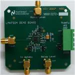
AN-1683 LMH7324 High Speed Comparator Evaluation
Board
1
General Description
This board is designed to demonstrate the LMH7324 quad comparator with RSPECL outputs. It will
facilitate the evaluation of the LMH7324 configured as a window detector. The board detects the level of
the incoming signal and presents the outcome in a 3-bit presentation. One bit indicates that the signal is
below the lowest window level, another bit indicates that the signal is above the highest window level, and
the third bit indicates that the incoming signal is just between both set levels. All three outputs are fed to
SMA connectors mounted at the edge of the board. The impedance of the output track is 50Ω which
makes it easy to connect these signals to any scope or analyzer by the use of a 50Ω coaxial cable. Each
comparator of the LMH7324 has individual positive supplies for the input and output circuits. The negative
supply is common for all input and output circuitry. This setup will work with a supply of ±2.5V as a
minimum supply, with the window voltage centered at ground. If a setup with only one positive supply
voltage is used, jumper J1 (see Figure 7) has to be placed between both positive supply connections. To
examine the possibility of two separate supplies for the input and the output stage the jumper has to be
removed and an extra supply has to be connected.
2
Basic Operation
2.1
Reference Levels
The circuit is built around the four comparators of one LMH7324. Two reference levels are created using
four resisters and two capacitors (R3, R6, R7, R9 and C9, C12 see Figure 7) The ‘ref high’ level is a
positive voltage referred to the ground level and the ‘ref low’ level is a negative voltage referred to ground.
The input connector (con2) is also referenced to ground which means that any AC signal at the input will
vary around the ground level, which is in the center of the reference levels.
2.2
Comparators
The comparators B and C form the window detector, while the comparator A is a level detector indicating
that the input voltage exceeds the ‘ref high’ voltage in the positive direction. The comparator D is a level
detector indicating that the input signal exceeds the ‘ref low’ voltage in the negative direction. The outputs
are connected to a 50Ω connector via a 50Ω track. All three outputs are ‘active low’ as can be seen in
Table 1.
Table 1. Four Comparators Output
VIN
QA
QB
QC
QD
High
0
1
0
1
In Window
1
0
0
1
Low
1
0
1
0
The window detector output is formed by the OR-function of combining both Q outputs of comparators B
and C. Outputs which have an ECL (Emitter Coupled Logic) structure can be wired together to form an
OR function. The overall truth table is shown in Table 2:
SNOA494A – September 2007 – Revised May 2013
Submit Documentation Feedback
AN-1683 LMH7324 High Speed Comparator Evaluation Board
Copyright © 2007–2013, Texas Instruments Incorporated
1
�Layout Considerations
www.ti.com
Table 2. Truth Table
VIN
2.3
Con1
Con3
Con4
High
0
1
1
In Window
1
0
1
Low
1
1
0
Outputs
Every output has a Q and Q connection and both outputs have been made active by a resistor connected
to the VEE terminal. An ECL output becomes active when current flows out of the emitters of the output
stage. This can be done by connecting a resistor to a ‘termination’ voltage (VT) which is 2V below the
VCCO. When using the VT solution every output resistor has to be 50Ω (R1, R2, R4, R5, R10, R11, R12).
Another possibility is to connect a resistor to the most negative supply voltage. In case of a connection to
VEE, the resistor must have a value which causes a current that complies with the ‘Normal Operating’
conditions as mentioned in the datasheet. This demo board is designed for a supply voltage of 5V for the
VCCO with a resistor to VEE with a value of 240Ω (R4 = 360 while R1, R2, R5, R10, R11, R12 = 240). In
case the VCCO is raised to 12V all output resistors to VEE should be replaced with 500Ω resistors except R4
which should be 750Ω. All three output signals are connected via a 50Ω track and a combined capacitor
and jumper which are connected in parallel. A customer can now make a choice between a DC or an AC
coupled output signal. In the case of a DC coupled output be aware of the offset voltage which causes an
extra DC current into a connected scope or analyzer with 50Ω input impedance.
2.4
Supply Voltages
This demo board can operate with a simple dual supply of ±2.5V. The output voltages are now about
1.35V and 1.0V and comply with LVDS and RSPECL levels. In the case of a single supply voltage of +5V
the output levels are 3.85V and 3.5V, which is only RSPECL level compliant. In a single supply
configuration be aware that the detection window starts at VEE level, which is actually the ground level.
The LMH7324 is ground sensing but in this configuration the input signals cannot extend more than 200
mV below the ground level. Every comparator has a separate connection for the VCCI, VCCO and the VEE.
The supply pins are decoupled with a small capacitance of 10 nF to the ground plane. Since the outputs
are referenced to the VCCO the output resistors are decoupled to this supply pin. For better low frequency
decoupling a 47 µF capacitor is placed at the supply connector (con5). The supplies VCCI and VCCO can be
shortened by a jumper (J1) in case both positive supply voltages are the same value.
3
Layout Considerations
The layout is done with a four layer board which makes it easy to keep the design compact with small 50Ω
tracks. The advantage of this is that such tracks route easily and connect perfectly to small components.
At the same time the length and number of supply lines are reduced, while decoupling to these supplies is
easy and direct. Signals are routed on the top and bottom layer, making it easy to measure them.
4
Measurement Hints and Results
Measurements can be done at the output connectors by connecting a scope or analyzer to the test board.
The outputs are capable of driving a 50Ω load. This board offers the possibility of making the output DC or
AC coupled. When DC coupling is used be aware of the DC offset voltage present on the output signals.
When working with a high supply voltage on the VCCO it is possible to damage the output stage of the
device or the input impedance of the equipment. To show what signals can be expected sample
measurement results are shown in the following figures. Measurements were taken at different
frequencies and waveforms. In the first instance measurements were taken at a frequency of 5 MHz with a
sawtooth waveform. The supply voltages are +2.5V and –2.5V. This means that both thresholds are at the
same level of approximately 50 mV. There are three results shown: one with the input signal crossing only
the upper level (see Figure 1) and one while the input signal is only crossing the lowest level (see
Figure 2). The third plot shows the waveforms when the input signal crosses the complete window from
below the lowest level until above the upper level (see Figure 3).
2
AN-1683 LMH7324 High Speed Comparator Evaluation Board
SNOA494A – September 2007 – Revised May 2013
Submit Documentation Feedback
Copyright © 2007–2013, Texas Instruments Incorporated
�Measurement Hints and Results
www.ti.com
input signal
C4
above window
C2
C1
C3
C1 ± 500 mV/DIV
C2 ± 500 mV/DIV
C3 ± 500 mV/DIV
C4 ± 200 mV/DIV
in window
below window
freq C1: 4.921 MHz
freq C4: 4.917 MHz
Timebase: 50 ns/DIV
Trigger: C4
Figure 1. 5 MHz Crossing Upper Level
C4
input signal
above window
C2
C1
C3
C1 ± 500 mV/DIV
C2 ± 500 mV/DIV
C3 ± 500 mV/DIV
C4 ± 200 mV/DIV
in window
below window
freq C1: 4.923 MHz
freq C4: 4.916 MHz
Timebase: 50 ns/DIV
Trigger: C4
Figure 2. 5 MHz Crossing Lower Level
SNOA494A – September 2007 – Revised May 2013
Submit Documentation Feedback
AN-1683 LMH7324 High Speed Comparator Evaluation Board
Copyright © 2007–2013, Texas Instruments Incorporated
3
�Measurement Hints and Results
www.ti.com
input signal
C4
above window
C2
in window
C1
below window
C3
C1 ± 500 mV/DIV
C2 ± 500 mV/DIV
C3 ± 500 mV/DIV
C4 ± 200 mV/DIV
freq C1: 9.485 MHz
freq C4: 4.923 MHz
Timebase: 50 ns/DIV
Trigger: C4
Figure 3. 5 MHz Crossing Whole Window
Higher frequencies will make the pulses much shorter, especially when a sine wave is used and the signal
rises far above the window levels. This situation would make the time that the signal crosses the window
levels very short, because a sine wave has the highest dV/dt at the transition points. Figure 4, Figure 5,
and Figure 6 show the measurements taken when a sine wave is used. In Figure 4 a sine wave of 10 MHz
is used and it just crosses both levels of the window. This creates a reasonable pulse width for both the
detection signals “above window” and “below window” and for the detection signal “in window.” The added
hysteresis works since no oscillations can be seen although the input signal crosses the levels very slowly
and with low overdrive. When using a signal with the same frequency but with a much greater amplitude,
the time it takes for the signal to cross the window becomes much shorter as can be seen in Figure 5.
Note that the frequency of the detection signal “in window” doubles compared to the input frequency. Also
the crossing time through the window levels is very short and, for this example, it is equal to one period of
a frequency of 227 MHz (see marker indication in plot). This means that the detection signal “in window” is
the most critical of the three detection signals and will be the first to incur problems due to frequency
limits. The setup of Figure 6 uses an input frequency of 100 MHz with a big overdrive at the window
levels. This results in a very small pulse for the detection signal “in window” which is equal to one period
of a 1.05 GHz signal (see markers indication in plot). All signals are measured using a cable with a length
of 1 meter connected to a four channel oscilloscope. All channels are AC coupled and terminated with
50Ω.
input signal
C4
above window
C2
in window
C1
below window
C3
C1 ± 500 mV/DIV
C2 ± 500 mV/DIV
C3 ± 500 mV/DIV
C4 ± 200 mV/DIV
freq C1: 20 MHz
freq C4: 10 MHz
Timebase: 50 ns/DIV
Trigger: C4
Figure 4. 10 MHz Just Above Thresholds
4
AN-1683 LMH7324 High Speed Comparator Evaluation Board
SNOA494A – September 2007 – Revised May 2013
Submit Documentation Feedback
Copyright © 2007–2013, Texas Instruments Incorporated
�Measurement Hints and Results
www.ti.com
input
signal
C4
C2
above window in window
C1
below window
C3
C1 ± 500 mV/DIV
C2 ± 500 mV/DIV
C3 ± 500 mV/DIV
C4 ± 200 mV/DIV
freq C1: 20 MHz
freq C4: 10 MHz
'T markers: 4.4 ns
1/'T markers: 227 MHz
Timebase: 50 ns/DIV
Trigger: C4
Figure 5. 10 MHz Far Above Thresholds
input
signal
C4
C2
in window
C1
above window
below window
C3
C1 ± 500 mV/DIV
C2 ± 500 mV/DIV
C3 ± 500 mV/DIV
C4 ± 200 mV/DIV
freq C1: 190.25 MHz
freq C4: 99.98 MHz
'T markers: 950 ps
1/'T markers: 1.05 GHz
Timebase: 5 ns/DIV
Trigger: C4
Figure 6. 100 MHz Far Above Thresholds
SNOA494A – September 2007 – Revised May 2013
Submit Documentation Feedback
AN-1683 LMH7324 High Speed Comparator Evaluation Board
Copyright © 2007–2013, Texas Instruments Incorporated
5
�Board Schematic
5
www.ti.com
Board Schematic
VCCI
VCCO
C2
31 Vcci
30
+
Vee
R2
240
VCCO
10n
47n
Q
9
C4
8
VCCI
10n
C5
R3
10k
11
R6
200
7
Vin
47n
Q
C15
Qn
1
con5
+ C21
47P
25
24
47n
Q
C20
10n
1
0
1
0
2
con3
In Window (active low)
J4
con4
1
22
Below Window (active low)
C24
100n
U1D
LMH7324
- Vcco
+ Vee
23
Vee
GND
1
under ref low
C23
100n
1
27
+ C18
47P
28
2
+ C17
47P
0
VEE
26 Vcci
21
3
C13
10n
J1
jumper if VCCI = VCCO
4
R10
240
U1C
LMH7324
C16
2
0
VEE
VCCI
10n
1
1
VCCO
VCCO
1
in window
2
VEE
Q4
0
18
20
C14
10n
Q3
1
J3
- Vcco
+ Vee
13
R9
10k
Q2
0
19
1
14
Q1
over ref high
VEE
Vee
1
C8
10n
15 Vcci
Ref low
R8
51
VCCI
R5
240
C11
16
C10
con2
Vin
R4
360
VCCO
10n
1
Above Window (active low)
VEE
VCCI
17
R7
200
VEE
Qn
12
10n
C12
10n
window: 200 mV @ VCCI-VEE = 10V
window: 100 mV @ VCCI-VEE = 5V
C22
100n
U1B
LMH7324
- Vcco
+ Vee
5
C7
+
C3
10n
VEE
Vee
C9
10P
R1
240
6
10 Vcci
Ref high
con1
1
Qn
29
4
C6
J2
2
Vee
VCCI
3
U1A
LMH7324
Vcco
2
47n
Q
1
1
10n
32
C1
Qn
R11
240
R12
240
C19
10n
VEE
VEE
VEE
Figure 7. Schematic Diagram
6
AN-1683 LMH7324 High Speed Comparator Evaluation Board
SNOA494A – September 2007 – Revised May 2013
Submit Documentation Feedback
Copyright © 2007–2013, Texas Instruments Incorporated
�Board Layout
www.ti.com
6
Board Layout
Figure 8. Top Side
Figure 9. Bottom Side
SNOA494A – September 2007 – Revised May 2013
Submit Documentation Feedback
AN-1683 LMH7324 High Speed Comparator Evaluation Board
Copyright © 2007–2013, Texas Instruments Incorporated
7
�Board Layout
www.ti.com
Figure 10. Mid Layer 1
Figure 11. Mid Layer 2
8
AN-1683 LMH7324 High Speed Comparator Evaluation Board
SNOA494A – September 2007 – Revised May 2013
Submit Documentation Feedback
Copyright © 2007–2013, Texas Instruments Incorporated
�IMPORTANT NOTICE
Texas Instruments Incorporated and its subsidiaries (TI) reserve the right to make corrections, enhancements, improvements and other
changes to its semiconductor products and services per JESD46, latest issue, and to discontinue any product or service per JESD48, latest
issue. Buyers should obtain the latest relevant information before placing orders and should verify that such information is current and
complete. All semiconductor products (also referred to herein as “components”) are sold subject to TI’s terms and conditions of sale
supplied at the time of order acknowledgment.
TI warrants performance of its components to the specifications applicable at the time of sale, in accordance with the warranty in TI’s terms
and conditions of sale of semiconductor products. Testing and other quality control techniques are used to the extent TI deems necessary
to support this warranty. Except where mandated by applicable law, testing of all parameters of each component is not necessarily
performed.
TI assumes no liability for applications assistance or the design of Buyers’ products. Buyers are responsible for their products and
applications using TI components. To minimize the risks associated with Buyers’ products and applications, Buyers should provide
adequate design and operating safeguards.
TI does not warrant or represent that any license, either express or implied, is granted under any patent right, copyright, mask work right, or
other intellectual property right relating to any combination, machine, or process in which TI components or services are used. Information
published by TI regarding third-party products or services does not constitute a license to use such products or services or a warranty or
endorsement thereof. Use of such information may require a license from a third party under the patents or other intellectual property of the
third party, or a license from TI under the patents or other intellectual property of TI.
Reproduction of significant portions of TI information in TI data books or data sheets is permissible only if reproduction is without alteration
and is accompanied by all associated warranties, conditions, limitations, and notices. TI is not responsible or liable for such altered
documentation. Information of third parties may be subject to additional restrictions.
Resale of TI components or services with statements different from or beyond the parameters stated by TI for that component or service
voids all express and any implied warranties for the associated TI component or service and is an unfair and deceptive business practice.
TI is not responsible or liable for any such statements.
Buyer acknowledges and agrees that it is solely responsible for compliance with all legal, regulatory and safety-related requirements
concerning its products, and any use of TI components in its applications, notwithstanding any applications-related information or support
that may be provided by TI. Buyer represents and agrees that it has all the necessary expertise to create and implement safeguards which
anticipate dangerous consequences of failures, monitor failures and their consequences, lessen the likelihood of failures that might cause
harm and take appropriate remedial actions. Buyer will fully indemnify TI and its representatives against any damages arising out of the use
of any TI components in safety-critical applications.
In some cases, TI components may be promoted specifically to facilitate safety-related applications. With such components, TI’s goal is to
help enable customers to design and create their own end-product solutions that meet applicable functional safety standards and
requirements. Nonetheless, such components are subject to these terms.
No TI components are authorized for use in FDA Class III (or similar life-critical medical equipment) unless authorized officers of the parties
have executed a special agreement specifically governing such use.
Only those TI components which TI has specifically designated as military grade or “enhanced plastic” are designed and intended for use in
military/aerospace applications or environments. Buyer acknowledges and agrees that any military or aerospace use of TI components
which have not been so designated is solely at the Buyer's risk, and that Buyer is solely responsible for compliance with all legal and
regulatory requirements in connection with such use.
TI has specifically designated certain components as meeting ISO/TS16949 requirements, mainly for automotive use. In any case of use of
non-designated products, TI will not be responsible for any failure to meet ISO/TS16949.
Products
Applications
Audio
www.ti.com/audio
Automotive and Transportation
www.ti.com/automotive
Amplifiers
amplifier.ti.com
Communications and Telecom
www.ti.com/communications
Data Converters
dataconverter.ti.com
Computers and Peripherals
www.ti.com/computers
DLP® Products
www.dlp.com
Consumer Electronics
www.ti.com/consumer-apps
DSP
dsp.ti.com
Energy and Lighting
www.ti.com/energy
Clocks and Timers
www.ti.com/clocks
Industrial
www.ti.com/industrial
Interface
interface.ti.com
Medical
www.ti.com/medical
Logic
logic.ti.com
Security
www.ti.com/security
Power Mgmt
power.ti.com
Space, Avionics and Defense
www.ti.com/space-avionics-defense
Microcontrollers
microcontroller.ti.com
Video and Imaging
www.ti.com/video
RFID
www.ti-rfid.com
OMAP Applications Processors
www.ti.com/omap
TI E2E Community
e2e.ti.com
Wireless Connectivity
www.ti.com/wirelessconnectivity
Mailing Address: Texas Instruments, Post Office Box 655303, Dallas, Texas 75265
Copyright © 2013, Texas Instruments Incorporated
�