User's Guide
SNLU098A – March 2012 – Revised July 2019
LMK00101 User’s Guide
This user guide describes how to set up and operate the LMK00101 evaluation board kit (EVK). The
LMK00101 is a high performance, low noise, low voltage CMOS fanout buffer. The core voltage can be
2.5 or 3.3 volts, while the power supply for the outputs can be selected from: 1.5 V, 1.8 V, 2.5 V, or 3.3 V,
provided that it does not exceed the core supply voltage .
1
2
3
4
5
6
7
8
9
Contents
Introduction ...................................................................................................................
Quick Start ....................................................................................................................
2.1
Quick Start Description.............................................................................................
Signal Path and Control Switches .........................................................................................
Power Supplies ..............................................................................................................
Clock Inputs ..................................................................................................................
5.1
Crystal Oscillator Interface.........................................................................................
5.2
Configuring OSCin for a Crystal Mode ...........................................................................
Clock Outputs ................................................................................................................
Schematics ...................................................................................................................
PCB Layout ...................................................................................................................
Bill of Materials ...............................................................................................................
2
2
3
3
4
4
4
4
4
5
7
9
List of Figures
1
LMK00101 Quick Start Setup .............................................................................................. 2
2
Schematic Sheet 1
5
3
Schematic Sheet 2
6
4
5
..........................................................................................................
..........................................................................................................
PCB Top ......................................................................................................................
Bottom Side (Layer Inverted, Not to Scale) ..............................................................................
7
8
List of Tables
1
Part Description .............................................................................................................. 2
2
Default Clock Output Modes / Interfaces ................................................................................. 3
3
Input Selection (0=SW OFF, 1=SW ON) ................................................................................. 3
4
Output Enable Selection (0=OFF, 1=ON) ................................................................................ 3
5
Power Supply Configuration ................................................................................................ 4
6
Bill of Materials ............................................................................................................... 9
Trademarks
All trademarks are the property of their respective owners.
SNLU098A – March 2012 – Revised July 2019
Submit Documentation Feedback
LMK00101 User’s Guide
Copyright © 2012–2019, Texas Instruments Incorporated
1
�Introduction
1
www.ti.com
Introduction
This user guide describes how to set up and operate the LMK00101 evaluation board kit (EVK). The
LMK00101 is a high performance, low noise, low voltage CMOS fanout buffer. The core voltage can be
2.5 or 3.3 volts, while the power supply for the outputs can be selected from: 1.5 V, 1.8 V, 2.5 V, or 3.3 V,
provided that it does not exceed the core supply voltage .
Table 1. Part Description
2
BUFFER
IC
PACKAGE
U1
LMK00101
LLP-32
Quick Start
Output
Power Supply
Core
Power Supply
Differential
CLKin1
Input Select
DIP Switches
CLKout0CLKout5
CLKout6CLKout9
Single Ended
Oscillator Input
Differential
CLKin0
Figure 1. LMK00101 Quick Start Setup
2
LMK00101 User’s Guide
SNLU098A – March 2012 – Revised July 2019
Submit Documentation Feedback
Copyright © 2012–2019, Texas Instruments Incorporated
�Quick Start
www.ti.com
2.1
Quick Start Description
The LMK00101 EVK allows full verification of the device functionality and performance specifications. To
quickly set up and operate the board with basic equipment, refer to the quick start procedure below and
test setup shown in Figure 1.
1. Verify the output mode control switches, S1[1:4], match the states shown in Table 2 to reflect the
default output clock interfaces configured on the EVK.
Table 2. Default Clock Output Modes / Interfaces
SW POSITION/NAME
SW STATE
S1[1] / SEL1
0 (OFF)
S1[2] / SEL0
1 (ON)
S1[3] / OE
1 (OFF)
S1[4] / NC
Unused
2. Connect the Vdd SMA from the board to a 3.3 V source. This powers the non-output portions of the
LMK00101.
3. Connect the Vdd CLKout SMA from the board to a 3.3 V source. This powers the output drivers of the
LMK00101.
4. Set the desired clock input using the input selection control switches, S1[1:2], per Table 3. A
differential clock source can be connected to SMAs CLKin0/0* or CLKin1/1*.
Note: CLKin0/0* and CLKin1/1* paths are configured by default to receive a differential clock as the
input. The SMA inputs are DC coupled to the device inputs and terminated with 100 Ω differential.
Refer to the Clock Inputs section to configure the EVK for a single-ended input.
Table 3. Input Selection (0=SW OFF, 1=SW ON)
SELECTED INPUT
DEFAULT INPUT MODE
S1[1]CLKin_Sel0 State
S1[2] CLKin_Sel1 State
CLKin0/0*
Differential clock
0
0
CLKin1/1*
Differential clock
0
1
OSCin
Select OSCin
1
Don't Care
5. Connect and measure any clock output SMA labeled CLKoutX to an oscilloscope or other test
instrument using SMA cable(s). The output clock will be level-translated/buffered copy of the selected
clock input or crystal oscillator. Note: All output clocks are AC-coupled to the SMA connectors to
ensure safe use with RF instruments.
Note: Switching noise from one or more un-terminated outputs may impair the signal quality of the
measured output(s). To minimize switching noise and EMI, properly terminate any unused output path
using an SMA load or the component options near the SMA outputs, or alternatively, remove the 0 Ω
series resistor nearest the unused output pin.
3
Signal Path and Control Switches
The LMK00101 supports single-ended or differential clocks on CLKin0 and CLKin1. A third input, OSCin,
has an integrated crystal oscillator interface that supports a fundamental mode, AT-cut crystal or an
external single-ended clock. The three-input multiplexer is pin-controlled. To achieve the maximum
operating frequency and lowest additive jitter, it is recommended to use a differential clock with high input
slew rate (>1 V/ns) and DC-coupling to either CLKin0 or CLKin1 port.
All control pins are configured with the control switch, S3. The output enable logic is shown in Table 4.
Table 4. Output Enable Selection (0=OFF, 1=ON)
CLKout ENABLE MODE
S1[3]-OE
Disabled/Hi-Z
0
Enabled
1
SNLU098A – March 2012 – Revised July 2019
Submit Documentation Feedback
LMK00101 User’s Guide
Copyright © 2012–2019, Texas Instruments Incorporated
3
�Power Supplies
4
www.ti.com
Power Supplies
By default, Vdd and VddCLKout are supplied by two external power supplies. To modify the EVK with a
different power supply configuration, populate the resistor options as shown in Table 5.Then, apply the
appropriate voltage(s) to the EVK power input(s).
Decoupling capacitors and 0 Ω resistor footprints, which can accommodate ferrite beads, can be used to
isolate the EVK power input(s) from the device power pins. Do not disconnect or ground any of the
VddCLKout pins as they are all internally connected inside the device.
Table 5. Power Supply Configuration
5
DUAL EXTERNAL INPUTS (DEFAULT)
SINGLE EXTERNAL INPUT 3.3 V
Vdd input
Apply 3.3 V
Apply 3.3 V ± 5%
VddCLKout input
Apply Voltage ≤Vdd
Not used
R38
0Ω
DNP
R39
0Ω
0Ω
R43
DNP
0Ω
Clock Inputs
The SMA inputs labeled CLKin0 & CLKin0* and CLKin1 & CLKin1* are configured to receive a differential
clock or single ended clock. Best performance is achieved with DC-coupled differential input clock.
5.1
Crystal Oscillator Interface
The LMK00101 has an integrated crystal oscillator interface (OSCin/OSCout) that supports a fundamental
mode, AT-cut crystal. If the crystal input is selected, an optional onboard crystal on either footprint Y1 or
Y2 will start-up and the oscillator clock can be measured on any enabled output.
A crystal with the HC49 footprint can be populated on the bottom side of the PCB. Alternatively, a 3.2 x
2.5 mm crystal can be populated on Y2, located on the top side. Only one crystal footprint should be used
at a time.
The values of C42 and C25(CEXT) depend on the load capacitance (CL) specified for the crystal. The OSC
input capacitance (CIN) of the device is 1 pF differential, and the trace capacitance (CTRACE) of OSCin and
OSCout is around 1 pF. If the selected crystal is specified for CL of 18 pF, the CEXT is calculated as
follows:
CEXT= (CL–CIN–CTRACE/2) * 2
CEXT= (18 pF –1 pF –1 pF/2) * 2
CEXT= 33 pF
5.2
(1)
(2)
(3)
Configuring OSCin for a Crystal Mode
To configure the board to use crystal mode remove C26 to disconnect the OSCin Port. Install 0 Ω resistors
on R33 and R34. Install a crystal in either footprint (Y1 or Y2) and install the proper load capacitors in C24
and C25.
6
Clock Outputs
All clock outputs are LVCMOS. In the case that not all outputs are used, any unused outputs should be
left floating.
4
LMK00101 User’s Guide
SNLU098A – March 2012 – Revised July 2019
Submit Documentation Feedback
Copyright © 2012–2019, Texas Instruments Incorporated
�D
C
B
1
CLKin1*
1
C1
10μF
GND
GND
VCC
GND
1
3
5
7
9
8
7
6
5
HEADER_2X5
DNP
uWire
2
4
6
8
10
GND
142-0701-851
R1
DNP
100
C3
0.01μF
GND
CLKin1
1
C2
1μF
VCC
A6S-4104-H
1 S1
2
3
4
142-0701-851
2
3
4
5
R37
R36
R35
R300
DNP
4.7k
R301
DNP
4.7k
R302
DNP
4.7k
0
0
0
R2
DNP
100
C1in_N
0.1uF
R5
100
CLKout0
1
CLKout1
1
GND
142-0701-851
GND
2
142-0701-851
GND
GND
R19
DNP
51
GND
R18
DNP
51
0.1μF
C28
GND
0.1μF
DNP
C19
0.1μF
C27
0
R32
VCCO
GND
33
32
31
OE
29
30
SEL1
28
27
26
25
GND
DNPC18
0.01μF
DAP
GND
OE
SEL0
SEL1
CLKin1
CLKin1*
GND`
GND
GND
C41
100pF
GND
DNPC11
0.01μF
SEL0
C1_P
0
C21
GND
GND
C1_N
R303
R304 R305
DNP
15k DNP
15k DNP
15k
R28
0
DNPC10
0.1μF
VCCO
0.1μF
C36
0
C20
GND
R27
DNP
51
R6 R7
DNP
51DNP
51
C1in_PR4
0.1uF
142-0701-851
GND
R3
142-0701-851
R26
DNP
51
0.1μF
C35
22
GND
C37
100pF
3
3
GND
U1
LMK00101
GND
18
GND
R25
DNP
51
GND
0.1μF
C29
C38
100pF
0.1μF
C34
19
2
23
GND
0.1μF
C30
GND
Vdd
OSCin
OSCout
CLKin0
CLKin0*
GND
GND
GND
R20
DNP
51
R29
VCCO
GND
R24
DNP
51
CLKout7
1
GND
R21
DNP
51
0
R31
CLKout2
1
GND
R22
DNP
51
VCCO
DNPC16
0.1μF
0
GND
0
R17
GND
0
R16
51
5.6pF
DNP
C25
C24 5.6pF
DNP
R15
Y1
Y2
DNP 40 MHzDNP
R9
DNP
100
CLKin0
C0_P 1
4
GND
142-0701-851
GND
CLKin0*
1
GND
142-0701-851
142-0701-851
OSCin
1
GND
R8
DNP
100
C0_N
5
Designed for: Public Release
Mod. Date: 3/20/2012
Project: LMK00101 EVK
Sheet Title: LMK00101 Main Schematic
Sheet:1 of 2
Size: B
Rev: X1
Schematic: 870600680
Assembly Variant: Customer
File: LMK0101ENG_Sheet2.SchDoc
Contact: http://www.national.com/support
Note: Parts with Designators greater than or equal to 300 are on the bottom side.
GND
142-0701-851
GND
0.1μF
142-0701-851
CLKout3
1
142-0701-851
R33
DNP
0
C26
0.1uF
R11
0.1uF
R10
R13 R12
DNP
51DNP
51
R34
DNP
0
R14
100
GND
142-0701-851
GND
142-0701-851
CLKout5
1
CLKout4
1
C23
GND
0.1μF
DNP
VCC
C14
0
CLKout6
1
5
Texas Instruments and/or its licensors do not warrant the accur acy or completeness of this
specification or any information contained therein. Texas Instruments and/or its licensors do not
warrant that this design will meet the specifications, will be suitable for your application or fit for
any particular purpose, or will operate in an implementation. Texas Instruments and/or its
licensors do not warrant that the design is production worthy. You should completely validate
and test your design implementation to confirm the system funct ionality for your application.
0.1μF
R30
C0in_P
C0in_N
0
C39
DNPC15
0.01μF 100pF
GND
DNPC17
0.01μF
C31
9
10
11
12
13
14
15
16
GND
C22
R23
DNP
51
GND
142-0701-851
0
C40 DNPC12
DNPC13
100pF
0.01μF
0.1μF
GND
0.1μF
C32
0.1μF
C33
4
5
4
3
2
CLKout8
1
CLKout9
GND
1
2
3
4
5
A
2
3
4
5
24
CLKout9
CLKout0
1
VddCLKout
VddCLKout
2
21
GND
4
CLKout8
CLKout1
3
GND
20
CLKout7
CLKout2
5
VddCLKout
VddCLKout
6
CLKout6
17
CLKout5
CLKout3
7
CLKout4
8
5
4
3
2
2
3
4
5
2
3
4
5
Copyright © 2012–2019, Texas Instruments Incorporated
5
4
3
2
SNLU098A – March 2012 – Revised July 2019
Submit Documentation Feedback
5
4
3
2
5
4
3
2
5
4
3
2
5
4
3
2
5
4
3
2
5
4
3
2
6
6
http://www.ti.com
© Texas Instruments 2011
D
C
B
A
7
2
3
4
5
1
www.ti.com
Schematics
Schematics
Figure 2. Schematic Sheet 1
LMK00101 User’s Guide
5
�LMK00101 User’s Guide
Copyright © 2012–2019, Texas Instruments Incorporated
D
C
B
1
VddCLKout
1
Vdd
1
GND
142-0701-851
GND
TERMBLOCK_2
1
1
DNP2
2
Vdd_TB
2
VccIN
142-0701-851
GND
2
GND
TERMBLOCK_2
VddCLKout_TB
1
1
DNP2
2
2
3
4
5
6
2
3
4
5
A
1
0
R38
R41
DNP
0
R40
DNP
0
TPVccIN
DNP
0
R39
GND
DNPC304
10μF
GND
DNPC300
10μF
GND
C4
10μF
R310
DNP
51k
R306
DNP
51k
C5
1μF
C7
10μF
2
7
9
8
4
OUT
3
1
6
5
2
7
9
8
4
OUT
GND
TPVcco
DNP
TPVcc
DNPC303
0.01μF
DNP
3
GND
3
TP_VCCO_LDO
DNP
TP_VCC_LDO
DNP
R43
DNP
0
4
SO5
SO2
SO1
0.375" Standoff
0.375" Standoff
0.375" Standoff
0.375" Standoff
SO3
0.375" Standoff
0.375" Standoff
SO6
SO4
PCB Part Number: 551600680 - 001 REV A
5
4
5
Designed for: Public Release
Mod. Date: 3/20/2012
Texas Instruments and/or its licensors do not warrant the accur acy or completeness of this
Project: LMK00101 EVK
specification or any information contained therein. Texas Instr uments and/or its licensors do not
Sheet Title: LMK00101 Power Supply
Sheet:2 of 2
warrant that this design will meet the specifications, will be suitable for your application or fit for
Size: B
Rev: X1
Schematic: 870600680
any particular purpose, or will operate in an implementation. Texas Instruments and/or its
Assembly Variant: Customer
licensors do not warrant that the design is production worthy. You should completely validate
File: LMK0101ENG_Sheet3.SchDoc
and test your design implementation to confirm the system funct ionality for your application.
Contact: http://www.national.com/support
C305
R312
DNP
DNP
2.00k DNPC306
2200pF
10μF
R42
DNP
0
R307
DNP
866
C301
R308
DNP
DNP
1.30k DNPC302
2200pF
10μF
R309
DNP
0
DNPC307
0.01μF
R311
DNP
866
LP3878SD-ADJ/NOPB
1
6
5
C9
0.01μF
ADJ
DNP
NC
BYP
NC
DAP GND
SD
IN
U3
C8
1μF
VCC
GND
LP3878SD-ADJ/NOPB
ADJ
DNP
NC
BYP
NC
DAP GND
SD
IN
U2
C6
0.1μF
VCCO
3
6
6
http://www.ti.com
© Texas Instruments 2011
D
C
B
A
Schematics
www.ti.com
Figure 3. Schematic Sheet 2
SNLU098A – March 2012 – Revised July 2019
Submit Documentation Feedback
�PCB Layout
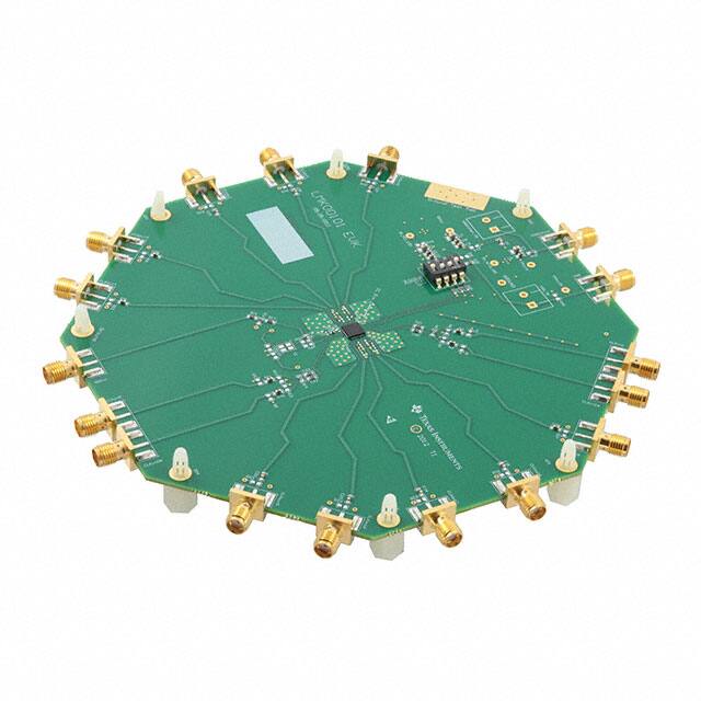
www.ti.com
8
PCB Layout
Figure 4. PCB Top
SNLU098A – March 2012 – Revised July 2019
Submit Documentation Feedback
LMK00101 User’s Guide
Copyright © 2012–2019, Texas Instruments Incorporated
7
�PCB Layout
www.ti.com
Figure 5. Bottom Side (Layer Inverted, Not to Scale)
8
LMK00101 User’s Guide
SNLU098A – March 2012 – Revised July 2019
Submit Documentation Feedback
Copyright © 2012–2019, Texas Instruments Incorporated
�Bill of Materials
www.ti.com
9
Bill of Materials
Table 6. Bill of Materials
Item
DESCRIPTION
QTY
DESIGNATOR
MANUFACTURER
PART NUMBER
1
CAP, CERM, 10uF, 10V,
+/-10%, X5R, 0805
3
C1, C4, C7
MuRata
GRM21BR61A106KE19L
2
CAP, CERM, 1uF, 16V, +/10%, X7R, 0603
3
C2, C5, C8
TDK
C1608X7R1C105K
3
CAP, CERM, 0.01uF,
100V, +/-5%, X7R, 0603
2
C3, C9
Kemet
C0603C103J1RACTU
4
CAP, CERM, 0.1uF, 16V,
+80/-20%, Y5V, 0603
1
C6
TDK
C1608Y5V1C104Z
5
RES, 0 ohm, 5%, 0.1W,
0603
11
C20, C21, C22, C23, R15,
R17, R35, R36, R37, R38,
R39
Vishay-Dale
CRCW06030000Z0EA
6
CAP, CERM, 0.1uF, 16V,
+/-10%, X7R, 0603
15
C26, C27, C28, C29, C30,
C31, C32, C33, C34, C35,
C36, R3, R4, R10, R11
TDK
C1608X7R1C104K
7
CAP, CERM, 100pF, 25V,
+/-5%, C0G/NP0, 0402
5
C37, C38, C39, C40, C41
MuRata
GRM1555C1E101JA01D
Emerson Network Power
Connectivity
142-0701-851
8
Connector, SMT, End
launch SMA 50 ohm
17
CLKin0, CLKin0*, CLKin1,
CLKin1*, CLKout0,
CLKout1, CLKout2,
CLKout3, CLKout4,
CLKout5, CLKout6,
CLKout7, CLKout8,
CLKout9, OSCin, Vdd,
VddCLKout
9
RES, 100 ohm, 5%, 0.1W,
0603
2
R5, R14
Vishay-Dale
CRCW0603100RJNEA
10
RES, 51 ohm, 5%, 0.1W,
0603
1
R16
Vishay-Dale
CRCW060351R0JNEA
11
RES, 0 ohm, 5%, 0.063W,
0402
5
R28, R29, R30, R31, R32
Vishay-Dale
CRCW04020000Z0ED
12
DIP Switch, 4 position slide
1
actuator, SPST, SMD
S1
Omron Electronic
Components
A6S-4104-H
13
0.375" Standoff
6
SO1, SO2, SO3, SO4,
SO5, SO6
14
LMK00101
1
U1
Texas Instruments
LMK00101
15
CAP, CERM, 0.1uF, 16V,
+80/-20%, Y5V, 0402
0
C10, C13, C14, C16, C19
TDK
C1005Y5V1C104Z
16
CAP, CERM, 0.01uF, 25V,
+/-10%, X7R, 0402
0
C11, C12, C15, C17, C18
TDK
C1005X7R1E103K
17
CAP, CERM, 5.6pF, 50V,
+/-5%, C0G/NP0, 0603
0
C24, C25
AVX
06035A5R6CAT2A
18
CAP, CERM, 10uF, 10V,
+/-10%, X5R, 0805
0
C300, C302, C304, C306
MuRata
GRM21BR61A106KE19L
19
CAP, CERM, 2200pF,
100V, +/-5%, X7R, 0603
0
C301, C305
AVX
06031C222JAT2A
20
CAP, CERM, 0.01uF, 25V,
+/-5%, C0G/NP0, 0603
0
C303, C307
TDK
C1608C0G1E103J
21
RES, 100 ohm, 5%, 0.1W,
0603
0
R1, R2, R8, R9
Vishay-Dale
CRCW0603100RJNEA
22
RES, 51 ohm, 5%, 0.1W,
0603
0
R6, R7, R12, R13, R18,
R19, R20, R21, R22, R23,
R24, R25, R26, R27
Vishay-Dale
CRCW060351R0JNEA
23
RES, 0 ohm, 5%, 0.1W,
0603
0
R33, R34, R40, R41, R42,
R43, R309
Vishay-Dale
CRCW06030000Z0EA
24
RES, 4.7k ohm, 5%, 0.1W,
0603
0
R300, R301, R302
Vishay-Dale
CRCW06034K70JNEA
SNLU098A – March 2012 – Revised July 2019
Submit Documentation Feedback
LMK00101 User’s Guide
Copyright © 2012–2019, Texas Instruments Incorporated
9
�Bill of Materials
www.ti.com
Table 6. Bill of Materials (continued)
Item
DESCRIPTION
25
RES, 15k ohm, 5%, 0.1W,
0603
0
R303, R304, R305
Vishay-Dale
CRCW060315K0JNEA
26
RES, 51k ohm, 5%, 0.1W,
0603
0
R306, R310
Vishay-Dale
CRCW060351K0JNEA
27
RES, 866 ohm, 1%, 0.1W,
0603
0
R307, R311
Vishay-Dale
CRCW0603866RFKEA
28
RES,1.30k ohm, 1%, 0.1W,
0
0603
R308
Vishay-Dale
CRCW06031K30FKEA
29
RES, 2.00k ohm, 1%,
0.1W, 0603
0
R312
Vishay-Dale
CRCW06032K00FKEA
30
Testpoint
0
TP_VCC_LDO,
TP_VCCO_LDO, TPVcc,
TPVccIN, TPVcco
31
Micropower800mA Low
Noise "Ceramic Stable"
Adjustable Voltage
Regulator for 1V to 5V
Applications, 8-pin LLP,
Pb-Free
0
U2, U3
Texas Instruments
LP3878SD-ADJ/NOPB
0
uWire, Vdd_TB,
VddCLKout_TB
32
10
QTY
DESIGNATOR
33
Crystal, xxxMHz, xxpF,
[MountType]
0
Y1
34
Crystal, Citizen CS325,
XXMHz
0
Y2
MANUFACTURER
LMK00101 User’s Guide
PART NUMBER
SNLU098A – March 2012 – Revised July 2019
Submit Documentation Feedback
Copyright © 2012–2019, Texas Instruments Incorporated
�Revision History
www.ti.com
Revision History
NOTE: Page numbers for previous revisions may differ from page numbers in the current version.
Changes from Original (March 2012) to A Revision ....................................................................................................... Page
•
Changed document throughout. ......................................................................................................... 2
SNLU098A – March 2012 – Revised July 2019
Submit Documentation Feedback
Revision History
Copyright © 2012–2019, Texas Instruments Incorporated
11
�IMPORTANT NOTICE AND DISCLAIMER
TI PROVIDES TECHNICAL AND RELIABILITY DATA (INCLUDING DATA SHEETS), DESIGN RESOURCES (INCLUDING REFERENCE
DESIGNS), APPLICATION OR OTHER DESIGN ADVICE, WEB TOOLS, SAFETY INFORMATION, AND OTHER RESOURCES “AS IS”
AND WITH ALL FAULTS, AND DISCLAIMS ALL WARRANTIES, EXPRESS AND IMPLIED, INCLUDING WITHOUT LIMITATION ANY
IMPLIED WARRANTIES OF MERCHANTABILITY, FITNESS FOR A PARTICULAR PURPOSE OR NON-INFRINGEMENT OF THIRD
PARTY INTELLECTUAL PROPERTY RIGHTS.
These resources are intended for skilled developers designing with TI products. You are solely responsible for (1) selecting the appropriate
TI products for your application, (2) designing, validating and testing your application, and (3) ensuring your application meets applicable
standards, and any other safety, security, regulatory or other requirements.
These resources are subject to change without notice. TI grants you permission to use these resources only for development of an
application that uses the TI products described in the resource. Other reproduction and display of these resources is prohibited. No license
is granted to any other TI intellectual property right or to any third party intellectual property right. TI disclaims responsibility for, and you
will fully indemnify TI and its representatives against, any claims, damages, costs, losses, and liabilities arising out of your use of these
resources.
TI’s products are provided subject to TI’s Terms of Sale or other applicable terms available either on ti.com or provided in conjunction with
such TI products. TI’s provision of these resources does not expand or otherwise alter TI’s applicable warranties or warranty disclaimers for
TI products.
TI objects to and rejects any additional or different terms you may have proposed. IMPORTANT NOTICE
Mailing Address: Texas Instruments, Post Office Box 655303, Dallas, Texas 75265
Copyright © 2022, Texas Instruments Incorporated
�


 工商网监
湘ICP备2023018690号
工商网监
湘ICP备2023018690号