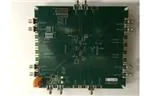
LMK00338EVM
User's Guide
Literature Number: SNAU155
November 2013
�User's Guide
SNAU155 – November 2013
LMK00338EVM User Guide
This user guide describes how to set up and operate the LMK00338 evaluation module (EVM). The
LMK00338 is a 400 MHz, 8-output HCSL clock buffer intended for high frequency, low additive jitter clock
distribution and level translation. The EVM allows the user to verify the functionality and performance
specifications of the device. Refer to the LMK00338 datasheet for the functional description and
specifications.
Topic
1
2
3
4
5
6
7
8
9
10
11
...........................................................................................................................
Page
General Description ............................................................................................ 3
Features ............................................................................................................. 3
Quick Setup ....................................................................................................... 3
Signal Path and Control Switches ......................................................................... 4
Power Supplies ................................................................................................... 5
Clock Inputs ....................................................................................................... 6
Crystal Oscillator Interface ................................................................................... 7
Clock Outputs .................................................................................................... 7
Schematics ........................................................................................................ 8
Board Layout .................................................................................................... 11
Bill of Materials ................................................................................................. 13
All trademarks are the property of their respective owners.
2
LMK00338EVM User Guide
SNAU155 – November 2013
Submit Documentation Feedback
Copyright © 2013, Texas Instruments Incorporated
�General Description
www.ti.com
1
General Description
2
Features
•
•
•
•
•
3
Low-noise clock fan-out via two banks of four HCSL outputs and one LVCMOS output
3:1 input multiplexer with two universal input buffers and one crystal oscillator interface
DIP switch control of device configuration
3.3 V core and 3 independent 3.3 V/2.5 V output supplies (one per output bank) using external supply
inputs or optional LP3878-ADJ LDO or LMZ10500 switching regulator on board
AC- or DC-coupled input & output interface with low-skew, controlled-impedance traces and edge SMA
connectors
Quick Setup
O-SCOPE
(50Ω inputs)
50Ω TERM
REFout
(LVCMOS)
To quickly set up and operate the board with basic equipment, refer to the setup procedure below and test
setup shown in Figure 1.
LMK0033x
EVALUATION
MODULE
CLKinX
Bank A Outputs
(DC Coupled HCSL)
CLOCK
SOURCE
(OPTIONAL)
CLKoutBn
CLKoutBn*
CLKinX*
CLKoutAn
CLKoutAn*
VCC_EXT
4 to 6 V
GND
GND
POWER
SUPPLY
50Ω TERM
50Ω TERM
Bank B Outputs
(DC Coupled HCSL)
Bottom side:
25 MHz Crystal
(Default Input)
Note: Terminate unused
output traces (or disconnect
from output pin on PCB)
Figure 1. LMK00338 Evaluation Board Quick Start Setup
SNAU155 – November 2013
Submit Documentation Feedback
LMK00338EVM User Guide
Copyright © 2013, Texas Instruments Incorporated
3
�Signal Path and Control Switches
www.ti.com
Setup Procedure:
1. Verify the output mode control switches, S1[1:5], match the states shown in Table 1 to reflect the
default output clock interfaces configured on the EVM.
Table 1. Default Clock Output Modes
SW Position/Name
SW State
Default Clock Output Modes
S1[2] / CLKoutB_A_EN
OFF
Bank A outputs enabled
S1[4] / CLKoutB_B_EN
OFF
Bank B outputs enabled
S1[5] / REFout_EN
ON
REFout (CMOS) enabled
2. Connect a 4 to 6 V power supply to VCC_EXT and GND terminals of the power block labeled J2. This
powers the on-board LDO regulator to supply 3.3 V to the VCC and VCCO rails of the IC. Both VCC &
VCCO status LEDs should be lit green when ON.
3. Set the desired clock input using the input selection control switches, S1[6:7], as seen in Table 2. The
onboard 25 MHz crystal (Y1) can be selected, so an external clock source is not required. A differential
clock source can be connected to SMAs labeled CLKin0/0* or CLKin1/1*. By default, these differential
inputs are AC coupled and terminated near the device with 100 Ω differential. To configure the EVM for
a single-ended input, refer to the Clock Inputs section.
Table 2. Input Selection
Selected Input
Default Input Mode
S1[6] CLKin_Sel1 State
S1[7] CLKin_Sel0 State
CLKin0/0*
Differential clock
OFF
OFF
CLKin1/1*
Differential clock
OFF
ON
OSCin
25 MHz XTAL onboard
ON
Don't care
4. Connect and measure any clock output SMA labeled CLKoutA#/A#*, CLKoutB#/B#*, or REFout to an
oscilloscope or other test instrument using SMA cable(s). The output clock will be a leveltranslated/buffered copy of the selected clock input or crystal oscillator. Note: All output clocks are DCcoupled to the SMA connectors.
Note: Any active output trace(s) without proper load termination can cause signal reflections on the
board, which can couple onto nearby outputs and degrade signal quality and measurement accuracy.
To minimize these effects, be sure to properly terminate any unused output trace with a 50 Ω SMA
load, or else disconnect any unused output trace from the device output pin by removing the series 0 Ω
resistor. An unused output or output bank may also be disabled using the output mode control switch.
4
Signal Path and Control Switches
The LMK00338 supports single-ended or differential clocks on CLKin0 and CLKin1. A third input, OSCin,
has an integrated crystal oscillator interface that supports a fundamental mode, AT-cut crystal or an
external single-ended clock. To achieve the maximum operating frequency and lowest additive jitter, it is
recommended to use a differential input clock with high slew rate (>3 V/ns) on either CLKin0 or CLKin1
port.
The device provides up to 8 HCSL outputs with pin-selectable output enable (HCSL, or Hi-Z). An
additional output, REFout, has a fixed LVCMOS buffer with output enable input.
All control pins are configured with the control DIP switch, S1. The input selection logic is shown in
Table 2. The output enable selection logic for Bank A and Bank B are shown in Table 1. The REFout
enable logic is shown in Table 3.
Table 3. REF out Enable Selection
4
REFout Enable Mode
S1[5] REFout_EN State
Disabled/Hi-Z
OFF
Enabled
ON
LMK00338EVM User Guide
SNAU155 – November 2013
Submit Documentation Feedback
Copyright © 2013, Texas Instruments Incorporated
�Power Supplies
www.ti.com
5
Power Supplies
The power supply section on the EVM provides flexibility to power the device using the onboard
regulator(s) or direct supply input(s). A combination of 0 Ω resistor options allows the user to modify the
EVM power supply configuration, if desired.
By default, 3.3 V is supplied to both VCC and VCCO rails by the onboard LDO regulator, U3. To power
the regulator, connect a 4 V to 6 V input voltage and ground from an external power source to the terminal
block, J2, or SMA input labeled VCC_EXT.
To modify the EVM with a different power supply configuration, populate the resistor options as shown in
Table 4. Then, apply the appropriate voltage(s) to the EVM power input(s).
If the EVM is configured for dual direct supplies, connect the 3.3 V supply and ground to VCC_EXT and
the 2.5 V supply and ground to the SMA input labeled VCCO_EXT.
Decoupling capacitors and 0 Ω resistor footprints, which can accommodate ferrite beads, can be used to
isolate the EVM power input(s) from the device power pins.
Table 4. EVM Power Supply Configuration Options
5.1
LP3878 LDO
Regulator (U3)
3.3 V (DEFAULT)
LMZ10500
Switcher (U2)
3.3 V
Single
Direct Supply
3.3 V
Dual
Direct Supplies
3.3 V & 2.5 V
VCC_EXT port
(J2 or SMA)
Apply 4 V to 6 V
Apply 4 V to 5.5 V
Apply 3.3 V ± 5%
Apply 3.3 V ± 5%
VCCO_EXT port
(SMA)
Not used
Not used
Not used
Apply 2.5 V ± 5%
U2 Vout
Not used
3.3 V (VCC & VCCO)
Not used
Not used
U3 Vout
3.3 V (VCC & VCCO)
Not used
Not used
Not used
R131
OPEN
OPEN
OPEN
0
R132
0
0
0
0
R134
OPEN
0
OPEN
OPEN
R145
OPEN
0
OPEN
OPEN
R153
OPEN
OPEN
0
0
R155
0
OPEN
OPEN
OPEN
R156
0
OPEN
OPEN
OPEN
Independent Output Supply Voltages
On the bottom side of the EVM, resistor options provide flexibility to power each of the three individual
output supply pins (VCCOA, VCCOB, and VCCOC) from either VCC or VCCO rail. This is useful when 3.3
V and 2.5 V are both needed for separate output supplies.
The EVM power supply needs to be modified to get 2.5 V on the VCCO rail, either using the VCCO_EXT
input or LMZ10500 switcher, as seen in Table 4. To configure LMZ10500 with 2.5 V output, set R138 to
150k and R139 to 118k.
Note: When the LMZ10500 switcher is used to power the DUT and an ultra-low-noise clock source is
used, the higher output noise voltage of the switcher (compared to the LP3878-ADJ) can cause an slight
increase in the output phase noise floor at low offset frequencies as well as low-level spurs. The high
PSRR of the device helps to minimize supply-induced jitter.
SNAU155 – November 2013
Submit Documentation Feedback
LMK00338EVM User Guide
Copyright © 2013, Texas Instruments Incorporated
5
�Clock Inputs
6
www.ti.com
Clock Inputs
The SMA inputs labeled CLKin0 & CLKin0* and CLKin1 & CLKin1* can be configured to receive a
differential clock or single-ended clock. Best performance is achieved with a differential input clock, which
is the default configuration for both CLKin ports.
Both CLKin0 and CLKin1 paths include footprint options to provide the user with flexibility in configuring
the termination, biasing, and coupling for the device inputs.
6.1
Configuring CLKinX+ for a Single Ended Input
To configure an AC-coupled or DC-coupled single-ended clock input on CLKin0, follow the steps below.
CLKin1 can be modified similarly.
1. Remove R24 (100 Ω differential termination).
2. Terminate CLKin0 (driven input) by installing 51 Ω on R30.
3. Install 0.1 uF on C10 as a bypass capacitor.
4. Modify for AC or DC coupled input:
(a) AC-coupled input: Install 0 Ω on R23, so CLKin0* input pin is AC coupled to ground via C17.
(b) DC-coupled input:
(i) Replace R22 and R28 with 0 Ω to DC couple the input path.
(ii) Bias CLKin0*(non-driven input) with a reference voltage near the common-mode voltage of the
DC-coupled input signal (on CLKin0) using R21 and R23 to form a voltage divider from VCC.
For example, if CLKin0 will be driven by a single-ended, DC-coupled LVCMOS signal with a commonmode voltage of 1.65 V, then 1 kΩ resistors can be installed on R21 and R23 to bias CLKin0* to VCC/2.
6
LMK00338EVM User Guide
SNAU155 – November 2013
Submit Documentation Feedback
Copyright © 2013, Texas Instruments Incorporated
�Crystal Oscillator Interface
www.ti.com
7
Crystal Oscillator Interface
The LMK00338 has an integrated crystal oscillator interface (OSCin/OSCout) that supports a fundamental
mode, AT-cut crystal. If the crystal input is selected, the onboard XTAL on either footprint Y1 or Y2 will
start- up and the oscillator clock can be measured on any enabled output.
By default, a 25.000 MHz XTAL is populated on Y1, which uses a HC49 footprint on the bottom side of the
PCB. Alternatively, a 3.2 x 2.5 mm XTAL or 3.3 V XO (3.3 V CMOS or clipped sinewave) can be
populated on Y2, located on the top side. Only one XTAL footprint should be used at a time.
When using a XTAL, the external load capacitor values of C18 and C22 (CEXT) depend on the specified
load capacitance (CL) for the crystal, as well as the device’s OSCin input capacitance (CIN = 1 pF typical)
and the PCB stray capacitance (CSTRAY ~ 1 pF). The selected 25 MHz crystal is specified for CL of 18 pF.
Assuming equal external load capacitor values for optimum symmetry, CEXT can be calculated as follows:
• CEXT = (CL - CIN - CSTRAY) x 2
• CEXT = (18 pF - 1 pF - 1 pF) x 2
• CEXT ~ 33 pF (nearest standard value)
To limit crystal power dissipation, a 1 kΩ resistor is placed between the OSCout pin and the crystal.
7.1
Configuring OSCin for a Single Ended Input
To configure a single-ended clock input on OSCin, remove R34 and R37 to disconnect the crystal. Install
0.1 uF on C24 to provide an AC-coupled path from the SMA input labeled OSCin to the device input,
which has internal biasing. Note that the OSCin path includes a 51Ω termination on R42.
8
Clock Outputs
By default, Bank A and B are configured as enabled HCSL outputs, source-terminated with 50 Ω resistors,
and DC coupled to the SMA connectors labeled CLKoutA#+ / CLKoutA#, or CLKoutB#+ / CLKoutB#–.
REFout is a LVCMOS output and is AC coupled to its SMA connector.
As noted before, active output traces should be properly terminated; otherwise any unused output pin can
be disconnected from the output trace by removing the 0 Ω series resistor.
SNAU155 – November 2013
Submit Documentation Feedback
LMK00338EVM User Guide
Copyright © 2013, Texas Instruments Incorporated
7
�Schematics
9
www.ti.com
Schematics
1
2
3
4
5
6
A
A
Revision History
VCC and VCCO Power Supplies
VCCO_EXT
R131
DNP
0
Notes
VCCO EXT
VCCO
R132
2
3
4
5
1
Revision
0
C61
1µF
C60
10µF
R133
270
C62
0.01µF
D1
2
SSW OUT
R134
DNP
0
1
LMK00338 Evaluation Board
VCCO ON
Control Pin Switches and Header
J1
B
1
3
5
7
9
U2
R138
118k
1
2
3
R139
150k
VDD
VCON
PVIN
FB
4
C63
470pF
EN
A combination of 0 ohm resistor options allows flexibility in powering
the VCC and VCCO rails of the device using onboard LDO regulators
(U2, U3) or external supply(ies).
7
5
VOUT
11
10
NC
NC
R145
DNP
C64
10µF
To power the device in single supply operation from an external 3.3 V
supply (bypass LDO regulators), open R131, R134, R145, R155,
R156, and install 0 ohms on R132 and R153. Then, apply 3.3 V to
VCC_EXT.
VCC
1
2
To power the device in split supply operation from external 3.3 V and
2.5 V supplies, open R132, R134, R145, R155, R156, and install 0
ohms on R131 and R153. Then, apply 3.3 V to VCC_EXT and 2.5 V
to VCCO_EXT.
VCC
R153
DNP
0
VCC_EXT
VCC
C67
10µF
1592820000
C68
1µF
C69
0.01µF D2
2
R154
270
CLKoutB_EN
CLKoutA_EN
EN_REFout
CLKin_Sel1
CLKin_Sel0
R146 R147 R148 R149
DNP
3.9k DNP
3.9k DNP
3.9k
3.9k DNP
R150
DNP
3.9k
16
15
14
13
12
11
10
9
219-8MST
Default Switch Settings for Control Input Pins
S1[2] = 1'b ==> Output Bank B is Enabled
S1[4] = 1'b ==> Output Bank A is Enab led
S1[5] = 1'b
==> REFout is Enabled
S1[6:7] = 10'b ==> OSCin is Selected (25 MHz XTAL)
C
Switch States
0 = Switch Open / OFF (Control pin tied low via internal
pulldown)
1 = Switch Closed / ON (Control pin connected high to VCC)
1
VCC_EXT
1
1
2
3
4
5
6
7
8
To power the device in split supply operation (3.3V, 2.5V) from both
onboard regulators (U3, U2), open R131, R132, and R153, and install
0 ohms on R134, R155, R156, and R156. Then, apply 4 V to 16 V on
VCC_EXT.
C65
10µF
0
J2
R135
2.0k
S1
By default, one of the LDO regulators (U3) provides a low-noise 3.3 V
supply to both supply rails of the device. To power the device in single
supply operation from regulator U1, apply a single external input
voltage (4 V to 16 V) on VCC_EXT via the SMA input or terminal block
J2.
LM3218SEE/NOPB
C
HEADER_2X5
R140 R141 R142 R143
2.0k 2.0k 2.0k 2.0k
6
DNP
NC
2
4
6
8
10
8
PGND
SGND
9
B
DNP
VCC ON
2
3
4
5
VCC EXT
R155
R156
0
0
PCB Number: SV601035
PCB Rev: A
LDO_OUT
U3
4
R157
C72
10µF
51k
8
2
7
9
IN
OUT
SD
ADJ
NC
NC
DAP
BYP
GND
LP3878SD-ADJ
5
C70
6
2200pF
1
3
C73
0.01µF
R158
2.00k
C71
10µF
H1
TCBS-6-01
H2
R159
866
TCBS-6-01
H3
D
D
TCBS-6-01
H4
TCBS-6-01
1
Te xas Instruments and/or its licensors do not warrant the accuracy or completeness of this specification or any information contained therein. Te xas Instruments and/or its licensors do
not warrant that this design will meet the specifications, will be suitable for your application or fit for any particular purpose, or will operate in an implementation. Te xas Instruments and/or
its licensors do not warrant that the design is production worthy. You should completely validate and test your design implementation to confirm the system functionality for your
application.
2
3
4
Number: SV601035
Rev: A
SVN Rev: Not in version control
Drawn By: Not shown in title block
Engineer: Julian Hagedorn
5
Designed for: Public Release
Project Title: LMK00338EVM
Sheet Title: ChangeMe
Assembly Variant:001
File: SV601035_Sheet1.SchDoc
Contact: http://www.ti.com/support
Mod. Date: 12/9/2013
Sheet: 1 of 3
Size: B
http://www.ti.com
© Tex as Instruments 2013
6
Figure 2. Schematic Sheet #1
8
LMK00338EVM User Guide
SNAU155 – November 2013
Submit Documentation Feedback
Copyright © 2013, Texas Instruments Incorporated
�Schematics
www.ti.com
1
2
3
4
5
6
A
A
VCCO
VCCO
0402
B
CLKin01
SMA_C0_N
2
3
4
5
R23
DNP
51
142-0701-806
C12
0402
0.1µF
6.3V
CLKin1
1
2
3
4
5
DNP
DNP
SMA_C1_P
R21
DNP
51
C7
0402
0.01µF C26
0.1µF
6.3V
R29
DNP
51
CLKin11
2
3
4
5
DNP
DNP
C
SMA_C1_N
R35
DNP
51
VCCOB
VCCOB
DNPC10
0.1µF
0402
6.3V
VCCOC
11
CLKoutA_EN
CLKOUTA_EN
CLKOUTA0
CLKOUTA1
C1_P
DNPC13
0.1µF
0402
6.3V VCC
CLKOUTA1
C14
0402
0.1µF
6.3V
C17
0402
CLKOUTA3
25.000 MHz
18 pF
OSCin
SMA_OSCin
DNP
DNP
2
3
4
5
R40
DNP
51
0
16
U1_C0_N
17
U1_C1_P
34
U1_C1_N
33
U1_OSCin 13
R37
0
C18
33pF
R41
0
0402
CLKOUTA2
CLKIN_SEL1
0.1µF
6.3V
U1_C0_P
R34
CLKOUTA2
CLKIN_SEL0
CLKOUTA3
DNPC19
0.1µF
0402
6.3V
33pF
18
CLKin_Sel1
C1_N
C22
15
CLKin_Sel0
R31
100
R32
DNP
51
R33
0
CLKIN0
0
0
R130
R129
C8 0.01µF
C20 0.01µF
25
28
B
C21 0.01µF
R60
R53
DNP DNP DNP DNP DNP DNP DNP DNP
49.9
49.9
C27 0.01µF
37
CLKIN0
CLKOUTB0
CLKIN1
MUX
CLKOUTB0
CLKIN1
CLKOUTB1
OSCIN
CLKOUTB1
14
OSCOUT
CLKOUTB2
CLKOUTB2
C24
0.1µF DNP
0402
6.3V
CLKoutB_EN
19
CLKOUTB_EN
CLKOUTB3
CLKOUTB3
OSCin
R42
51
R18
0
0402
EN_REFout
Only one XTAL footprint (Y1 or Y2) should be used at a time.
Y1 is HC49 SMD footprint, and Y2 is 3.2 x 2.5 mm SMD footprint.
If an external single-ended clock will be used to drive OSCin, then install
C24 with 0.1 uF and remove R34 and R37 to disconnect the XTAL.
2
3
4
5
REFout_EN
1 SMA_REFout_EN
DNP
DNP
1
U1_A0_P
2
U1_A0_N
4
U1_A1_P
5
U1_A1_N
7
U1_A2_P
8
U1_A2_N
9
U1_A3_P
10
U1_A3_N
30
U1_B0_P
R1
29
U1_B0_N
R2
R45
0402
R46
0402
R47
0402
R48
0402
R49
0402
R50
0402
R51
0402
R52
0402
0
A0_P
0
A0_N
0
A1_P
0
A1_N
0
A2_P
0
A2_N
0
A3_P
0
A3_N
27
U1_B1_P
R3
26
U1_B1_N
R4
24
U1_B2_P
R5
23
22
21
U1_B2_N
0402
0402
0
B0_P
0
B0_N
0
B1_P
0402
0402
0402
0
B1_N
0
R6
0402
B2_P
0
R7
U1_B3_P
U1_B3_N
0402
B2_N
0
R8
B3_P
0
B3_N
R19
DNP
0
0402
38
REFOUT_EN
R17
R10
DNP DNP DNP DNP DNP DNP DNP DNP
49.9
49.9
36
U1_REFout
REFout
SYNC
GND
GND
GND
DAP
R9
DNP
49.9
LMK00338RTA
GND1
20
31
40
41
R36
0
0402
REFout
R39
DNP
51
GND2 GND3
REFout_EN Single-Ended Input
REF
By default REFout_EN is driven by SW1 or J1.
GND
C23
0402
0.1µF SMA_REFout
6.3V
DNPC25
10pF
If an external single-ended signal will be used
to drive REFout_EN remove R18 and place in
R19 spot.
Te xas Instruments and/or its licensors do not warrant the accuracy or completeness of this specification or any information contained therein. Te xas Instruments and/or its licensors do
not warrant that this design will meet the specifications, will be suitable for your application or fit for any particular purpose, or will operate in an implementation. Te xas Instruments and/or
its licensors do not warrant that the design is production worthy. You should completely validate and test your design implementation to confirm the system functionality for your
application.
2
3
C
0402
VccoC
U1_REFout_EN
OSCin Single-Ended Clock Input
1
VccoB
REFOUT
D
C9 0.01µF
6
3
VccoA
R25
DNP
51
R27
0
0402
0
0
VCCOA
VCCOA
VCC
VCC
VCC
VCC
C0_N
XTALY1 Circuit
1
12
32
35
39
CLKOUTA0
0402
R123
U1
0.01µF C16
R24
100
VCC
CLKin1+
C6
0.1µF
C0_P
DNPC15
0.1µF
0402
6.3V VCC
R22
0
0402
C5
1µF
R26
DNP
51
R28
0
2
3
4
5
R30
DNP
51
142-0701-806
C4
10µF
Bank A Outputs
SMA_C0_P
C3
0.1µF
Bank B Outputs
1
C2
1µF
4
1
REFout
5
4
3
2
CLKin0+
C1
10µF
DNP
DNP
R124
0
VCC
CLKin0
0
DNP
R118
0
VCC
R117
0
R128
Footprint options (0603 size) are included to achieve the
desired input termination, biasing, and coupling to the device.
R122
VCC
CLKin+/CLKin- can accept a differential or single-ended input
clock. By default, CLKin is configured to accept a differential
clock expecting a 100 ohm differential load. The input is DC
coupled to the device.
142-0701-806
D
Number: SV601035
Rev: A
SVN Rev: Not in version control
Drawn By: Not shown in title block
Engineer: Julian Hagedorn
5
Designed for: Public Release
Project Title: LMK00338EVM
Sheet Title: ChangeMe
Assembly Variant:001
File: SV601035_Sheet2.SchDoc
Contact: http://www.ti.com/support
Mod. Date: 12/9/2013
Sheet: 2 of 3
Size: B
http://www.ti.com
© Tex as Instruments 2013
6
Figure 3. Schematic Sheet #2
SNAU155 – November 2013
Submit Documentation Feedback
LMK00338EVM User Guide
Copyright © 2013, Texas Instruments Incorporated
9
�Schematics
www.ti.com
1
2
3
4
5
6
A
A
Clock Output Interface Options (Termination/Biasing/Coupling)
Output Bank B
Output Bank A
Each output should be DC coupled and drive a 50-ohm load at the destination. The 0 ohm series
resistor near the outputs can be replaced with 10-33 ohms to reduce ringing/overshoot.
B0_P
R228
CLKoutB0+
SMA_B0_P1
Each output should be DC coupled and drive a 50-ohm load at the destination. The 0 ohm series
resistor near the outputs can be replaced with 10-33 ohms to reduce ringing/overshoot.
A0_P
CLKoutA0+
SMA_A0_P
1
5
4
3
2
B
R229
0
B0_N
R232
CLKoutB0SMA_B0_N1
A0_N
R233
CLKoutA0SMA_A0_N1
CLKoutB1+
SMA_B1_P1
A1_P
R235
CLKoutA1+
SMA_A1_P1
0
DNP
DNP
5
4
3
2
0
5
4
3
2
R234
5
4
3
2
0
5
4
3
2
0
B1_P
DNP
R238
CLKoutB1SMA_B1_N1
A1_N
R239
CLKoutA1SMA_A1_N1
0
DNP
DNP
5
4
3
2
0
DNP
5
4
3
2
B1_N
DNP
R240
0
DNP
CLKoutB2+
SMA_B2_P1
A2_P
R241
CLKoutA2+
SMA_A2_P1
0
DNP
5
4
3
2
DNP
DNP
R244
CLKoutB2SMA_B2_N1
A2_N
R245
CLKoutA2SMA_A2_N1
0
DNP
DNP
5
4
3
2
0
DNP
5
4
3
2
B2_N
DNP
B3_P
R246
DNP
CLKoutB3+
SMA_B3_P1
A3_P
R247
CLKoutA3+
SMA_A3_P1
R250
5
4
3
2
0
5
4
3
2
0
B3_N
C
5
4
3
2
B2_P
C
B
5
4
3
2
0
CLKoutB3SMA_B3_N 1
A3_N
R251
CLKoutA3SMA_A3_N
1
5
4
3
2
0
5
4
3
2
0
D
D
1
Te xas Instruments and/or its licensors do not warrant the accuracy or completeness of this specification or any information contained therein. Te xas Instruments and/or its licensors do
not warrant that this design will meet the specifications, will be suitable for your application or fit for any particular purpose, or will operate in an implementation. Te xas Instruments and/or
its licensors do not warrant that the design is production worthy. You should completely validate and test your design implementation to confirm the system functionality for your
application.
2
3
4
Number: SV601035
Rev: A
SVN Rev: Not in version control
Drawn By: Not shown in title block
Engineer: Julian Hagedorn
5
Designed for: Public Release
Project Title: LMK00338EVM
Sheet Title: ChangeMe
Assembly Variant:001
File: SV601035_Sheet3.SchDoc
Contact: http://www.ti.com/support
Mod. Date: 12/4/2013
Sheet: 3 of 3
Size: B
http://www.ti.com
© Tex as Instruments 2013
6
Figure 4. Schematic Sheet #3
10
LMK00338EVM User Guide
SNAU155 – November 2013
Submit Documentation Feedback
Copyright © 2013, Texas Instruments Incorporated
�Board Layout
www.ti.com
10
Board Layout
Figure 5. 3D PCB Print – Top (Not to Scale)
SNAU155 – November 2013
Submit Documentation Feedback
LMK00338EVM User Guide
Copyright © 2013, Texas Instruments Incorporated
11
�Board Layout
www.ti.com
Figure 6. 3D PCB Print – Bottom (Not to Scale)
12
LMK00338EVM User Guide
SNAU155 – November 2013
Submit Documentation Feedback
Copyright © 2013, Texas Instruments Incorporated
�Bill of Materials
www.ti.com
11
Bill of Materials
Table 5. LMK00338EVM Bill of Materials
Designator
Description
Manufacturer
Part Number
Quantity
!PCB
Printed Circuit Board
Any
SV601035
1
C1, C4, C60, C64, C65, C67,
C71, C72
CAP, CERM, 10uF, 10 V,
±10%, X5R, 0805
MuRata
GRM21BR61A106KE19L
8
C2, C5, C61, C68
CAP, CERM, 1uF, 16 V,
±10%, X7R, 0603
TDK
C1608X7R1C105K
4
C3, C6
CAP, CERM, 0.1uF, 16 V,
±10%, X7R, 0603
TDK
C1608X7R1C104K
2
C7, C12, C14, C17, C23
CAP, CERM, 0.1uF, 6.3 V,
±10%, X5R, 0402
TDK
C1005X5R0J104K
5
C8, C9, C16, C20, C21, C26,
C27, C62, C69
CAP, CERM, 0.01uF, 16 V,
±10%, X7R, 0402
TDK
C1005X7R1C103K
9
C18, C22
CAP, CERM, 33pF, 50 V,
±5%, C0G/NP0, 0603
Kemet
C0603C330J5GACTU
2
C63
CAP, CERM, 470pF, 50 V,
±10%, X7R, 0603
TDK
C1608X7R1H471K
1
C70
CAP, CERM, 2200pF, 100 V,
±5%, X7R, 0603
AVX
06031C222JAT2A
1
C73
CAP, CERM, 0.01uF, 25 V,
±5%, C0G/NP0, 0603
TDK
C1608C0G1E103J
1
CLKin0+, CLKin0-,
CLKoutA0+, CLKoutA0-,
CLKoutA3+, CLKoutA3-,
CLKoutB0+, CLKoutB0-,
CLKoutB3+, CLKoutB3-,
REFout, VCC_EXT,
VCCO_EXT
Connector, SMT, End launch
SMA 50 ohm
Emerson Network Power
142-0701-806
13
D1, D2
LED, Green, SMD
Lumex
SML-LX2832GC-TR
2
H1, H2, H3, H4
HEX STANDOFF SPACER,
9.53 mm
Richco Plastics
TCBS-6-01
4
J2
Terminal Block,
10.76x17x11 mm, 2POS,
26-12AWG, TH
Weidmuller
1592820000
1
R1, R2, R3, R4, R5, R6, R7,
R8, R18, R22, R27, R28,
R33, R36, R41, R45, R46,
R47, R48, R49, R50, R51,
R52, R117, R122, R123,
R128, R129, R228, R229,
R232, R233, R234, R235,
R238, R239, R240, R241,
R244, R245, R246, R247,
R250, R251
RES, 0 Ω, 5%, 0.063W, 0402
Panasonic
ERJ-2GE0R00X
44
R24, R31
RES, 100 Ω, 1%, 0.063 W,
0402
Vishay-Dale
CRCW0402100RFKED
2
R34, R37, R132, R155, R156
RES, 0 Ω, 5%, 0.1 W,
0603
Vishay-Dale
CRCW06030000Z0EA
5
R42
RES, 51 Ω, 5%, 0.063 W,
B0402
Vishay-Dale
CRCW040251R0JNED
1
R133, R154
RES, 270 Ω, 5%, 0.1W, 0603
Vishay-Dale
CRCW0603270RJNEA
2
R135, R140, R141, R142,
R143
RES, 2.0k Ω, 5%, 0.1 W,
0603
Vishay-Dale
CRCW06032K00JNEA
5
R138
RES, 118k Ω, 1%, 0.1 W,
0603
Vishay-Dale
CRCW0603118KFKEA
1
R139
RES, 150k Ω, 1%, 0.1 W,
0603
Vishay-Dale
CRCW0603150KFKEA
1
SNAU155 – November 2013
Submit Documentation Feedback
LMK00338EVM User Guide
Copyright © 2013, Texas Instruments Incorporated
13
�Bill of Materials
www.ti.com
Table 5. LMK00338EVM Bill of Materials (continued)
14
Designator
Description
Manufacturer
Part Number
Quantity
R157
RES, 51k Ω, 5%, 0.1 W,
0603
Vishay-Dale
CRCW060351K0JNEA
1
R158
RES, 2.00k Ω, 1%, 0.1 W,
0603
Vishay-Dale
CRCW06032K00FKEA
1
R159
RES, 866 Ω, 1%, 0.1 W,
0603
Vishay-Dale
CRCW0603866RFKEA
1
S1
Switch, Slide, SPST 8 poles,
SMT
CTS Electrocomponents
219-8MST
1
U1
LMK00338 3-GHz 8-Output
Differential Clock Buffer/Level
Translator, RTA0040A
Texas Instruments
LMK00338RTA
1
U3
Micropower 800 mA Low
Noise 'Ceramic Stable'
Adjustable Voltage Regulator
for 1V to 5V Applications, 8pin LLP
National Semiconductor
LP3878SD-ADJ
1
Y1
CRYSTAL 25.000 MHZ 18PF
SMD
Abracon Corporation
ABLS-25.000MHZ-B4-F-T
1
LMK00338EVM User Guide
SNAU155 – November 2013
Submit Documentation Feedback
Copyright © 2013, Texas Instruments Incorporated
�STANDARD TERMS AND CONDITIONS FOR EVALUATION MODULES
1.
Delivery: TI delivers TI evaluation boards, kits, or modules, including any accompanying demonstration software, components, or
documentation (collectively, an “EVM” or “EVMs”) to the User (“User”) in accordance with the terms and conditions set forth herein.
Acceptance of the EVM is expressly subject to the following terms and conditions.
1.1 EVMs are intended solely for product or software developers for use in a research and development setting to facilitate feasibility
evaluation, experimentation, or scientific analysis of TI semiconductors products. EVMs have no direct function and are not
finished products. EVMs shall not be directly or indirectly assembled as a part or subassembly in any finished product. For
clarification, any software or software tools provided with the EVM (“Software”) shall not be subject to the terms and conditions
set forth herein but rather shall be subject to the applicable terms and conditions that accompany such Software
1.2 EVMs are not intended for consumer or household use. EVMs may not be sold, sublicensed, leased, rented, loaned, assigned,
or otherwise distributed for commercial purposes by Users, in whole or in part, or used in any finished product or production
system.
2
Limited Warranty and Related Remedies/Disclaimers:
2.1 These terms and conditions do not apply to Software. The warranty, if any, for Software is covered in the applicable Software
License Agreement.
2.2 TI warrants that the TI EVM will conform to TI's published specifications for ninety (90) days after the date TI delivers such EVM
to User. Notwithstanding the foregoing, TI shall not be liable for any defects that are caused by neglect, misuse or mistreatment
by an entity other than TI, including improper installation or testing, or for any EVMs that have been altered or modified in any
way by an entity other than TI. Moreover, TI shall not be liable for any defects that result from User's design, specifications or
instructions for such EVMs. Testing and other quality control techniques are used to the extent TI deems necessary or as
mandated by government requirements. TI does not test all parameters of each EVM.
2.3 If any EVM fails to conform to the warranty set forth above, TI's sole liability shall be at its option to repair or replace such EVM,
or credit User's account for such EVM. TI's liability under this warranty shall be limited to EVMs that are returned during the
warranty period to the address designated by TI and that are determined by TI not to conform to such warranty. If TI elects to
repair or replace such EVM, TI shall have a reasonable time to repair such EVM or provide replacements. Repaired EVMs shall
be warranted for the remainder of the original warranty period. Replaced EVMs shall be warranted for a new full ninety (90) day
warranty period.
3
Regulatory Notices:
3.1 United States
3.1.1
Notice applicable to EVMs not FCC-Approved:
This kit is designed to allow product developers to evaluate electronic components, circuitry, or software associated with the kit
to determine whether to incorporate such items in a finished product and software developers to write software applications for
use with the end product. This kit is not a finished product and when assembled may not be resold or otherwise marketed unless
all required FCC equipment authorizations are first obtained. Operation is subject to the condition that this product not cause
harmful interference to licensed radio stations and that this product accept harmful interference. Unless the assembled kit is
designed to operate under part 15, part 18 or part 95 of this chapter, the operator of the kit must operate under the authority of
an FCC license holder or must secure an experimental authorization under part 5 of this chapter.
3.1.2
For EVMs annotated as FCC – FEDERAL COMMUNICATIONS COMMISSION Part 15 Compliant:
CAUTION
This device complies with part 15 of the FCC Rules. Operation is subject to the following two conditions: (1) This device may not
cause harmful interference, and (2) this device must accept any interference received, including interference that may cause
undesired operation.
Changes or modifications not expressly approved by the party responsible for compliance could void the user's authority to
operate the equipment.
FCC Interference Statement for Class A EVM devices
NOTE: This equipment has been tested and found to comply with the limits for a Class A digital device, pursuant to part 15 of
the FCC Rules. These limits are designed to provide reasonable protection against harmful interference when the equipment is
operated in a commercial environment. This equipment generates, uses, and can radiate radio frequency energy and, if not
installed and used in accordance with the instruction manual, may cause harmful interference to radio communications.
Operation of this equipment in a residential area is likely to cause harmful interference in which case the user will be required to
correct the interference at his own expense.
SPACER
SPACER
SPACER
SPACER
SPACER
SPACER
SPACER
SPACER
�FCC Interference Statement for Class B EVM devices
NOTE: This equipment has been tested and found to comply with the limits for a Class B digital device, pursuant to part 15 of
the FCC Rules. These limits are designed to provide reasonable protection against harmful interference in a residential
installation. This equipment generates, uses and can radiate radio frequency energy and, if not installed and used in accordance
with the instructions, may cause harmful interference to radio communications. However, there is no guarantee that interference
will not occur in a particular installation. If this equipment does cause harmful interference to radio or television reception, which
can be determined by turning the equipment off and on, the user is encouraged to try to correct the interference by one or more
of the following measures:
•
•
•
•
Reorient or relocate the receiving antenna.
Increase the separation between the equipment and receiver.
Connect the equipment into an outlet on a circuit different from that to which the receiver is connected.
Consult the dealer or an experienced radio/TV technician for help.
3.2 Canada
3.2.1
For EVMs issued with an Industry Canada Certificate of Conformance to RSS-210
Concerning EVMs Including Radio Transmitters:
This device complies with Industry Canada license-exempt RSS standard(s). Operation is subject to the following two conditions:
(1) this device may not cause interference, and (2) this device must accept any interference, including interference that may
cause undesired operation of the device.
Concernant les EVMs avec appareils radio:
Le présent appareil est conforme aux CNR d'Industrie Canada applicables aux appareils radio exempts de licence. L'exploitation
est autorisée aux deux conditions suivantes: (1) l'appareil ne doit pas produire de brouillage, et (2) l'utilisateur de l'appareil doit
accepter tout brouillage radioélectrique subi, même si le brouillage est susceptible d'en compromettre le fonctionnement.
Concerning EVMs Including Detachable Antennas:
Under Industry Canada regulations, this radio transmitter may only operate using an antenna of a type and maximum (or lesser)
gain approved for the transmitter by Industry Canada. To reduce potential radio interference to other users, the antenna type
and its gain should be so chosen that the equivalent isotropically radiated power (e.i.r.p.) is not more than that necessary for
successful communication. This radio transmitter has been approved by Industry Canada to operate with the antenna types
listed in the user guide with the maximum permissible gain and required antenna impedance for each antenna type indicated.
Antenna types not included in this list, having a gain greater than the maximum gain indicated for that type, are strictly prohibited
for use with this device.
Concernant les EVMs avec antennes détachables
Conformément à la réglementation d'Industrie Canada, le présent émetteur radio peut fonctionner avec une antenne d'un type et
d'un gain maximal (ou inférieur) approuvé pour l'émetteur par Industrie Canada. Dans le but de réduire les risques de brouillage
radioélectrique à l'intention des autres utilisateurs, il faut choisir le type d'antenne et son gain de sorte que la puissance isotrope
rayonnée équivalente (p.i.r.e.) ne dépasse pas l'intensité nécessaire à l'établissement d'une communication satisfaisante. Le
présent émetteur radio a été approuvé par Industrie Canada pour fonctionner avec les types d'antenne énumérés dans le
manuel d’usage et ayant un gain admissible maximal et l'impédance requise pour chaque type d'antenne. Les types d'antenne
non inclus dans cette liste, ou dont le gain est supérieur au gain maximal indiqué, sont strictement interdits pour l'exploitation de
l'émetteur
3.3 Japan
3.3.1
Notice for EVMs delivered in Japan: Please see http://www.tij.co.jp/lsds/ti_ja/general/eStore/notice_01.page 日本国内に
輸入される評価用キット、ボードについては、次のところをご覧ください。
http://www.tij.co.jp/lsds/ti_ja/general/eStore/notice_01.page
3.3.2
Notice for Users of EVMs Considered “Radio Frequency Products” in Japan: EVMs entering Japan may not be certified
by TI as conforming to Technical Regulations of Radio Law of Japan.
If User uses EVMs in Japan, not certified to Technical Regulations of Radio Law of Japan, User is required by Radio Law of
Japan to follow the instructions below with respect to EVMs:
1.
2.
3.
Use EVMs in a shielded room or any other test facility as defined in the notification #173 issued by Ministry of Internal
Affairs and Communications on March 28, 2006, based on Sub-section 1.1 of Article 6 of the Ministry’s Rule for
Enforcement of Radio Law of Japan,
Use EVMs only after User obtains the license of Test Radio Station as provided in Radio Law of Japan with respect to
EVMs, or
Use of EVMs only after User obtains the Technical Regulations Conformity Certification as provided in Radio Law of Japan
with respect to EVMs. Also, do not transfer EVMs, unless User gives the same notice above to the transferee. Please note
that if User does not follow the instructions above, User will be subject to penalties of Radio Law of Japan.
SPACER
SPACER
SPACER
SPACER
SPACER
�【無線電波を送信する製品の開発キットをお使いになる際の注意事項】 開発キットの中には技術基準適合証明を受けて
いないものがあります。 技術適合証明を受けていないもののご使用に際しては、電波法遵守のため、以下のいずれかの
措置を取っていただく必要がありますのでご注意ください。
1.
2.
3.
電波法施行規則第6条第1項第1号に基づく平成18年3月28日総務省告示第173号で定められた電波暗室等の試験設備でご使用
いただく。
実験局の免許を取得後ご使用いただく。
技術基準適合証明を取得後ご使用いただく。
なお、本製品は、上記の「ご使用にあたっての注意」を譲渡先、移転先に通知しない限り、譲渡、移転できないものとします。
上記を遵守頂けない場合は、電波法の罰則が適用される可能性があることをご留意ください。 日本テキサス・イ
ンスツルメンツ株式会社
東京都新宿区西新宿6丁目24番1号
西新宿三井ビル
3.3.3
Notice for EVMs for Power Line Communication: Please see http://www.tij.co.jp/lsds/ti_ja/general/eStore/notice_02.page
電力線搬送波通信についての開発キットをお使いになる際の注意事項については、次のところをご覧くださ
い。http://www.tij.co.jp/lsds/ti_ja/general/eStore/notice_02.page
SPACER
4
EVM Use Restrictions and Warnings:
4.1 EVMS ARE NOT FOR USE IN FUNCTIONAL SAFETY AND/OR SAFETY CRITICAL EVALUATIONS, INCLUDING BUT NOT
LIMITED TO EVALUATIONS OF LIFE SUPPORT APPLICATIONS.
4.2 User must read and apply the user guide and other available documentation provided by TI regarding the EVM prior to handling
or using the EVM, including without limitation any warning or restriction notices. The notices contain important safety information
related to, for example, temperatures and voltages.
4.3 Safety-Related Warnings and Restrictions:
4.3.1
User shall operate the EVM within TI’s recommended specifications and environmental considerations stated in the user
guide, other available documentation provided by TI, and any other applicable requirements and employ reasonable and
customary safeguards. Exceeding the specified performance ratings and specifications (including but not limited to input
and output voltage, current, power, and environmental ranges) for the EVM may cause personal injury or death, or
property damage. If there are questions concerning performance ratings and specifications, User should contact a TI
field representative prior to connecting interface electronics including input power and intended loads. Any loads applied
outside of the specified output range may also result in unintended and/or inaccurate operation and/or possible
permanent damage to the EVM and/or interface electronics. Please consult the EVM user guide prior to connecting any
load to the EVM output. If there is uncertainty as to the load specification, please contact a TI field representative.
During normal operation, even with the inputs and outputs kept within the specified allowable ranges, some circuit
components may have elevated case temperatures. These components include but are not limited to linear regulators,
switching transistors, pass transistors, current sense resistors, and heat sinks, which can be identified using the
information in the associated documentation. When working with the EVM, please be aware that the EVM may become
very warm.
4.3.2
EVMs are intended solely for use by technically qualified, professional electronics experts who are familiar with the
dangers and application risks associated with handling electrical mechanical components, systems, and subsystems.
User assumes all responsibility and liability for proper and safe handling and use of the EVM by User or its employees,
affiliates, contractors or designees. User assumes all responsibility and liability to ensure that any interfaces (electronic
and/or mechanical) between the EVM and any human body are designed with suitable isolation and means to safely
limit accessible leakage currents to minimize the risk of electrical shock hazard. User assumes all responsibility and
liability for any improper or unsafe handling or use of the EVM by User or its employees, affiliates, contractors or
designees.
4.4 User assumes all responsibility and liability to determine whether the EVM is subject to any applicable international, federal,
state, or local laws and regulations related to User’s handling and use of the EVM and, if applicable, User assumes all
responsibility and liability for compliance in all respects with such laws and regulations. User assumes all responsibility and
liability for proper disposal and recycling of the EVM consistent with all applicable international, federal, state, and local
requirements.
5.
Accuracy of Information: To the extent TI provides information on the availability and function of EVMs, TI attempts to be as accurate
as possible. However, TI does not warrant the accuracy of EVM descriptions, EVM availability or other information on its websites as
accurate, complete, reliable, current, or error-free.
SPACER
SPACER
SPACER
SPACER
SPACER
SPACER
�SPACER
6.
Disclaimers:
6.1 EXCEPT AS SET FORTH ABOVE, EVMS AND ANY WRITTEN DESIGN MATERIALS PROVIDED WITH THE EVM (AND THE
DESIGN OF THE EVM ITSELF) ARE PROVIDED "AS IS" AND "WITH ALL FAULTS." TI DISCLAIMS ALL OTHER
WARRANTIES, EXPRESS OR IMPLIED, REGARDING SUCH ITEMS, INCLUDING BUT NOT LIMITED TO ANY IMPLIED
WARRANTIES OF MERCHANTABILITY OR FITNESS FOR A PARTICULAR PURPOSE OR NON-INFRINGEMENT OF ANY
THIRD PARTY PATENTS, COPYRIGHTS, TRADE SECRETS OR OTHER INTELLECTUAL PROPERTY RIGHTS.
6.2 EXCEPT FOR THE LIMITED RIGHT TO USE THE EVM SET FORTH HEREIN, NOTHING IN THESE TERMS AND
CONDITIONS SHALL BE CONSTRUED AS GRANTING OR CONFERRING ANY RIGHTS BY LICENSE, PATENT, OR ANY
OTHER INDUSTRIAL OR INTELLECTUAL PROPERTY RIGHT OF TI, ITS SUPPLIERS/LICENSORS OR ANY OTHER THIRD
PARTY, TO USE THE EVM IN ANY FINISHED END-USER OR READY-TO-USE FINAL PRODUCT, OR FOR ANY
INVENTION, DISCOVERY OR IMPROVEMENT MADE, CONCEIVED OR ACQUIRED PRIOR TO OR AFTER DELIVERY OF
THE EVM.
7.
USER'S INDEMNITY OBLIGATIONS AND REPRESENTATIONS. USER WILL DEFEND, INDEMNIFY AND HOLD TI, ITS
LICENSORS AND THEIR REPRESENTATIVES HARMLESS FROM AND AGAINST ANY AND ALL CLAIMS, DAMAGES, LOSSES,
EXPENSES, COSTS AND LIABILITIES (COLLECTIVELY, "CLAIMS") ARISING OUT OF OR IN CONNECTION WITH ANY
HANDLING OR USE OF THE EVM THAT IS NOT IN ACCORDANCE WITH THESE TERMS AND CONDITIONS. THIS OBLIGATION
SHALL APPLY WHETHER CLAIMS ARISE UNDER STATUTE, REGULATION, OR THE LAW OF TORT, CONTRACT OR ANY
OTHER LEGAL THEORY, AND EVEN IF THE EVM FAILS TO PERFORM AS DESCRIBED OR EXPECTED.
8.
Limitations on Damages and Liability:
8.1 General Limitations. IN NO EVENT SHALL TI BE LIABLE FOR ANY SPECIAL, COLLATERAL, INDIRECT, PUNITIVE,
INCIDENTAL, CONSEQUENTIAL, OR EXEMPLARY DAMAGES IN CONNECTION WITH OR ARISING OUT OF THESE
TERMS ANDCONDITIONS OR THE USE OF THE EVMS PROVIDED HEREUNDER, REGARDLESS OF WHETHER TI HAS
BEEN ADVISED OF THE POSSIBILITY OF SUCH DAMAGES. EXCLUDED DAMAGES INCLUDE, BUT ARE NOT LIMITED
TO, COST OF REMOVAL OR REINSTALLATION, ANCILLARY COSTS TO THE PROCUREMENT OF SUBSTITUTE GOODS
OR SERVICES, RETESTING, OUTSIDE COMPUTER TIME, LABOR COSTS, LOSS OF GOODWILL, LOSS OF PROFITS,
LOSS OF SAVINGS, LOSS OF USE, LOSS OF DATA, OR BUSINESS INTERRUPTION. NO CLAIM, SUIT OR ACTION SHALL
BE BROUGHT AGAINST TI MORE THAN ONE YEAR AFTER THE RELATED CAUSE OF ACTION HAS OCCURRED.
8.2 Specific Limitations. IN NO EVENT SHALL TI'S AGGREGATE LIABILITY FROM ANY WARRANTY OR OTHER OBLIGATION
ARISING OUT OF OR IN CONNECTION WITH THESE TERMS AND CONDITIONS, OR ANY USE OF ANY TI EVM
PROVIDED HEREUNDER, EXCEED THE TOTAL AMOUNT PAID TO TI FOR THE PARTICULAR UNITS SOLD UNDER
THESE TERMS AND CONDITIONS WITH RESPECT TO WHICH LOSSES OR DAMAGES ARE CLAIMED. THE EXISTENCE
OF MORE THAN ONE CLAIM AGAINST THE PARTICULAR UNITS SOLD TO USER UNDER THESE TERMS AND
CONDITIONS SHALL NOT ENLARGE OR EXTEND THIS LIMIT.
9.
Return Policy. Except as otherwise provided, TI does not offer any refunds, returns, or exchanges. Furthermore, no return of EVM(s)
will be accepted if the package has been opened and no return of the EVM(s) will be accepted if they are damaged or otherwise not in
a resalable condition. If User feels it has been incorrectly charged for the EVM(s) it ordered or that delivery violates the applicable
order, User should contact TI. All refunds will be made in full within thirty (30) working days from the return of the components(s),
excluding any postage or packaging costs.
10. Governing Law: These terms and conditions shall be governed by and interpreted in accordance with the laws of the State of Texas,
without reference to conflict-of-laws principles. User agrees that non-exclusive jurisdiction for any dispute arising out of or relating to
these terms and conditions lies within courts located in the State of Texas and consents to venue in Dallas County, Texas.
Notwithstanding the foregoing, any judgment may be enforced in any United States or foreign court, and TI may seek injunctive relief
in any United States or foreign court.
Mailing Address: Texas Instruments, Post Office Box 655303, Dallas, Texas 75265
Copyright © 2015, Texas Instruments Incorporated
spacer
�IMPORTANT NOTICE
Texas Instruments Incorporated and its subsidiaries (TI) reserve the right to make corrections, enhancements, improvements and other
changes to its semiconductor products and services per JESD46, latest issue, and to discontinue any product or service per JESD48, latest
issue. Buyers should obtain the latest relevant information before placing orders and should verify that such information is current and
complete. All semiconductor products (also referred to herein as “components”) are sold subject to TI’s terms and conditions of sale
supplied at the time of order acknowledgment.
TI warrants performance of its components to the specifications applicable at the time of sale, in accordance with the warranty in TI’s terms
and conditions of sale of semiconductor products. Testing and other quality control techniques are used to the extent TI deems necessary
to support this warranty. Except where mandated by applicable law, testing of all parameters of each component is not necessarily
performed.
TI assumes no liability for applications assistance or the design of Buyers’ products. Buyers are responsible for their products and
applications using TI components. To minimize the risks associated with Buyers’ products and applications, Buyers should provide
adequate design and operating safeguards.
TI does not warrant or represent that any license, either express or implied, is granted under any patent right, copyright, mask work right, or
other intellectual property right relating to any combination, machine, or process in which TI components or services are used. Information
published by TI regarding third-party products or services does not constitute a license to use such products or services or a warranty or
endorsement thereof. Use of such information may require a license from a third party under the patents or other intellectual property of the
third party, or a license from TI under the patents or other intellectual property of TI.
Reproduction of significant portions of TI information in TI data books or data sheets is permissible only if reproduction is without alteration
and is accompanied by all associated warranties, conditions, limitations, and notices. TI is not responsible or liable for such altered
documentation. Information of third parties may be subject to additional restrictions.
Resale of TI components or services with statements different from or beyond the parameters stated by TI for that component or service
voids all express and any implied warranties for the associated TI component or service and is an unfair and deceptive business practice.
TI is not responsible or liable for any such statements.
Buyer acknowledges and agrees that it is solely responsible for compliance with all legal, regulatory and safety-related requirements
concerning its products, and any use of TI components in its applications, notwithstanding any applications-related information or support
that may be provided by TI. Buyer represents and agrees that it has all the necessary expertise to create and implement safeguards which
anticipate dangerous consequences of failures, monitor failures and their consequences, lessen the likelihood of failures that might cause
harm and take appropriate remedial actions. Buyer will fully indemnify TI and its representatives against any damages arising out of the use
of any TI components in safety-critical applications.
In some cases, TI components may be promoted specifically to facilitate safety-related applications. With such components, TI’s goal is to
help enable customers to design and create their own end-product solutions that meet applicable functional safety standards and
requirements. Nonetheless, such components are subject to these terms.
No TI components are authorized for use in FDA Class III (or similar life-critical medical equipment) unless authorized officers of the parties
have executed a special agreement specifically governing such use.
Only those TI components which TI has specifically designated as military grade or “enhanced plastic” are designed and intended for use in
military/aerospace applications or environments. Buyer acknowledges and agrees that any military or aerospace use of TI components
which have not been so designated is solely at the Buyer's risk, and that Buyer is solely responsible for compliance with all legal and
regulatory requirements in connection with such use.
TI has specifically designated certain components as meeting ISO/TS16949 requirements, mainly for automotive use. In any case of use of
non-designated products, TI will not be responsible for any failure to meet ISO/TS16949.
Products
Applications
Audio
www.ti.com/audio
Automotive and Transportation
www.ti.com/automotive
Amplifiers
amplifier.ti.com
Communications and Telecom
www.ti.com/communications
Data Converters
dataconverter.ti.com
Computers and Peripherals
www.ti.com/computers
DLP® Products
www.dlp.com
Consumer Electronics
www.ti.com/consumer-apps
DSP
dsp.ti.com
Energy and Lighting
www.ti.com/energy
Clocks and Timers
www.ti.com/clocks
Industrial
www.ti.com/industrial
Interface
interface.ti.com
Medical
www.ti.com/medical
Logic
logic.ti.com
Security
www.ti.com/security
Power Mgmt
power.ti.com
Space, Avionics and Defense
www.ti.com/space-avionics-defense
Microcontrollers
microcontroller.ti.com
Video and Imaging
www.ti.com/video
RFID
www.ti-rfid.com
OMAP Applications Processors
www.ti.com/omap
TI E2E Community
e2e.ti.com
Wireless Connectivity
www.ti.com/wirelessconnectivity
Mailing Address: Texas Instruments, Post Office Box 655303, Dallas, Texas 75265
Copyright © 2015, Texas Instruments Incorporated
�


 工商网监
湘ICP备2023018690号
工商网监
湘ICP备2023018690号
