User's Guide
SNAU118A – December 2011 – Revised February 2018
LMK01801 User’s Guide
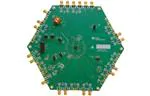
This user’s guide describes how to set up and operate the LMK01801 evaluation module (EVM). The
LMK01801 Evaluation Board simplifies evaluation of the LMK01801 Dual Clock Buffer Divider. Configuring
and controlling the board is accomplished using Texas Instrument’s TICS Pro software, which can be
downloaded from TI’s website: http://www.ti.com/tool/ticspro-sw. The LMK01801 can also be configured to
operate in a pin control mode via headers on the PCB.
Figure 1. LMK01801 EVAL
SNAU118A – December 2011 – Revised February 2018
Submit Documentation Feedback
Copyright © 2011–2018, Texas Instruments Incorporated
LMK01801 User’s Guide
1
�www.ti.com
Contents
Block Diagram ................................................................................................................ 3
Evaluation Board Kit Contents ............................................................................................. 4
Quick Start – SPI Mode (TICS Pro) ....................................................................................... 6
3.1
Quick Start – SPI Mode (TICS Pro) Description ................................................................ 7
4
Quick Start – Pin Control Mode ............................................................................................ 8
4.1
Quick Start – Pin Control Mode Description .................................................................... 9
4.2
Pin Control Modes .................................................................................................. 9
5
Using TICS Pro to Program the LMK01801 ............................................................................ 10
5.1
Start TICS Pro Application ....................................................................................... 10
5.2
Select Device ...................................................................................................... 10
5.3
Program/Load Device ............................................................................................. 10
5.4
Restoring a Default Mode ........................................................................................ 11
5.5
Enable Clock Outputs............................................................................................. 12
6
Evaluation Board Inputs/Outputs ......................................................................................... 14
7
Recommended Test Equipment .......................................................................................... 15
7.1
Power Supply ...................................................................................................... 15
7.2
Phase Noise / Spectrum Analyzer .............................................................................. 15
Appendix A
TICS Pro Usage ................................................................................................... 16
Appendix B
Typical Phase Noise Performance Plots ....................................................................... 21
Appendix C Schematics ......................................................................................................... 29
Appendix D Bill of Materials .................................................................................................... 37
Appendix E
Balun Information.................................................................................................. 40
Appendix F
Differential Voltage Measurement Terminology ............................................................... 41
1
2
3
List of Figures
LMK01801 EVAL
2
LMK01801 Block Diagram .................................................................................................. 4
3
Quick Start - SPI Mode Diagram
4
5
6
7
8
9
10
11
12
13
14
15
16
17
18
19
20
21
22
23
24
2
............................................................................................................
1
1
.......................................................................................... 6
Quick Start - Pin Control Mode Diagram ................................................................................. 8
Selecting the LMK01801 .................................................................................................. 10
Loading the Device ........................................................................................................ 11
Setting the Default Mode .................................................................................................. 11
Setting Divider, CLKout_TYPE, Enabled for CLKoutX on “Bank A” Page .......................................... 12
CLKout_TYPEs ............................................................................................................. 12
TICS Pro - User Controls Page .......................................................................................... 17
TICS Pro - Raw Registers Page ......................................................................................... 18
TICS Pro - Bank A Page .................................................................................................. 19
TICS Pro - Bank B Page .................................................................................................. 19
TICS Pro - Burst Page ..................................................................................................... 20
LMK01801 Phase Noise @ 100 MHz with Output Divider = 1 ....................................................... 22
LMK01801 Phase Noise @ 100 MHz with Output Divider = 4 ....................................................... 23
LMK01801 Phase Noise @ 983.04 MHz with Output Divider = 1 ................................................... 23
LMK01801 Phase Noise @ 983.04 MHz with Output Divider = 4 ................................................... 24
Phase Noise Measurement Set-Up ...................................................................................... 25
Noisy vs. Clean Phase Noise ............................................................................................. 26
LMK01801 Sample Clock Output Waveforms .......................................................................... 27
CLKout12 and CLKout13 No Analog Delay ............................................................................ 28
CLKout12 with 100 pSec of Delay Relative to CLKout13 ............................................................. 29
NOTE: The 51 Ω resistors R310 and R318 will need to be removed for the USB2ANY to assert
IC_SYNC0 and IC_SYNC1. .............................................................................................. 31
LMK01801 User’s Guide
SNAU118A – December 2011 – Revised February 2018
Submit Documentation Feedback
Copyright © 2011–2018, Texas Instruments Incorporated
�Block Diagram
www.ti.com
25
Typical Balun Frequency Response ..................................................................................... 40
26
Two Different Definitions for Differential Input Signals ................................................................ 41
27
Two Different Definitions for Differential Output Signals .............................................................. 42
List of Tables
1
Clock Output Configuration ................................................................................................. 4
2
EN_PIN_CTRL = LOW Configuration ..................................................................................... 9
3
EN_PIN_CTRL = HIGH Configuration .................................................................................... 9
4
LMK01801 Evaluation Board I/O ......................................................................................... 14
5
Phase Noise Output Test Configuration................................................................................. 21
6
LMK01801 Test Conditions ............................................................................................... 21
7
Clock Output Modes ....................................................................................................... 27
8
Common Bill of Materials for Evaluation Boards ....................................................................... 37
Trademarks
All trademarks are the property of their respective owners.
1
Block Diagram
Figure 2 illustrates the functional architecture of the LMK01801 clock divider buffer. The LMK01801 is a
very low noise solution for clocking systems that require distribution and frequency division of precision
clocks. The LMK01801 features extremely low residual noise, frequency division, digital and analog delay
adjustments, and fourteen (14) programmable differential outputs: LVPECL, LVDS and LVCMOS (2
outputs per differential output). The LMK01801 features two independent inputs that can be driven
differentially or in single-ended mode. The first input drives output Bank A consisting of eight (8) outputs.
The second input drives output Bank B consisting of six (6) outputs.
SNAU118A – December 2011 – Revised February 2018
Submit Documentation Feedback
Copyright © 2011–2018, Texas Instruments Incorporated
LMK01801 User’s Guide
3
�Evaluation Board Kit Contents
www.ti.com
CLKin1
CLKin1*
CLKin0
CLKin0*
Bank B
Bank A
Divider
(2-8)
CLKout0
CLKout0*
CLKout1
CLKout1*
CG4 Divider
CLKout2
CLKout2*
CLKout3
CLKout3*
LVDS/
LVPECL/
LVCMOS
CLKout4
CLKout4*
CLKout5
CLKout5*
LVDS/
LVPECL/
LVCMOS
CLKout6
CLKout6*
CLKout7
CLKout7*
Clock Distribution Path B
Clock Distribution Path A
CG1 Divider
Divider
(1-8)
LVDS/
LVPECL
Mux
Mux
LVDS/
LVPECL
CLKin1 Divider
CLKin0 Divider
Divider
(2-8)
Digital
Delay
Divider
(1-1045)
Analog
Delay
Mux
CLKout13
CLKout13*
LVDS/
LVPECL/
LVCMOS
Mux
CLKout12
CLKout12*
LVDS/
LVPECL/
LVCMOS
CLKout11
CLKout11*
CLKout10
CLKout10*
LVDS/
LVPECL/
LVCMOS
CLKout9
CLKout9*
CLKout8
CLKout8*
LVDS/
LVPECL/
LVCMOS
CG3 Divider
Divider
(1-8)
CG2 Divider
Divider
(1-8)
SYNC0/
CLKoutTYPE_1
SYNC1/
CLKoutTYPE_2
Test/
CLKoutTYPE_0
CLKuWire/
CLKoutDIV_1
Device
Control
DATAuWire/
CLKoutDIV_0
PWire
Port
Control
Registers
LEuWire/
CLKoutDIV_2
EN_PIN_CTRL
Figure 2. LMK01801 Block Diagram
2
Evaluation Board Kit Contents
The evaluation board kit contains:
• An LMK01801 Evaluation board.
• USB2ANY-UWIRE
– Evaluation board instructions are downloadable from the product folder on Texas Instruments’
website, http://www.ti.com/.
TICS Pro is the recommended program to program the evaluation board with the USB2ANY interface
adapter and the USB2ANY-uWire Adapter Board.
Table 1. Clock Output Configuration
4
Clock
Output Type
Output Connector Installed
0
LVPECL
Yes
1
LVPECL
No
2
LVPECL
Yes
3
LVPECL
No
4
LVPECL
Yes
5
LVPECL
No
6
LVPECL
Yes
7
LVPECL
No
8
LVPECL
Yes
LMK01801 User’s Guide
SNAU118A – December 2011 – Revised February 2018
Submit Documentation Feedback
Copyright © 2011–2018, Texas Instruments Incorporated
�Evaluation Board Kit Contents
www.ti.com
Table 1. Clock Output Configuration (continued)
Clock
Output Type
Output Connector Installed
9
LVPECL
Yes
10
LVPECL
Yes
11
LVPECL
Yes
12
LVPECL
Yes
13
LVPECL
Yes
SNAU118A – December 2011 – Revised February 2018
Submit Documentation Feedback
Copyright © 2011–2018, Texas Instruments Incorporated
LMK01801 User’s Guide
5
�Quick Start – SPI Mode (TICS Pro)
3.3 V
or
x
VC
USB cable
x
CL
CL Kout
Ko 0
u t0
*
Laptop or PC
VC
GN C
D
10-Pin Ribbon Cable
USB2ANY
Texas Instruments
3
5
HPA665
USB2ANY-uWire
Adapter Board
Program with TICS Pro
%H VXUH WR SUHVV ³&WUO+/´ RU 86%
communications Æ Write All Registers
4
C
DivVal0
Install jumpers except
on EN_PIN_CTRL
Type2
*
t1 0
o u t1 0
K
CL Kou
CL
DivVal1
DivVal2
Å BSL
Button
LMK01801
EN_PIN_CTRL
Type1
u t2
Ko 2*
CL Kout
CL
Type0
CL
CL Kout
Ko 8 *
ut8
CL
Kin
2
0*
Reference
Reference clock from
signal generator or
other external source.
CLKout6
CLKout6*
x
CLKin1*
CLKin1
Power
x
CLKout12*
CLKout12
1
x
CLKout13
CLKout13*
Quick Start – SPI Mode (TICS Pro)
CLKout4
CLKout4*
3
www.ti.com
Figure 3. Quick Start - SPI Mode Diagram
6
LMK01801 User’s Guide
SNAU118A – December 2011 – Revised February 2018
Submit Documentation Feedback
Copyright © 2011–2018, Texas Instruments Incorporated
�Quick Start – SPI Mode (TICS Pro)
www.ti.com
3.1
Quick Start – SPI Mode (TICS Pro) Description
1. Connect a voltage of 3.3 V to either the VCC SMA connector or the alternate terminal block.
2. Connect a reference clock from a signal generator or other source. Exact frequency depends on
programming.
3. Connect the PC to USB2ANY. Connect the USB2ANY-uWire Adapter Board from USB2ANY with a 10pin ribbon cable. Install jumpers as shown in Figure 3 and connect another 10-pin ribbon cable to the
uWire header on the EVM.
4. Install jumpers on TYPE0, TYPE1, TYPE2, DivVal0, DivVal1, DivVal2 in the middle uWire (pins 3,4)
position but NOT on EN_PIN_CTRL.
5. Program the device with TICS Pro. TICS Pro is available for download at http://www.ti.com/tool/ticsprosw.
1. Select USB2ANY mode from the Communication Setup window. To access this, select “USB
communications” → “Interface”. Confirm PC to USB communications by clicking “Identify” to see
blinking green LED on USB2ANY.
2. Select LMK04906 from the “Select Device” Menu. Click “Select Device” → “Clock Distribution with
Divider” → “LMK01801”.
3. Select a default mode from the “Default configuration” Menu. For the quick start, use “Default
configuration”.
4. Ctrl+L must be pressed at least once to load all registers. Alternatively click “USB
communications” → “Write All Registers” or the “Write All Registers” button on the Raw Registers
page.
6. Measurements may be made at any CLKout port via its SMA connector if enabled by programming.
NOTE: If required to assert SYNC signals through USB2ANY, remove resistors R310 and R318.
Refer to Section C.2 for details. This is not required for basic functionality. These resistors
terminate an external SYNC signal.
SNAU118A – December 2011 – Revised February 2018
Submit Documentation Feedback
Copyright © 2011–2018, Texas Instruments Incorporated
LMK01801 User’s Guide
7
�Quick Start – Pin Control Mode
Power
3.3 V
or
CLKin1*
CLKin1
1
CLKout12*
CLKout12
Quick Start – Pin Control Mode
CLKout13
CLKout13*
4
www.ti.com
VC
C
4
CL
CL Kout
Ko 0
ut0
*
VC
GN C
D
DivVal0
Install other jumpers ±
for output configuration
Type2
*
t1 0
ou t10
K
CL Kou
CL
DivVal1
DivVal2
LMK01801
EN_PIN_CTRL
Type1
ut2
Ko 2 *
CL Kout
CL
3
Install Jumper on
EN_PIN_CTRL
Type0
CL
CL Kout
Ko 8*
u t8
in 0
*
K
CL
CLKout6
CLKout6*
Reference
Reference clock from
signal generator or
other external source.
CLKout4
CLKout4*
2
Figure 4. Quick Start - Pin Control Mode Diagram
8
LMK01801 User’s Guide
SNAU118A – December 2011 – Revised February 2018
Submit Documentation Feedback
Copyright © 2011–2018, Texas Instruments Incorporated
�Quick Start – Pin Control Mode
www.ti.com
4.1
Quick Start – Pin Control Mode Description
1. Connect a voltage of 3.3 V to either the VCC SMA connector or the alternate connector.
2. Connect a reference clock from a signal generator or other source. Exact frequency depends on
programming.
3. Install a jumper on EN_PIN_CTRL header in either the High or Low position.
4. Install other jumpers on Type0, Type1, Type2, DivVal0, DivVal1, and DivVal2 headers based on the
configurations shown in Table 2 and Table 3.
4.2
Pin Control Modes
For Table 2 and Table 3, LOW is defined as installing a jumper between pins 5 and 6 on the desired
header. A HIGH is defined as installing a jumper between pins 1 and 2 on the desired header.
If EN_PIN_CTRL = LOW (jumper installed between header positions 5 and 6) then the following table
describes possible output configurations:
Table 2. EN_PIN_CTRL = LOW Configuration
Header
Type0
Output Groups
CLKout0 to CLKout3
CLKout4 to CLKout7
Header = Low
LVDS
Header = Middle
Powerdown
LVCMOS (Norm/Inv)
Header = High
LVPECL
Type1
CLKout8 to CLKout11
LVDS
LVCMOS (Norm/Inv)
LVPECL
Type2
CLKout12 to CLKout13
LVDS
LVCMOS (Norm/Inv)
LVPECL
DivVal0
CLKout0 to
CLKout3 Divider
÷1
÷4
÷2
DivVal1
CLKout4 to
CLKout7 Divider
÷1
÷4
÷2
CLKout8 to
CLKout11 Divider
÷1
÷4
÷2
CLKout12 to
CLKout13 Divider
÷8
÷512
÷16
DivVal2
If EN_PIN_CTRL = HIGH (jumper installed between header positions 1 and 2) then the following table
describes possible output configurations:
Table 3. EN_PIN_CTRL = HIGH Configuration
Header
Type0
Output Groups
CLKout0 to CLKout3
CLKout4 to CLKout7
Header = Low
LVDS
Header = Middle
LVPECL
LVCMOS (Norm/Inv)
Header = High
LVPECL
Type1
CLKout8 to CLKout11
LVDS
LVCMOS (Norm/Inv)
LVPECL
Type2
CLKout12 to CLKout13
LVDS
LVCMOS (Norm/Inv)
LVPECL
DivVal0
CLKout0 to
CLKout7 Dividers
÷1
÷4
÷2
DivVal1
CLKout8 to
CLKout11 Divider
÷1
÷4
÷2
DivVal2
CLKout12 to
CLKout13 Divider
÷4
÷512
÷16
SNAU118A – December 2011 – Revised February 2018
Submit Documentation Feedback
Copyright © 2011–2018, Texas Instruments Incorporated
LMK01801 User’s Guide
9
�Using TICS Pro to Program the LMK01801
5
www.ti.com
Using TICS Pro to Program the LMK01801
The purpose of this section is to walk the user through using TICS Pro to make some measurements with
the LMK01801 device. For more information on TICS Pro, refer to Appendix A. TICS Pro is available for
download at http://www.ti.com/tool/ticspro-sw.
Another option is to use CodeLoader4. The tool page for CodeLoader4 is located at
http://www.ti.com/tool/codeloader/.
Before proceeding, be sure to follow the Quick Start in Section 3 to ensure proper connections.
5.1
Start TICS Pro Application
Click “Start” → “Programs” → “Texas Instruments” → “TICS Pro”
The TICS Pro program is installed by default to the Texas Instruments application group.
5.2
Select Device
Click “Select Device” → “Clock Distribution with Divider” → “LMK01801”.
Once started, TICS Pro will load the last used device. To load a new device click “Select Device” from the
menu bar, then select the subgroup “Clock Distribution with Divider” and finally the device to load. For this
example, the LMK01801 is chosen. Selecting the device does cause the device to be programmed.
However, it is advisable to press “Ctrl+L” to ensure programming.
Figure 5. Selecting the LMK01801
5.3
Program/Load Device
Press “Ctrl+L”
Alternatively, click “USB communications” → “Write All Registers” from the menu to program the device to
the current state of the newly loaded LMK01801 file. “Ctrl+L” is the accelerator key assigned to the “Write
All Registers” option and is very convenient.
10
LMK01801 User’s Guide
SNAU118A – December 2011 – Revised February 2018
Submit Documentation Feedback
Copyright © 2011–2018, Texas Instruments Incorporated
�Using TICS Pro to Program the LMK01801
www.ti.com
Figure 6. Loading the Device
Once the device has been initially loaded, TICS Pro will automatically program changed registers, so it is
not necessary to reload the device upon subsequent changes in the device configuration. It is possible to
disable this functionality by ensuring there is no checkmark by the “Options” → “AutoUpdate”
Because a default mode will be restored in the next step, this step isn’t really needed but is included to
emphasize the importance of pressing “Ctrl+L” to load the device at least once after starting TICS Pro,
restoring a mode, or restoring a saved setup using the File menu.
5.4
Restoring a Default Mode
Click “Default configuration” → “Default Mode”; then
Press “Ctrl+L”
Figure 7. Setting the Default Mode
For the purposes of this walkthrough a default mode will be loaded to ensure a common starting point.
This is important because TICS Pro saves the state of the selected LMK01801 device when exiting the
software.
NOTE:
Loading a mode does not automatically program the device, so it is necessary to press
“Ctrl+L” again to program the device.
SNAU118A – December 2011 – Revised February 2018
Submit Documentation Feedback
Copyright © 2011–2018, Texas Instruments Incorporated
LMK01801 User’s Guide
11
�Using TICS Pro to Program the LMK01801
5.5
www.ti.com
Enable Clock Outputs
To
1.
2.
3.
measure phase noise at the clock outputs:
Click on the Bank A page.
Enable an output.
Then set the:
• CLKout Type
• Divide value
Figure 8. Setting Divider, CLKout_TYPE, Enabled for CLKoutX on “Bank A” Page
NOTE: This CLKoutX frequency value is only valid if the correct clock in value is specified. It may
not necessarily represent the actual frequency unless manually entered. This is a
mathematical calculation only, not a measured value.
4. Connect the clock output SMAs to a spectrum analyzer or signal source analyzer.
• For LVDS, a balun is recommended such as the ADT2-1T (for frequency range of 0.4 MHz to 450
MHz).
• For LVPECL
1. A balun can be used, or
2. One side of the LVPECL signal can be terminated with a 50-Ω load and the other side can be
run to the test equipment single ended.
• For LVCMOS
1. One side of the LVCMOS signal can be terminated with a 50-Ω load and the other side can be
run to the test equipment single ended.
Figure 9. CLKout_TYPEs
12
LMK01801 User’s Guide
SNAU118A – December 2011 – Revised February 2018
Submit Documentation Feedback
Copyright © 2011–2018, Texas Instruments Incorporated
�Using TICS Pro to Program the LMK01801
www.ti.com
5. The phase noise may be measured with a spectrum analyzer or signal source analyzer
See Appendix B for phase noise plots of the clock outputs
SNAU118A – December 2011 – Revised February 2018
Submit Documentation Feedback
Copyright © 2011–2018, Texas Instruments Incorporated
LMK01801 User’s Guide
13
�Evaluation Board Inputs/Outputs
6
www.ti.com
Evaluation Board Inputs/Outputs
Table 4 contains descriptions of the various inputs and outputs for the evaluation board.
Table 4. LMK01801 Evaluation Board I/O
Connector Name
Input/Output
Description
Output
Populated connectors.
Differential clock output pairs. All outputs are configured in
LVPECL mode.
On the evaluation board, all clock outputs are AC-coupled
to allow safe testing with RF test equipment.
All LVPECL/2VPECL clock outputs are terminated to GND
with a 240-Ω resistor, one on each output pin of the pair.
VCC
Input
Populated connector.
DC power supply for the PCB. Removing R1, R2, or R3
allow for splitting the power to various devices on the
board.
Note: The LMK01801 Family contains internal voltage
regulators for the VCO, PLL and related circuitry. The clock
outputs do not have an internal regulator. A clean power
supply is required for best performance.
VCC2
Input
Unpopulated connector.
Vcc input to power the output planes separately from the
Aux Plane. Refer to schematics for more information.
Input
Populated connectors.
The default board configuration is setup for a single-ended
reference source at CLKin0* (CLKin0 pin is AC-coupled to
ground).
If a DC-coupled clock is used to drive either of the inputs,
the high voltage level must be at least 2 volts and the low
voltage no greater than 0.4 volts.
CLKout0 / CLKout0*,
CLKout2 / CLKout2*,
CLKout4 / CLKout4*,
CLKout6 / CLKout6*,
CLKout8 / CLKout8,
CLKout9/ CLKout9*,
CLKout10 / CLKout10*,
CLKout11/ CLKout11*,
CLKout12 / CLKout12*,
CLKout13 / CLKout13*
CLKin0/CLKin0*,
CLKin1/CLKin1*
14
uWire
Input/Output
SYNC0,
SYNC1
Input
LMK01801 User’s Guide
Populated connector.
10-pin header programming interface for the board. Of
Most important are the CLKuWire, DATAuWire, and
LEuWire programming lines from this header. Each of
these signals, TEST, and SYNC0, and SYNC1 can be
monitored through test points on the board.
Unpopulated connector.
Access to SYNC0 or SYNC1 of device.
SNAU118A – December 2011 – Revised February 2018
Submit Documentation Feedback
Copyright © 2011–2018, Texas Instruments Incorporated
�Recommended Test Equipment
www.ti.com
7
Recommended Test Equipment
7.1
Power Supply
The Power Supply must be a low noise power supply.
7.2
Phase Noise / Spectrum Analyzer
For measuring phase noise an Agilent E5052A Signal Source Analyzer is recommended. An Agilent
E4445A PSA Spectrum Analyzer with the Phase Noise option is also usable although the architecture of
the E5052A is superior for phase noise measurements. At frequencies less than 100 MHz the local
oscillator noise of the E4445A is too high and measurements will reflect the E4445A’s internal local
oscillator performance, not the device under test.
SNAU118A – December 2011 – Revised February 2018
Submit Documentation Feedback
Copyright © 2011–2018, Texas Instruments Incorporated
LMK01801 User’s Guide
15
�Appendix A
SNAU118A – December 2011 – Revised February 2018
TICS Pro Usage
TICS Pro is the recommended program to program the evaluation board with the USB2ANY interface
adapter and the USB2ANY-uWire Adapter Board. TICS Pro can also be used to generate register maps
for programming the device. This appendix outlines the basic purpose and usage of each page. TICS Pro
is available for download at http://www.ti.com/tool/ticspro-sw.
A.1
TICS Pro Tips
•
A.2
Mousing over different controls will display some help prompt with the register address, data bit
location/length, and a brief register description in the lower left Context help pane.
Communication Setup
The USB communications window allows the USB2ANY or DemoMode to be selected. In case multiple
evaluation boards are to be connected and run with multiple instances of TICS Pro, the dropdown box will
allow specific USB2ANY devices to be selected. Pressing the identify button will identify which USB2ANY
is currently selected. Devices used by other instances of TICS Pro won’t display in this list.
16
TICS Pro Usage
SNAU118A – December 2011 – Revised February 2018
Submit Documentation Feedback
Copyright © 2011–2018, Texas Instruments Incorporated
�User Controls
www.ti.com
A.3
User Controls
The User Controls page has controls not included on one of the previously discussed dedicated pages.
Figure 10. TICS Pro - User Controls Page
SNAU118A – December 2011 – Revised February 2018
Submit Documentation Feedback
Copyright © 2011–2018, Texas Instruments Incorporated
TICS Pro Usage
17
�Raw Registers Page
A.4
www.ti.com
Raw Registers Page
The Raw Register page displays the register map including address. The address bits have the shaded
background and are not editable. The unshaded bits are the data bits. This register map may be directly
manipulated by clicking into the bit field, moving around with the arrow keys, and typing ‘1’ or ‘0’ to change
a bit.
All registers may be read or written in addition to individual registers. For individual register read/write, the
active register is highlighted in the list of registers and displayed in the top right. An individual register or
field may be read back by entering the name into the bottom right and clicking the “Read” button.
Register maps may be exported, but also imported. The import format may simply be the address and
register data in hex format as illustrated in the address/value column, one register to a line.
Figure 11. TICS Pro - Raw Registers Page
A.5
Bank A Page
The Bank A page allows control of the clock outputs format and other options relating to the clock
outputs, 0 through 7.
18
TICS Pro Usage
SNAU118A – December 2011 – Revised February 2018
Submit Documentation Feedback
Copyright © 2011–2018, Texas Instruments Incorporated
�Bank B Page
www.ti.com
Figure 12. TICS Pro - Bank A Page
A.6
Bank B Page
The Bank B page allows control of the clock outputs format and other options relating to the clock outputs
8 through 13. For outputs 12 and 13, the user can enable and set the clock output delay value.
Figure 13. TICS Pro - Bank B Page
SNAU118A – December 2011 – Revised February 2018
Submit Documentation Feedback
Copyright © 2011–2018, Texas Instruments Incorporated
TICS Pro Usage
19
�Burst Page
A.7
www.ti.com
Burst Page
The Burst page allows the user to program sequences of register programming or pin control.
Figure 14. TICS Pro - Burst Page
20
TICS Pro Usage
SNAU118A – December 2011 – Revised February 2018
Submit Documentation Feedback
Copyright © 2011–2018, Texas Instruments Incorporated
�Appendix B
SNAU118A – December 2011 – Revised February 2018
Typical Phase Noise Performance Plots
B.1
Clock Outputs
The LMK01801 Family features LVDS, LVPECL, 2VPECL, and LVCMOS types of outputs. Include are the
phase noise plots for the following outputs.
Table 5. Phase Noise Output Test Configuration
Device
CLKoutX
Output Divide
Output Type
8
1
LVPECL
8
4
LVPECL
8
1
2VPECL
8
4
2VPECL
4
1
LVDS
4
4
LVDS
4
1
LVCMOS(Norm/Inv)
4
4
LVCMOS(Norm/Inv)
LMK01801
B.2
Clock Output Measurement Technique
The measurement technique for each output type varies.
LVPECL/2VPECL – Measured by using an Minicircuits ADT2-1T balun on the input and on the output.
LVCMOS and LVDS – Measured by using an Minicircuits ADT2-1T balun on the output and single ended
input.
Table 6. LMK01801 Test Conditions
Parameter
Test Case 1
Test Case 2
Test Case 3
Test Case 4
Input Source
Wenzel XTAL
Wenzel XTAL
SMHU
Rohde & Schwarz
SMHU
Input Frequency
100 MHz
100 MHz
983.04 MHz
983.04 MHz
Input Power
0 dBm
0 dBm
0 dBm
0 dBm
Output Divider
1
4
1
4
Figure
Figure 15
Figure 16
Figure 17
Figure 18
SNAU118A – December 2011 – Revised February 2018
Submit Documentation Feedback
Typical Phase Noise Performance Plots
Copyright © 2011–2018, Texas Instruments Incorporated
21
�Clock Output Measurement Technique
B.2.1
www.ti.com
LMK01801 Phase Noise, CLKin = 100 MHz, Output Divider = 1
Figure 15. LMK01801 Phase Noise @ 100 MHz with Output Divider = 1
22
Typical Phase Noise Performance Plots
SNAU118A – December 2011 – Revised February 2018
Submit Documentation Feedback
Copyright © 2011–2018, Texas Instruments Incorporated
�Clock Output Measurement Technique
www.ti.com
B.2.2
LMK01801 Phase Noise, CLKin = 100 MHz, Output Divider = 4
Figure 16. LMK01801 Phase Noise @ 100 MHz with Output Divider = 4
B.2.3
LMK01801 Phase Noise, CLKin = 983.04 MHz, Output Divider = 1
Figure 17. LMK01801 Phase Noise @ 983.04 MHz with Output Divider = 1
SNAU118A – December 2011 – Revised February 2018
Submit Documentation Feedback
Typical Phase Noise Performance Plots
Copyright © 2011–2018, Texas Instruments Incorporated
23
�Clock Output Measurement Technique
B.2.4
www.ti.com
LMK01801 Phase Noise, CLKin = 983.04 MHz, Output Divider = 4
Figure 18. LMK01801 Phase Noise @ 983.04 MHz with Output Divider = 4
24
Typical Phase Noise Performance Plots
SNAU118A – December 2011 – Revised February 2018
Submit Documentation Feedback
Copyright © 2011–2018, Texas Instruments Incorporated
�Phase Noise Measurement
www.ti.com
B.3
Phase Noise Measurement
Power
Supply
Signal
Source
RF Output @
1 GHz, 0dBm
LMK01801
CLKin0 or
CLKin1
CLKoutX /
CLKoutX*
x
Agilent
5052A
x
x
x
x
Laptop or PC
Figure 19. Phase Noise Measurement Set-Up
The phase noise of the signal source will impact the measured phase noise of the LMK01801.
SNAU118A – December 2011 – Revised February 2018
Submit Documentation Feedback
Typical Phase Noise Performance Plots
Copyright © 2011–2018, Texas Instruments Incorporated
25
�Phase Noise Measurement
www.ti.com
Figure 20. Noisy vs. Clean Phase Noise
26
Typical Phase Noise Performance Plots
SNAU118A – December 2011 – Revised February 2018
Submit Documentation Feedback
Copyright © 2011–2018, Texas Instruments Incorporated
�LMK01801 Sample Output Waveforms
www.ti.com
B.4
LMK01801 Sample Output Waveforms
Figure 21. LMK01801 Sample Clock Output Waveforms
The output waveforms shown in Figure 21 were taken at a clock in frequency of 122.88 MHz, AC coupled.
These measurements follow the VID voltage convention – See Appendix F for more information.
The output modes are as follows:
Table 7. Clock Output Modes
B.5
Trace
Clock Output
Output Type
A
CLKout0
2VPECL
B
CLKout1
PECL (Low Power)
C
CLKout4
LVDS
D
CLKout5
LVCMOS (Normal/Invert)
LMK01801 Analog Delay Sample Data
The sample analog delay data was taken at a clock in frequency of 122.88 MHz, output format of
2VPECL. Notice in Figure 22 that with analog delay enabled there is approximately 460 ps of delay. Then,
in Figure 23, we added 100 ps of delay and the resulting delay is approximately 550 ps.
SNAU118A – December 2011 – Revised February 2018
Submit Documentation Feedback
Typical Phase Noise Performance Plots
Copyright © 2011–2018, Texas Instruments Incorporated
27
�LMK01801 Analog Delay Sample Data
www.ti.com
Figure 22. CLKout12 and CLKout13 No Analog Delay
28
Typical Phase Noise Performance Plots
SNAU118A – December 2011 – Revised February 2018
Submit Documentation Feedback
Copyright © 2011–2018, Texas Instruments Incorporated
�Figure 23. CLKout12 with 100 pSec of Delay Relative to CLKout13
Appendix C
SNAU118A – December 2011 – Revised February 2018
Schematics
SNAU118A – December 2011 – Revised February 2018
Submit Documentation Feedback
Copyright © 2011–2018, Texas Instruments Incorporated
Schematics
29
�Power Supply
C.1
30
www.ti.com
Power Supply
Schematics
SNAU118A – December 2011 – Revised February 2018
Submit Documentation Feedback
Copyright © 2011–2018, Texas Instruments Incorporated
�Main - LMK01801
www.ti.com
C.2
Main - LMK01801
Figure 24. NOTE: The 51 Ω resistors R310 and R318 will need to be removed for the USB2ANY to assert IC_SYNC0 and IC_SYNC1.
SNAU118A – December 2011 – Revised February 2018
Submit Documentation Feedback
Schematics
Copyright © 2011–2018, Texas Instruments Incorporated
31
�Inputs
C.3
Inputs
C.3.1
32
www.ti.com
Inputs Page 1
Schematics
SNAU118A – December 2011 – Revised February 2018
Submit Documentation Feedback
Copyright © 2011–2018, Texas Instruments Incorporated
�Inputs
www.ti.com
C.3.2
Inputs Page 2
SNAU118A – December 2011 – Revised February 2018
Submit Documentation Feedback
Schematics
Copyright © 2011–2018, Texas Instruments Incorporated
33
�Clock Outputs
C.4
Clock Outputs
C.4.1
34
www.ti.com
Clock Outputs Page 1
Schematics
SNAU118A – December 2011 – Revised February 2018
Submit Documentation Feedback
Copyright © 2011–2018, Texas Instruments Incorporated
�Clock Outputs
www.ti.com
C.4.2
Clock Outputs Page 2
SNAU118A – December 2011 – Revised February 2018
Submit Documentation Feedback
Schematics
Copyright © 2011–2018, Texas Instruments Incorporated
35
�Clock Outputs
C.4.3
36
www.ti.com
Clock Outputs Page 3
Schematics
SNAU118A – December 2011 – Revised February 2018
Submit Documentation Feedback
Copyright © 2011–2018, Texas Instruments Incorporated
�Appendix D
SNAU118A – December 2011 – Revised February 2018
Bill of Materials
D.1
Bill of Materials
Table 8. Common Bill of Materials for Evaluation Boards
Item Designator
Description
RoHS
Manufacturer
PartNumber
Quantity
1
C1, C7, C8, C10, C12,
C13, C16, C17, C18,
C19, C22, C23, C24,
C25, C28, C29, C30,
C31, C35, C36, C37,
C40, C41, C42, C43,
C46, C47, C48, C49,
C52, C53, C56, C301,
C302, C304, C314,
C321
CAP, CERM, 0.1 µF, 25 V, ±5%,
X7R, 0603
Y
Kemet
C0603C104J3RACT
U
37
2
C4
CAP, CERM, 100 pF, 50 V, ±5%,
C0G/NP0, 0603
Y
Kemet
C0603C101J5GACT
U
1
3
C5, C55, C313, C320,
C325, C328, C338,
C342, C359
CAP, CERM, 1 µF, 10 V, ±10%,
X5R, 0603
Y
Kemet
C0603C105K8PACT
U
9
4
C34, C326, C329, C339,
C343
CAP, CERM, 0.1 µF, 25 V, ±10%,
X7R, 0603
Y
Kemet
C0603C104K3RACT
U
5
5
C54, C303, C312, C319
CAP, CERM, 10 µF, 10 V, ±10%,
X5R, 0805
Y
Kemet
C0805C106K8PACT
U
4
6
C318, C348
CAP, CERM, 0.1 µF, 16 V, ±10%,
X7R, 0603
Y
TDK
C1608X7R1C104K
2
7
C341, C345
CAP, CERM, 1 µF, 16 V, ±10%,
X7R, 0603
Y
TDK
C1608X7R1C105K
2
8
C333, C346
CAP, CERM, 2200 pF, 100 V,
±5%, X7R, 0603
Y
AVX
06031C222JAT2A
2
9
C347
CAP, CERM, 10 µF, 10 V, ±20%,
X5R, 0805
Y
Kemet
C0805C106M8PAC
TU
1
10
C349
CAP, CERM, 4.7 µF, 10 V, ±10%,
X5R, 0603
Y
Kemet
C0603C475K8PACT
U
1
11
C337, C350
CAP, CERM, 0.01 µF, 25 V, ±5%,
C0G/NP0, 0603
Y
TDK
C1608C0G1E103J
2
12
C351, C352
CAP, CERM, 0.47 µF, 25 V, ±10%,
X7R, 0603
Y
MuRata
GRM188R71E474K
A12D
2
Connector, SMT, End launch SMA
50 Ohm
Y
Emerson
Network Power
142-0701-851
21
CAPACITORS
CONNECTORS
13
CLKin0*, CLKin1,
CLKin1*, CLKout0,
CLKout0*, CLKout2,
CLKout2*, CLKout4,
CLKout4*, CLKout6,
CLKout6*, CLKout8,
CLKout8*, CLKout10,
CLKout10*, CLKout12,
CLKout12*, CLKout13,
CLKout13*, Vcc, Vtune
SNAU118A – December 2011 – Revised February 2018
Submit Documentation Feedback
Copyright © 2011–2018, Texas Instruments Incorporated
Bill of Materials
37
�Bill of Materials
www.ti.com
Table 8. Common Bill of Materials for Evaluation Boards (continued)
Item Designator
14
J1
Description
RoHS
Manufacturer
PartNumber
Quantity
CONN TERM BLK PCB 5.08 MM
2POS OR
Y
Weidmuller
1594540000
1
RESISTORS
15
R2, R179, R303, R329,
R332, R334, R336,
R344, R346, R349
FB, 1000 Ω, 600 mA, 0603
Y
Murata
BLM18HE102SN1D
10
16
R3, R5, R10, R16, R17,
R21, R22, R301, R305,
R331, R335, R337,
R338, R347, R350,
R352, R356
RES, 0 Ω, 5%, 0.1 W, 0603
Y
Vishay-Dale
CRCW06030000Z0
EA
17
17
R4, R11
RES, 0 Ω, 5%, 0.125 W, 0805
Y
Vishay-Dale
CRCW08050000Z0
EA
2
18
R7, R30, R46, R52,
R68, R74, R90, R96,
R112, R118, R134,
R140, R156, R310,
R318
RES, 51.0 Ω, 1%, 0.1 W, 0603
Y
Yageo America
RC0603FR-0751RL
15
19
R20
RES, 100 Ω, 1%, 0.1 W, 0603
Y
Yageo America
RC0603FR07100RL
1
20
R31, R33, R39, R40,
R53, R55, R61, R62,
R75, R76, R83, R84,
R97, R98, R105, R106,
R119, R121, R127,
R128, R141, R143,
R149, R150, R163,
R165, R171, R172
RES, 240 Ω, 1%, 0.1 W, 0603
Y
Yageo America
RC0603FR07240RL
28
21
R35, R36, R57, R58,
R79, R80, R101, R102,
R123, R124, R145,
R146, R167, R168
RES, 68 Ω, 5%, 0.1 W, 0603
Y
Vishay-Dale
CRCW060368R0JN
EA
14
22
R302
RES, 39k Ω, 5%, 0.1 W, 0603
Y
Vishay-Dale
CRCW060339K0JN
EA
1
23
R311, R312, R315,
R320, R322, R325,
R328
RES, 27k Ω, 5%, 0.1 W, 0603
Y
Vishay-Dale
CRCW060327K0JN
EA
7
24
R308, R309, R314,
R317, R321, R324,
R327
RES, 15k Ω, 5%, 0.1 W, 0603
Y
Vishay-Dale
CRCW060315K0JN
EA
7
25
R342, R353, R357
RES, 51k Ω, 5%, 0.1 W, 0603
Y
Vishay-Dale
CRCW060351K0JN
EA
3
26
R343, R354
RES, 2.00k Ω, 1%, 0.1 W, 0603
Y
Vishay-Dale
CRCW06032K00FK
EA
2
27
R345, R355
RES, 866 Ω, 1%, 0.1 W, 0603
Y
Vishay-Dale
CRCW0603866RFK
EA
2
INTEGRATED CIRCUITS
28
38
U1
LMK01801
1
29
U300, U301
Micropower 800 mA Low Noise
'Ceramic Stable' Adjustable
Voltage Regulator for 1 V to 5 V
Applications
30
U302
Ultra Low Noise, 150 mA Linear
Regulator for RF/Analog Circuits
Requires No Bypass Capacitor
Y
Texas
Instruments
LP5900SD-3.3
1
31
uWire
Low Profile Vertical Header 2x5
0.100"
Y
FCI
52601-G10-8LF
1
Bill of Materials
Y
Texas
Instruments
LP3878SD-ADJ
2
SNAU118A – December 2011 – Revised February 2018
Submit Documentation Feedback
Copyright © 2011–2018, Texas Instruments Incorporated
�Bill of Materials
www.ti.com
Table 8. Common Bill of Materials for Evaluation Boards (continued)
Item Designator
32
DivVal0, DivVal1,
DivVal2,
EN_PIN_CONTROL,
TYPE0, TYPE1, TYPE2
Description
RoHS
Manufacturer
PartNumber
Quantity
Header, 2.54mm, 3x2, Gold, SMT
Y
Samtec
TSM-103-01-L-DV
7
USB2ANY-UWIRE
Y
Any
SV600857-001
1
Jumper, Shunt, 100mil, Gold
plated, Black
Y
3M
969102-0000-DA
7
0.875" Standoff
Y
VOLTREX
SPCS-14
6
OTHER
33
Kitting Item
34
SH_DivVal0_3-4,
SH_DivVal1_3-4,
SH_DivVal2_3-4,
SH_EN_PIN_CONTROL
_6-FLOAT,
SH_TYPE0_3-4,
SH_TYPE1_3-4,
SH_TYPE2_3-4
35
S1, S2, S3, S4, S5, S6
SNAU118A – December 2011 – Revised February 2018
Submit Documentation Feedback
Copyright © 2011–2018, Texas Instruments Incorporated
Bill of Materials
39
�Appendix E
SNAU118A – December 2011 – Revised February 2018
Balun Information
E.1
Typical Balun Frequency Response
The following figure illustrates the typical frequency response of the Mini-circuit’s ADT2-1T balun.
Figure 25. Typical Balun Frequency Response
40
Balun Information
SNAU118A – December 2011 – Revised February 2018
Submit Documentation Feedback
Copyright © 2011–2018, Texas Instruments Incorporated
�Appendix F
SNAU118A – December 2011 – Revised February 2018
Differential Voltage Measurement Terminology
F.1
The differential voltage of a differential signal can be described by two different definitions causing
confusion when reading datasheets or communicating with other engineers. This section will address the
measurement and description of a differential signal so that the reader will be able to understand and
discern between the two different definitions when used.
The first definition used to describe a differential signal is the absolute value of the voltage potential
between the inverting and non-inverting signal. The symbol for this first measurement is typically VID or
VOD depending on if an input or output voltage is being described.
The second definition used to describe a differential signal is to measure the potential of the noninverting
signal with respect to the inverting signal. The symbol for this second measurement is VSS and is a
calculated parameter. Nowhere in the IC does this signal exist with respect to ground, it only exists in
reference to its differential pair. VSS can be measured directly by oscilloscopes with floating references;
otherwise this value can be calculated as twice the value of VOD as described in the first section
Figure 26 illustrates the two different definitions side-by-side for inputs and Figure 27 illustrates the two
different definitions side-by-side for outputs. The VID and VOD definitions show VA and VB DC levels that
the non-inverting and inverting signals toggle between with respect to ground. VSS input and output
definitions show that if the inverting signal is considered the voltage potential reference, the non-inverting
signal voltage potential is now increasing and decreasing above and below the non-inverting reference.
Thus the peak-to-peak voltage of the differential signal can be measured.
VID and VOD are often defined in volts (V) and VSS is often defined as volts peak-to-peak (VPP).
VID Definition
VSS Definition for Input
Non-Inverting Clock
VA
VID
2*VID
VB
Inverting Clock
VID = | VA - VB |
VSS = 2*VID
GND
Figure 26. Two Different Definitions for Differential Input Signals
SNAU118A – December 2011 – Revised February 2018
Submit Documentation Feedback
Differential Voltage Measurement Terminology
Copyright © 2011–2018, Texas Instruments Incorporated
41
�www.ti.com
VOD Definition
VSS Definition for Output
Non-Inverting Clock
VA
VID
2*VOD
VB
Inverting Clock
VOD = | VA - VB |
VSS = 2*VOD
GND
Figure 27. Two Different Definitions for Differential Output Signals
42
Differential Voltage Measurement Terminology
SNAU118A – December 2011 – Revised February 2018
Submit Documentation Feedback
Copyright © 2011–2018, Texas Instruments Incorporated
�STANDARD TERMS FOR EVALUATION MODULES
1.
Delivery: TI delivers TI evaluation boards, kits, or modules, including any accompanying demonstration software, components, and/or
documentation which may be provided together or separately (collectively, an “EVM” or “EVMs”) to the User (“User”) in accordance
with the terms set forth herein. User's acceptance of the EVM is expressly subject to the following terms.
1.1 EVMs are intended solely for product or software developers for use in a research and development setting to facilitate feasibility
evaluation, experimentation, or scientific analysis of TI semiconductors products. EVMs have no direct function and are not
finished products. EVMs shall not be directly or indirectly assembled as a part or subassembly in any finished product. For
clarification, any software or software tools provided with the EVM (“Software”) shall not be subject to the terms and conditions
set forth herein but rather shall be subject to the applicable terms that accompany such Software
1.2 EVMs are not intended for consumer or household use. EVMs may not be sold, sublicensed, leased, rented, loaned, assigned,
or otherwise distributed for commercial purposes by Users, in whole or in part, or used in any finished product or production
system.
2
Limited Warranty and Related Remedies/Disclaimers:
2.1 These terms do not apply to Software. The warranty, if any, for Software is covered in the applicable Software License
Agreement.
2.2 TI warrants that the TI EVM will conform to TI's published specifications for ninety (90) days after the date TI delivers such EVM
to User. Notwithstanding the foregoing, TI shall not be liable for a nonconforming EVM if (a) the nonconformity was caused by
neglect, misuse or mistreatment by an entity other than TI, including improper installation or testing, or for any EVMs that have
been altered or modified in any way by an entity other than TI, (b) the nonconformity resulted from User's design, specifications
or instructions for such EVMs or improper system design, or (c) User has not paid on time. Testing and other quality control
techniques are used to the extent TI deems necessary. TI does not test all parameters of each EVM.
User's claims against TI under this Section 2 are void if User fails to notify TI of any apparent defects in the EVMs within ten (10)
business days after delivery, or of any hidden defects with ten (10) business days after the defect has been detected.
2.3 TI's sole liability shall be at its option to repair or replace EVMs that fail to conform to the warranty set forth above, or credit
User's account for such EVM. TI's liability under this warranty shall be limited to EVMs that are returned during the warranty
period to the address designated by TI and that are determined by TI not to conform to such warranty. If TI elects to repair or
replace such EVM, TI shall have a reasonable time to repair such EVM or provide replacements. Repaired EVMs shall be
warranted for the remainder of the original warranty period. Replaced EVMs shall be warranted for a new full ninety (90) day
warranty period.
3
Regulatory Notices:
3.1 United States
3.1.1
Notice applicable to EVMs not FCC-Approved:
FCC NOTICE: This kit is designed to allow product developers to evaluate electronic components, circuitry, or software
associated with the kit to determine whether to incorporate such items in a finished product and software developers to write
software applications for use with the end product. This kit is not a finished product and when assembled may not be resold or
otherwise marketed unless all required FCC equipment authorizations are first obtained. Operation is subject to the condition
that this product not cause harmful interference to licensed radio stations and that this product accept harmful interference.
Unless the assembled kit is designed to operate under part 15, part 18 or part 95 of this chapter, the operator of the kit must
operate under the authority of an FCC license holder or must secure an experimental authorization under part 5 of this chapter.
3.1.2
For EVMs annotated as FCC – FEDERAL COMMUNICATIONS COMMISSION Part 15 Compliant:
CAUTION
This device complies with part 15 of the FCC Rules. Operation is subject to the following two conditions: (1) This device may not
cause harmful interference, and (2) this device must accept any interference received, including interference that may cause
undesired operation.
Changes or modifications not expressly approved by the party responsible for compliance could void the user's authority to
operate the equipment.
FCC Interference Statement for Class A EVM devices
NOTE: This equipment has been tested and found to comply with the limits for a Class A digital device, pursuant to part 15 of
the FCC Rules. These limits are designed to provide reasonable protection against harmful interference when the equipment is
operated in a commercial environment. This equipment generates, uses, and can radiate radio frequency energy and, if not
installed and used in accordance with the instruction manual, may cause harmful interference to radio communications.
Operation of this equipment in a residential area is likely to cause harmful interference in which case the user will be required to
correct the interference at his own expense.
�FCC Interference Statement for Class B EVM devices
NOTE: This equipment has been tested and found to comply with the limits for a Class B digital device, pursuant to part 15 of
the FCC Rules. These limits are designed to provide reasonable protection against harmful interference in a residential
installation. This equipment generates, uses and can radiate radio frequency energy and, if not installed and used in accordance
with the instructions, may cause harmful interference to radio communications. However, there is no guarantee that interference
will not occur in a particular installation. If this equipment does cause harmful interference to radio or television reception, which
can be determined by turning the equipment off and on, the user is encouraged to try to correct the interference by one or more
of the following measures:
•
•
•
•
Reorient or relocate the receiving antenna.
Increase the separation between the equipment and receiver.
Connect the equipment into an outlet on a circuit different from that to which the receiver is connected.
Consult the dealer or an experienced radio/TV technician for help.
3.2 Canada
3.2.1
For EVMs issued with an Industry Canada Certificate of Conformance to RSS-210 or RSS-247
Concerning EVMs Including Radio Transmitters:
This device complies with Industry Canada license-exempt RSSs. Operation is subject to the following two conditions:
(1) this device may not cause interference, and (2) this device must accept any interference, including interference that may
cause undesired operation of the device.
Concernant les EVMs avec appareils radio:
Le présent appareil est conforme aux CNR d'Industrie Canada applicables aux appareils radio exempts de licence. L'exploitation
est autorisée aux deux conditions suivantes: (1) l'appareil ne doit pas produire de brouillage, et (2) l'utilisateur de l'appareil doit
accepter tout brouillage radioélectrique subi, même si le brouillage est susceptible d'en compromettre le fonctionnement.
Concerning EVMs Including Detachable Antennas:
Under Industry Canada regulations, this radio transmitter may only operate using an antenna of a type and maximum (or lesser)
gain approved for the transmitter by Industry Canada. To reduce potential radio interference to other users, the antenna type
and its gain should be so chosen that the equivalent isotropically radiated power (e.i.r.p.) is not more than that necessary for
successful communication. This radio transmitter has been approved by Industry Canada to operate with the antenna types
listed in the user guide with the maximum permissible gain and required antenna impedance for each antenna type indicated.
Antenna types not included in this list, having a gain greater than the maximum gain indicated for that type, are strictly prohibited
for use with this device.
Concernant les EVMs avec antennes détachables
Conformément à la réglementation d'Industrie Canada, le présent émetteur radio peut fonctionner avec une antenne d'un type et
d'un gain maximal (ou inférieur) approuvé pour l'émetteur par Industrie Canada. Dans le but de réduire les risques de brouillage
radioélectrique à l'intention des autres utilisateurs, il faut choisir le type d'antenne et son gain de sorte que la puissance isotrope
rayonnée équivalente (p.i.r.e.) ne dépasse pas l'intensité nécessaire à l'établissement d'une communication satisfaisante. Le
présent émetteur radio a été approuvé par Industrie Canada pour fonctionner avec les types d'antenne énumérés dans le
manuel d’usage et ayant un gain admissible maximal et l'impédance requise pour chaque type d'antenne. Les types d'antenne
non inclus dans cette liste, ou dont le gain est supérieur au gain maximal indiqué, sont strictement interdits pour l'exploitation de
l'émetteur
3.3 Japan
3.3.1
Notice for EVMs delivered in Japan: Please see http://www.tij.co.jp/lsds/ti_ja/general/eStore/notice_01.page 日本国内に
輸入される評価用キット、ボードについては、次のところをご覧ください。
http://www.tij.co.jp/lsds/ti_ja/general/eStore/notice_01.page
3.3.2
Notice for Users of EVMs Considered “Radio Frequency Products” in Japan: EVMs entering Japan may not be certified
by TI as conforming to Technical Regulations of Radio Law of Japan.
If User uses EVMs in Japan, not certified to Technical Regulations of Radio Law of Japan, User is required to follow the
instructions set forth by Radio Law of Japan, which includes, but is not limited to, the instructions below with respect to EVMs
(which for the avoidance of doubt are stated strictly for convenience and should be verified by User):
1.
2.
3.
Use EVMs in a shielded room or any other test facility as defined in the notification #173 issued by Ministry of Internal
Affairs and Communications on March 28, 2006, based on Sub-section 1.1 of Article 6 of the Ministry’s Rule for
Enforcement of Radio Law of Japan,
Use EVMs only after User obtains the license of Test Radio Station as provided in Radio Law of Japan with respect to
EVMs, or
Use of EVMs only after User obtains the Technical Regulations Conformity Certification as provided in Radio Law of Japan
with respect to EVMs. Also, do not transfer EVMs, unless User gives the same notice above to the transferee. Please note
that if User does not follow the instructions above, User will be subject to penalties of Radio Law of Japan.
�【無線電波を送信する製品の開発キットをお使いになる際の注意事項】 開発キットの中には技術基準適合証明を受けて
いないものがあります。 技術適合証明を受けていないもののご使用に際しては、電波法遵守のため、以下のいずれかの
措置を取っていただく必要がありますのでご注意ください。
1.
2.
3.
電波法施行規則第6条第1項第1号に基づく平成18年3月28日総務省告示第173号で定められた電波暗室等の試験設備でご使用
いただく。
実験局の免許を取得後ご使用いただく。
技術基準適合証明を取得後ご使用いただく。
なお、本製品は、上記の「ご使用にあたっての注意」を譲渡先、移転先に通知しない限り、譲渡、移転できないものとします。
上記を遵守頂けない場合は、電波法の罰則が適用される可能性があることをご留意ください。 日本テキサス・イ
ンスツルメンツ株式会社
東京都新宿区西新宿6丁目24番1号
西新宿三井ビル
3.3.3
Notice for EVMs for Power Line Communication: Please see http://www.tij.co.jp/lsds/ti_ja/general/eStore/notice_02.page
電力線搬送波通信についての開発キットをお使いになる際の注意事項については、次のところをご覧ください。http:/
/www.tij.co.jp/lsds/ti_ja/general/eStore/notice_02.page
3.4 European Union
3.4.1
For EVMs subject to EU Directive 2014/30/EU (Electromagnetic Compatibility Directive):
This is a class A product intended for use in environments other than domestic environments that are connected to a
low-voltage power-supply network that supplies buildings used for domestic purposes. In a domestic environment this
product may cause radio interference in which case the user may be required to take adequate measures.
4
EVM Use Restrictions and Warnings:
4.1 EVMS ARE NOT FOR USE IN FUNCTIONAL SAFETY AND/OR SAFETY CRITICAL EVALUATIONS, INCLUDING BUT NOT
LIMITED TO EVALUATIONS OF LIFE SUPPORT APPLICATIONS.
4.2 User must read and apply the user guide and other available documentation provided by TI regarding the EVM prior to handling
or using the EVM, including without limitation any warning or restriction notices. The notices contain important safety information
related to, for example, temperatures and voltages.
4.3 Safety-Related Warnings and Restrictions:
4.3.1
User shall operate the EVM within TI’s recommended specifications and environmental considerations stated in the user
guide, other available documentation provided by TI, and any other applicable requirements and employ reasonable and
customary safeguards. Exceeding the specified performance ratings and specifications (including but not limited to input
and output voltage, current, power, and environmental ranges) for the EVM may cause personal injury or death, or
property damage. If there are questions concerning performance ratings and specifications, User should contact a TI
field representative prior to connecting interface electronics including input power and intended loads. Any loads applied
outside of the specified output range may also result in unintended and/or inaccurate operation and/or possible
permanent damage to the EVM and/or interface electronics. Please consult the EVM user guide prior to connecting any
load to the EVM output. If there is uncertainty as to the load specification, please contact a TI field representative.
During normal operation, even with the inputs and outputs kept within the specified allowable ranges, some circuit
components may have elevated case temperatures. These components include but are not limited to linear regulators,
switching transistors, pass transistors, current sense resistors, and heat sinks, which can be identified using the
information in the associated documentation. When working with the EVM, please be aware that the EVM may become
very warm.
4.3.2
EVMs are intended solely for use by technically qualified, professional electronics experts who are familiar with the
dangers and application risks associated with handling electrical mechanical components, systems, and subsystems.
User assumes all responsibility and liability for proper and safe handling and use of the EVM by User or its employees,
affiliates, contractors or designees. User assumes all responsibility and liability to ensure that any interfaces (electronic
and/or mechanical) between the EVM and any human body are designed with suitable isolation and means to safely
limit accessible leakage currents to minimize the risk of electrical shock hazard. User assumes all responsibility and
liability for any improper or unsafe handling or use of the EVM by User or its employees, affiliates, contractors or
designees.
4.4 User assumes all responsibility and liability to determine whether the EVM is subject to any applicable international, federal,
state, or local laws and regulations related to User’s handling and use of the EVM and, if applicable, User assumes all
responsibility and liability for compliance in all respects with such laws and regulations. User assumes all responsibility and
liability for proper disposal and recycling of the EVM consistent with all applicable international, federal, state, and local
requirements.
5.
Accuracy of Information: To the extent TI provides information on the availability and function of EVMs, TI attempts to be as accurate
as possible. However, TI does not warrant the accuracy of EVM descriptions, EVM availability or other information on its websites as
accurate, complete, reliable, current, or error-free.
�6.
Disclaimers:
6.1 EXCEPT AS SET FORTH ABOVE, EVMS AND ANY MATERIALS PROVIDED WITH THE EVM (INCLUDING, BUT NOT
LIMITED TO, REFERENCE DESIGNS AND THE DESIGN OF THE EVM ITSELF) ARE PROVIDED "AS IS" AND "WITH ALL
FAULTS." TI DISCLAIMS ALL OTHER WARRANTIES, EXPRESS OR IMPLIED, REGARDING SUCH ITEMS, INCLUDING BUT
NOT LIMITED TO ANY EPIDEMIC FAILURE WARRANTY OR IMPLIED WARRANTIES OF MERCHANTABILITY OR FITNESS
FOR A PARTICULAR PURPOSE OR NON-INFRINGEMENT OF ANY THIRD PARTY PATENTS, COPYRIGHTS, TRADE
SECRETS OR OTHER INTELLECTUAL PROPERTY RIGHTS.
6.2 EXCEPT FOR THE LIMITED RIGHT TO USE THE EVM SET FORTH HEREIN, NOTHING IN THESE TERMS SHALL BE
CONSTRUED AS GRANTING OR CONFERRING ANY RIGHTS BY LICENSE, PATENT, OR ANY OTHER INDUSTRIAL OR
INTELLECTUAL PROPERTY RIGHT OF TI, ITS SUPPLIERS/LICENSORS OR ANY OTHER THIRD PARTY, TO USE THE
EVM IN ANY FINISHED END-USER OR READY-TO-USE FINAL PRODUCT, OR FOR ANY INVENTION, DISCOVERY OR
IMPROVEMENT, REGARDLESS OF WHEN MADE, CONCEIVED OR ACQUIRED.
7.
USER'S INDEMNITY OBLIGATIONS AND REPRESENTATIONS. USER WILL DEFEND, INDEMNIFY AND HOLD TI, ITS
LICENSORS AND THEIR REPRESENTATIVES HARMLESS FROM AND AGAINST ANY AND ALL CLAIMS, DAMAGES, LOSSES,
EXPENSES, COSTS AND LIABILITIES (COLLECTIVELY, "CLAIMS") ARISING OUT OF OR IN CONNECTION WITH ANY
HANDLING OR USE OF THE EVM THAT IS NOT IN ACCORDANCE WITH THESE TERMS. THIS OBLIGATION SHALL APPLY
WHETHER CLAIMS ARISE UNDER STATUTE, REGULATION, OR THE LAW OF TORT, CONTRACT OR ANY OTHER LEGAL
THEORY, AND EVEN IF THE EVM FAILS TO PERFORM AS DESCRIBED OR EXPECTED.
8.
Limitations on Damages and Liability:
8.1 General Limitations. IN NO EVENT SHALL TI BE LIABLE FOR ANY SPECIAL, COLLATERAL, INDIRECT, PUNITIVE,
INCIDENTAL, CONSEQUENTIAL, OR EXEMPLARY DAMAGES IN CONNECTION WITH OR ARISING OUT OF THESE
TERMS OR THE USE OF THE EVMS , REGARDLESS OF WHETHER TI HAS BEEN ADVISED OF THE POSSIBILITY OF
SUCH DAMAGES. EXCLUDED DAMAGES INCLUDE, BUT ARE NOT LIMITED TO, COST OF REMOVAL OR
REINSTALLATION, ANCILLARY COSTS TO THE PROCUREMENT OF SUBSTITUTE GOODS OR SERVICES, RETESTING,
OUTSIDE COMPUTER TIME, LABOR COSTS, LOSS OF GOODWILL, LOSS OF PROFITS, LOSS OF SAVINGS, LOSS OF
USE, LOSS OF DATA, OR BUSINESS INTERRUPTION. NO CLAIM, SUIT OR ACTION SHALL BE BROUGHT AGAINST TI
MORE THAN TWELVE (12) MONTHS AFTER THE EVENT THAT GAVE RISE TO THE CAUSE OF ACTION HAS
OCCURRED.
8.2 Specific Limitations. IN NO EVENT SHALL TI'S AGGREGATE LIABILITY FROM ANY USE OF AN EVM PROVIDED
HEREUNDER, INCLUDING FROM ANY WARRANTY, INDEMITY OR OTHER OBLIGATION ARISING OUT OF OR IN
CONNECTION WITH THESE TERMS, , EXCEED THE TOTAL AMOUNT PAID TO TI BY USER FOR THE PARTICULAR
EVM(S) AT ISSUE DURING THE PRIOR TWELVE (12) MONTHS WITH RESPECT TO WHICH LOSSES OR DAMAGES ARE
CLAIMED. THE EXISTENCE OF MORE THAN ONE CLAIM SHALL NOT ENLARGE OR EXTEND THIS LIMIT.
9.
Return Policy. Except as otherwise provided, TI does not offer any refunds, returns, or exchanges. Furthermore, no return of EVM(s)
will be accepted if the package has been opened and no return of the EVM(s) will be accepted if they are damaged or otherwise not in
a resalable condition. If User feels it has been incorrectly charged for the EVM(s) it ordered or that delivery violates the applicable
order, User should contact TI. All refunds will be made in full within thirty (30) working days from the return of the components(s),
excluding any postage or packaging costs.
10. Governing Law: These terms and conditions shall be governed by and interpreted in accordance with the laws of the State of Texas,
without reference to conflict-of-laws principles. User agrees that non-exclusive jurisdiction for any dispute arising out of or relating to
these terms and conditions lies within courts located in the State of Texas and consents to venue in Dallas County, Texas.
Notwithstanding the foregoing, any judgment may be enforced in any United States or foreign court, and TI may seek injunctive relief
in any United States or foreign court.
Mailing Address: Texas Instruments, Post Office Box 655303, Dallas, Texas 75265
Copyright © 2018, Texas Instruments Incorporated
�IMPORTANT NOTICE FOR TI DESIGN INFORMATION AND RESOURCES
Texas Instruments Incorporated (‘TI”) technical, application or other design advice, services or information, including, but not limited to,
reference designs and materials relating to evaluation modules, (collectively, “TI Resources”) are intended to assist designers who are
developing applications that incorporate TI products; by downloading, accessing or using any particular TI Resource in any way, you
(individually or, if you are acting on behalf of a company, your company) agree to use it solely for this purpose and subject to the terms of
this Notice.
TI’s provision of TI Resources does not expand or otherwise alter TI’s applicable published warranties or warranty disclaimers for TI
products, and no additional obligations or liabilities arise from TI providing such TI Resources. TI reserves the right to make corrections,
enhancements, improvements and other changes to its TI Resources.
You understand and agree that you remain responsible for using your independent analysis, evaluation and judgment in designing your
applications and that you have full and exclusive responsibility to assure the safety of your applications and compliance of your applications
(and of all TI products used in or for your applications) with all applicable regulations, laws and other applicable requirements. You
represent that, with respect to your applications, you have all the necessary expertise to create and implement safeguards that (1)
anticipate dangerous consequences of failures, (2) monitor failures and their consequences, and (3) lessen the likelihood of failures that
might cause harm and take appropriate actions. You agree that prior to using or distributing any applications that include TI products, you
will thoroughly test such applications and the functionality of such TI products as used in such applications. TI has not conducted any
testing other than that specifically described in the published documentation for a particular TI Resource.
You are authorized to use, copy and modify any individual TI Resource only in connection with the development of applications that include
the TI product(s) identified in such TI Resource. NO OTHER LICENSE, EXPRESS OR IMPLIED, BY ESTOPPEL OR OTHERWISE TO
ANY OTHER TI INTELLECTUAL PROPERTY RIGHT, AND NO LICENSE TO ANY TECHNOLOGY OR INTELLECTUAL PROPERTY
RIGHT OF TI OR ANY THIRD PARTY IS GRANTED HEREIN, including but not limited to any patent right, copyright, mask work right, or
other intellectual property right relating to any combination, machine, or process in which TI products or services are used. Information
regarding or referencing third-party products or services does not constitute a license to use such products or services, or a warranty or
endorsement thereof. Use of TI Resources may require a license from a third party under the patents or other intellectual property of the
third party, or a license from TI under the patents or other intellectual property of TI.
TI RESOURCES ARE PROVIDED “AS IS” AND WITH ALL FAULTS. TI DISCLAIMS ALL OTHER WARRANTIES OR
REPRESENTATIONS, EXPRESS OR IMPLIED, REGARDING TI RESOURCES OR USE THEREOF, INCLUDING BUT NOT LIMITED TO
ACCURACY OR COMPLETENESS, TITLE, ANY EPIDEMIC FAILURE WARRANTY AND ANY IMPLIED WARRANTIES OF
MERCHANTABILITY, FITNESS FOR A PARTICULAR PURPOSE, AND NON-INFRINGEMENT OF ANY THIRD PARTY INTELLECTUAL
PROPERTY RIGHTS.
TI SHALL NOT BE LIABLE FOR AND SHALL NOT DEFEND OR INDEMNIFY YOU AGAINST ANY CLAIM, INCLUDING BUT NOT
LIMITED TO ANY INFRINGEMENT CLAIM THAT RELATES TO OR IS BASED ON ANY COMBINATION OF PRODUCTS EVEN IF
DESCRIBED IN TI RESOURCES OR OTHERWISE. IN NO EVENT SHALL TI BE LIABLE FOR ANY ACTUAL, DIRECT, SPECIAL,
COLLATERAL, INDIRECT, PUNITIVE, INCIDENTAL, CONSEQUENTIAL OR EXEMPLARY DAMAGES IN CONNECTION WITH OR
ARISING OUT OF TI RESOURCES OR USE THEREOF, AND REGARDLESS OF WHETHER TI HAS BEEN ADVISED OF THE
POSSIBILITY OF SUCH DAMAGES.
You agree to fully indemnify TI and its representatives against any damages, costs, losses, and/or liabilities arising out of your noncompliance with the terms and provisions of this Notice.
This Notice applies to TI Resources. Additional terms apply to the use and purchase of certain types of materials, TI products and services.
These include; without limitation, TI’s standard terms for semiconductor products http://www.ti.com/sc/docs/stdterms.htm), evaluation
modules, and samples (http://www.ti.com/sc/docs/sampterms.htm).
Mailing Address: Texas Instruments, Post Office Box 655303, Dallas, Texas 75265
Copyright © 2018, Texas Instruments Incorporated
�