LMK03200
www.ti.com
SNAS478C – JULY 2009 – REVISED APRIL 2013
LMK03200 Family Precision 0-Delay Clock Conditioner with Integrated VCO
Check for Samples: LMK03200
1 Introduction
1.1
Features
12
• Integrated VCO with Very Low Phase Noise
Floor
• Integrated Integer-N PLL with Outstanding
Normalized Phase Noise Contribution of -224
dBc/Hz
• VCO Divider Values of 2 to 8 (All Divides)
– Bypassable with VCO Mux When Not in 0delay Mode
• Channel Divider Values of 1, 2 to 510 (Even
Divides)
• LVDS and LVPECL Clock Outputs
• Partially Integrated Loop Filter
1.2
•
•
•
•
•
•
• Dedicated Divider and Delay Blocks on Each
Clock Output
• 0-delay Outputs
• Internal or External Feedback of Output Clock
• Delay Blocks on N and R Phase Detector Inputs
for Lead/Lag Global Skew Adjust
• Pin Compatible Family of Clocking Devices
• 3.15 to 3.45 V Operation
• Package: 48 Pin WQFN (7.0 x 7.0 x 0.8 mm)
• 200 fs RMS Clock Generator Performance (10
Hz to 20 MHz) with a clean input clock
Target Applications
Data Converter Clocking
Networking, SONET/SDH, DSLAM
Wireless Infrastructure
Medical
Test and Measurement
Military / Aerospace
Recovered
³GLUW\´ FORFN RU
clean clock
VCO
Device
Outputs
LMK03200
3 LVDS
5 LVPECL
Tuning Range
(MHz)
RMS Jitter
(fs)
1185 - 1296
800
CLKout0
LMK03200
Family
OSCin
Precision Clock
Conditioner
Serializer/
Deserializer
CLKout1
CLKout4
CLKout7
LMX2531
PLL+VCO
FPGA
Fout
> 1 Gsps
ADC
1.3
DAC
0XOWLSOH ³FOHDQ´ FORFNV DW
different frequencies
Description
The LMK03200 family of precision clock conditioners combine the functions of jitter
cleaning/reconditioning, multiplication, and 0-delay distribution of a reference clock. The devices integrate
a Voltage Controlled Oscillator (VCO), a high performance Integer-N Phase Locked Loop (PLL), a partially
integrated loop filter, and up to eight outputs in various LVDS and LVPECL combinations.
The VCO output is optionally accessible on the Fout port. Internally, the VCO output goes through a VCO
divider to feed the various clock distribution blocks.
1
2
Please be aware that an important notice concerning availability, standard warranty, and use in critical applications of
Texas Instruments semiconductor products and disclaimers thereto appears at the end of this data sheet.
All trademarks are the property of their respective owners.
PRODUCTION DATA information is current as of publication date. Products conform to
specifications per the terms of the Texas Instruments standard warranty. Production
processing does not necessarily include testing of all parameters.
Copyright © 2009–2013, Texas Instruments Incorporated
�LMK03200
SNAS478C – JULY 2009 – REVISED APRIL 2013
www.ti.com
Each clock distribution block includes a programmable divider, a phase synchronization circuit, a
programmable delay, a clock output mux, and an LVDS or LVPECL output buffer. The PLL also features
delay blocks to permit global phase adjustment of clock output phase. This allows multiple integer-related
and phase-adjusted copies of the reference to be distributed to eight system components.
The clock conditioners come in a 48-pin WQFN package and are footprint compatible with other clocking
devices in the same family.
1
.............................................. 1
............................................. 1
1.2
Target Applications .................................. 1
1.3
Description ........................................... 1
Device Information ...................................... 3
2.1
Functional Block Diagram ........................... 3
2.2
Connection Diagram ................................. 3
Electrical Specifications ............................... 5
3.1
Absolute Maximum Ratings .......................... 5
3.2
Recommended Operating Conditions ............... 5
3.3
Package Thermal Resistance ....................... 5
3.4
Electrical Characteristics ............................ 6
3.5
Serial Data Timing Diagram ........................ 10
3.6
Charge Pump Current Specification Definitions .... 11
Typical Performance Characteristics ............. 12
Functional Description ............................... 14
5.1
BIAS PIN ........................................... 14
5.2
LDO BYPASS ...................................... 14
5.3
OSCILLATOR INPUT PORT (OSCin, OSCin*) .... 14
5.4
LOW NOISE, FULLY INTEGRATED VCO ......... 14
5.5
LVDS/LVPECL OUTPUTS ......................... 15
Introduction
1.1
2
3
4
5
Features
5.6
GLOBAL CLOCK OUTPUT SYNCHRONIZATION
5.7
CLKout OUTPUT STATES
5.8
GLOBAL OUTPUT ENABLE AND LOCK DETECT
16
5.9
...............................
DIGITAL LOCK DETECT ...........................
CLKout DELAYS ...................................
GLOBAL DELAYS ..................................
VCO DIVIDER BYPASS MODE ....................
16
POWER ON RESET
5.10
5.11
5.12
5.13
2
.........................
15
16
17
17
17
18
5.14
6
6.1
6.2
6.3
7
0-DELAY MODE
....................................
................
General Programming Information
18
19
Recommended Programming Sequence, without 0Delay Mode ......................................... 19
Recommended Programing Sequence, with 0-Delay
Mode ................................................ 19
Recommended Programming Sequence, bypassing
VCO divider ......................................... 23
..................................
.........................................
6.6
Register R9 .........................................
6.7
Register R11 ........................................
6.8
Register R13 ........................................
6.9
Register R14 ........................................
6.10 REGISTER R15 ....................................
Application Information ..............................
7.1
SYSTEM LEVEL DIAGRAM ........................
7.2
BIAS PIN ...........................................
7.3
LDO BYPASS ......................................
7.4
LOOP FILTER ......................................
6.4
Register R0 to R7
28
6.5
Register R8
32
32
32
33
34
37
39
39
39
39
7.5
40
CURRENT CONSUMPTION / POWER
DISSIPATION CALCULATIONS ................... 41
7.6
7.7
THERMAL MANAGEMENT ........................ 42
TERMINATION AND USE OF CLOCK OUTPUTS
(DRIVERS) ......................................... 43
7.8
7.9
OSCin INPUT ...................................... 46
MORE THAN EIGHT OUTPUTS WITH AN
LMK03200 FAMILY DEVICE ....................... 47
DIFFERENTIAL VOLTAGE MEASUREMENT
TERMINOLOGY .................................... 47
7.10
Revision History
Contents
............................................
48
Copyright © 2009–2013, Texas Instruments Incorporated
Submit Documentation Feedback
Product Folder Links: LMK03200
�LMK03200
www.ti.com
SNAS478C – JULY 2009 – REVISED APRIL 2013
2 Device Information
Functional Block Diagram
Partially
Integrated
Loop Filter
CPout
2.1
OSCin
OSCin*
R Divider
R Delay
N Divider
N Delay
Internal
VCO
Phase
Detector
Fout
Distribution Path
VCO
Mux
Ndiv
Mux
VCO
Divider
FBCLKin
FBCLKin*
FB
Mux
CLKout0
CLKout0*
Mux
CLKout1
CLKout1*
Mux
CLKout2
CLKout2*
Mux
CLKout3
CLKout3*
Mux
Divider
Divider
Delay
Mux
CLKout4
CLKout4*
Mux
CLKout5
CLKout5*
Mux
CLKout6
CLKout6*
Mux
CLKout7
CLKout7*
Delay
Divider
Divider
Delay
Delay
Divider
Divider
Delay
Delay
Divider
Divider
Delay
Delay
Low Clock Buffers
High Clock Buffers
CLK
DATA
PWire
Port
GOE
Control
Registers
SYNC*
LE
LD
CLKout7*
CLKout7
Vcc14
CLKout6*
CLKout6
Vcc13
CLKout5*
CLKout5
Vcc12
CLKout4*
CLKout4
Vcc11
Connection Diagram
48
47
46
45
44
43
42
41
40
39
38
37
GND
1
36
Bias
Fout
2
35
FBCLKin*
Vcc1
3
34
FBCLKin
CLKuWire
4
33
Vcc10
DATAuWire
5
32
CPout
LEuWire
6
31
Vcc9
NC
7
30
Vcc8
Vcc2
8
29
OSCin*
LDObyp1
9
28
OSCin
LDObyp2
10
27
SYNC*
GOE
11
26
Vcc7
LD
12
25
GND
Top Down View
14
15
16
17
18
19
20
21
22
23
24
Vcc4
CLKout1
CLKout1*
Vcc5
CLKout2
CLKout2*
Vcc6
CLKout3
CLKout3*
Vcc3
13
CLKout0*
DAP
CLKout0
2.2
Device
Control
Figure 2-1. 48-Pin WQFN Package
Device Information
Copyright © 2009–2013, Texas Instruments Incorporated
Submit Documentation Feedback
Product Folder Links: LMK03200
3
�LMK03200
SNAS478C – JULY 2009 – REVISED APRIL 2013
www.ti.com
Table 2-1. PIN DESCRIPTIONS
4
Pin #
Pin Name
I/O
1, 25
GND
-
Ground
Description
2
Fout
O
Internal VCO Frequency Output
3, 8, 13, 16, 19, 22,
26, 30, 31, 33, 37,
40, 43, 46
Vcc1, Vcc2, Vcc3, Vcc4, Vcc5, Vcc6, Vcc7, Vcc8, Vcc9, Vcc10,
Vcc11, Vcc12, Vcc13, Vcc14
-
Power Supply
4
CLKuWire
I
MICROWIRE Clock Input
5
DATAuWire
I
MICROWIRE Data Input
6
LEuWire
I
MICROWIRE Latch Enable Input
7
NC
-
No Connection to these pins
9, 10
LDObyp1, LDObyp2
-
LDO Bypass
11
GOE
I
Global Output Enable
12
LD
O
Lock Detect and Test Output
14, 15
CLKout0, CLKout0*
O
LVDS Clock Output 0
17, 18
CLKout1, CLKout1*
O
LVDS Clock Output 1
20, 21
CLKout2, CLKout2*
O
LVDS Clock Output 2
23, 24
CLKout3, CLKout3*
O
LVPECL Clock Output 3
27
SYNC*
I
Global Clock Output Synchronization
28, 29
OSCin, OSCin*
I
Oscillator Clock Input; Should be AC
coupled
32
CPout
O
Charge Pump Output
34, 35
FBCLKin, FBCLKin*
I
External Feedback Clock Input for 0-delay
mode
36
Bias
I
Bias Bypass
38, 39
CLKout4, CLKout4*
O
LVPECL Clock Output 4
41, 42
CLKout5, CLKout5*
O
LVPECL Clock Output 5
44, 45
CLKout6, CLKout6*
O
LVPECL Clock Output 6
47, 48
CLKout7, CLKout7*
O
LVPECL Clock Output 7
DAP
DAP
-
Die Attach Pad is Ground
Device Information
Copyright © 2009–2013, Texas Instruments Incorporated
Submit Documentation Feedback
Product Folder Links: LMK03200
�LMK03200
www.ti.com
SNAS478C – JULY 2009 – REVISED APRIL 2013
These devices have limited built-in ESD protection. The leads should be shorted together or the device placed in conductive foam
during storage or handling to prevent electrostatic damage to the MOS gates.
3 Electrical Specifications
3.1
Absolute Maximum Ratings (1) (2) (3)
Symbol
Ratings
Units
Power Supply Voltage
Parameter
VCC
-0.3 to 3.6
V
Input Voltage
VIN
-0.3 to (VCC + 0.3)
V
Storage Temperature Range
TSTG
-65 to 150
°C
Lead Temperature (solder 4 s)
TL
+260
°C
Junction Temperature
TJ
125
°C
(1)
(2)
(3)
3.2
"Absolute Maximum Ratings" indicate limits beyond which damage to the device may occur, including inoperability and degradation of
device reliability and/or performance. Functional operation of the device and/or non-degradation at the Absolute Maximum Ratings or
other conditions beyond those indicated in the Recommended Operating Conditions is not implied. The Recommended Operating
Conditions indicate conditions at which the device is functional and the device should not be operated beyond such conditions.
This device is a high performance integrated circuit with ESD handling precautions. Handling of this device should only be done at ESD
protected work stations. The device is rated to a HBM-ESD of > 2 kV, a MM-ESD of > 200 V, and a CDM-ESD of > 1.2 kV.
If Military/Aerospace specified devices are required, please contact the Texas Instruments Sales Office/Distributors for availability and
specifications.
Recommended Operating Conditions
Symbol
Min
Typ
Max
Units
Ambient Temperature
Parameter
TA
-40
25
85
°C
Power Supply Voltage
VCC
3.15
3.3
3.45
V
3.3
Package Thermal Resistance
Package
48-Lead WQFN
(1)
(1)
θJA
θJ-PAD (Thermal Pad)
27.4° C/W
5.8° C/W
Specification assumes 16 thermal vias connect the die attach pad to the embedded copper plane on the 4-layer JEDEC board. These
vias play a key role in improving the thermal performance of the WQFN. It is recommended that the maximum number of vias be used in
the board layout.
Electrical Specifications
Copyright © 2009–2013, Texas Instruments Incorporated
Submit Documentation Feedback
Product Folder Links: LMK03200
5
�LMK03200
SNAS478C – JULY 2009 – REVISED APRIL 2013
3.4
Electrical Characteristics
www.ti.com
(1)
(3.15 V ≤ Vcc ≤ 3.45 V, -40 °C ≤ TA ≤ 85 °C, Differential Inputs/Outputs; Vboost=0; except as specified. Typical values
represent most likely parametric norms at Vcc = 3.3 V, TA = 25 °C, and at the Recommended Operation Conditions at the
time of product characterization and are not guaranteed).
Symbol
Parameter
Conditions
Min
Typ
Max
Units
Current Consumption
Entire device; one LVDS and one
LVPECL clock enabled; no divide; no
delay.
Power Supply Current
ICC
(2)
ICCPD
Power Down Current
161.8
mA
Entire device; All Outputs Off (no
emitter resistors placed)
86
POWERDOWN = 1
5
mA
Reference Oscillator Input
fOSCin
Reference Oscillator Input Frequency
Range
VIDOSCin
Reference Oscillator Differential Input
Voltage (3) (4)
VOSCin
Reference Oscillator Single-ended Input
Voltage (4)
SLEWOSCin
Reference Oscillator Input Slew Rate
(4)
1
200
MHz
AC coupled
0.2
1.6
V
AC coupled; Unused pin AC coupled to
GND
0.2
2.0
Vpp
20% to 80%; For each input pin
0.15
0.5
V/ns
External Feedback Clock Input
fFBCLKin
External Feedback Clock Input Frequency
Range
VIDFBCLKin
External Feedback Clock Differential Input
Voltage (3) (4)
VFBCLKin
External Feedback Clock Single-ended
Input Voltage (4)
SLEWFBCLKin
(1)
(2)
(3)
(4)
6
External Feedback Clock Input Slew Rate
(4)
1
800
MHz
AC coupled
0.2
1.6
V
AC coupled; Unused pin AC coupled to
GND
0.2
2.0
Vpp
20% to 80%; For each input pin
0.15
0.5
V/ns
The Electrical Characteristics table lists ensured specifications under the listed Recommended Operating Conditions except as
otherwise modified or specified by the Electrical Characteristics Conditions and/or Notes. Typical specifications are estimations only and
are not ensured.
See Section Section 7.5 for more information.
See Section Section 7.10 for more information.
Specification is ensured by characterization and is not tested in production.
Electrical Specifications
Copyright © 2009–2013, Texas Instruments Incorporated
Submit Documentation Feedback
Product Folder Links: LMK03200
�LMK03200
www.ti.com
SNAS478C – JULY 2009 – REVISED APRIL 2013
Electrical Characteristics (1) (continued)
(3.15 V ≤ Vcc ≤ 3.45 V, -40 °C ≤ TA ≤ 85 °C, Differential Inputs/Outputs; Vboost=0; except as specified. Typical values
represent most likely parametric norms at Vcc = 3.3 V, TA = 25 °C, and at the Recommended Operation Conditions at the
time of product characterization and are not guaranteed).
Symbol
Parameter
Conditions
Min
Typ
Max
Units
40
MHz
PLL
fPD
Phase Detector Frequency
VCPout = Vcc/2, PLL_CP_GAIN = 1x
ISRCECPout
Charge Pump Source Current
100
VCPout = Vcc/2, PLL_CP_GAIN = 4x
400
VCPout = Vcc/2, PLL_CP_GAIN = 16x
1600
VCPout = Vcc/2, PLL_CP_GAIN = 32x
3200
VCPout = Vcc/2, PLL_CP_GAIN = 1x
-100
VCPout = Vcc/2, PLL_CP_GAIN = 4x
-400
VCPout = Vcc/2, PLL_CP_GAIN = 16x
-1600
VCPout = Vcc/2, PLL_CP_GAIN = 32x
-3200
µA
μA
ISINKCPout
Charge Pump Sink Current
ICPoutTRI
Charge Pump TRI-STATE Current
0.5 V < VCPout < Vcc - 0.5 V
2
ICPout%MIS
Magnitude of Charge Pump
Sink vs. Source Current Mismatch
VCPout = Vcc / 2
TA = 25°C
3
%
ICPoutVTUNE
Magnitude of Charge Pump
Current vs. Charge Pump Voltage Variation
0.5 V < VCPout < Vcc - 0.5 V
TA = 25°C
4
%
ICPoutTEMP
Magnitude of Charge Pump Current vs.
Temperature Variation
4
%
PN10kHz
PLL 1/f Noise at 10 kHz Offset (1)
Normalized to 1 GHz Output Frequency
PLL_CP_GAIN = 1x
-117
PLL_CP_GAIN = 32x
-122
Normalized Phase Noise Contribution
PLL_CP_GAIN = 1x
-219
PLL_CP_GAIN = 32x
-224
PN1Hz
(1)
(2)
(2)
10
nA
dBc/Hz
dBc/Hz
A specification in modeling PLL in-band phase noise is the 1/f flicker noise, LPLL_flicker(f), which is dominant close to the carrier. Flicker
noise has a 10 dB/decade slope. PN10kHz is normalized to a 10 kHz offset and a 1 GHz carrier frequency. PN10kHz = LPLL_flicker(10
kHz) - 20log(Fout / 1 GHz), where LPLL_flicker(f) is the single side band phase noise of only the flicker noise's contribution to total noise,
L(f). To measure LPLL_flicker(f) it is important to be on the 10 dB/decade slope close to the carrier. A high compare frequency and a clean
crystal are important to isolating this noise source from the total phase noise, L(f). LPLL_flicker(f) can be masked by the reference
oscillator performance if a low power or noisy source is used. The total PLL in-band phase noise performance is the sum of LPLL_flicker(f)
and LPLL_flat(f).
A specification in modeling PLL in-band phase noise is the Normalized Phase Noise Contribution, LPLL_flat(f), of the PLL and is defined
as PN1Hz = LPLL_flat(f) – 20log(N) – 10log(fCOMP). LPLL_flat(f) is the single side band phase noise measured at an offset frequency, f, in a
1 Hz Bandwidth and fCOMP is the phase detector frequency of the synthesizer. LPLL_flat(f) contributes to the total noise, L(f). To measure
LPLL_flat(f) the offset frequency, f, must be chosen sufficiently smaller then the loop bandwidth of the PLL, and yet large enough to avoid
a substantial noise contribution from the reference and flicker noise. LPLL_flat(f) can be masked by the reference oscillator performance if
a low power or noisy source is used.
Electrical Specifications
Copyright © 2009–2013, Texas Instruments Incorporated
Submit Documentation Feedback
Product Folder Links: LMK03200
7
�LMK03200
SNAS478C – JULY 2009 – REVISED APRIL 2013
www.ti.com
Electrical Characteristics (1) (continued)
(3.15 V ≤ Vcc ≤ 3.45 V, -40 °C ≤ TA ≤ 85 °C, Differential Inputs/Outputs; Vboost=0; except as specified. Typical values
represent most likely parametric norms at Vcc = 3.3 V, TA = 25 °C, and at the Recommended Operation Conditions at the
time of product characterization and are not guaranteed).
Symbol
Parameter
Conditions
Min
Typ
Max
Units
1296
MHz
125
°C
VCO
fFout
|ΔTCL|
VCO Tuning Range
LMK03200
Allowable Temperature Drift for Continuous
Lock
After programming R15 for lock, only
changes 0_DELAY_MODE and PLL_N
for the purpose of enabling 0-delay
mode permitted to ensure continuous
lock. (1)
Output Power to a 50 Ω load driven by Fout
pFout
(2)
(3)
KVCO
Fine Tuning Sensitivity
JRMSFout
Fout RMS Period Jitter
(12 kHz to 20 MHz bandwidth)
1185
LMK03200; TA = 25 °C
3.3
dBm
LMK03200
7 to 9
MHz/V
LMK03200
800
fs
Clock Skew and Delay
tSKEWLVDS
CLKoutX to CLKoutY
(4)
tSKEWLVPEC
L
CLKoutX to CLKoutY
(4)
td0-DELAY
(1)
(2)
(3)
(4)
8
OSCin to CLKoutX delay
(4)
Equal loading and identical clock
configuration
RL = 100 Ω
-30
±4
30
ps
Equal loading and identical clock
configuration
RL = 100 Ω
-30
±3
30
ps
0-Delay mode active; PLL_N_DLY = 0;
PLL_R_DLY = 0; FB_MUX = 0
(CLKout5)
-300
-65
300
0-Delay mode active; PLL_N_DLY = 0;
PLL_R_DLY = 0; FB_MUX = 2
(CLKout6)
-300
35
300
0-Delay mode active; PLL_N_DLY = 0;
PLL_R_DLY = 0; FB_MUX = 1
(FBCLKin)
-700
-400
-100
0-Delay mode active; PLL_N_DLY = 0;
PLL_R_DLY = 3; FB_MUX = 1
(FBCLKin)
-400
35
400
ps
Allowable Temperature Drift for Continuous Lock is how far the temperature can drift in either direction and stay in lock from the ambient
temperature and programmed state at which the device was when the frequency calibration routine was run. The action of programming
the R15 register, even to the same value, when 0_DELAY_MODE = 0 activates a frequency calibration routine. This implies that the
device will work over the entire frequency range, but if the temperature drifts more than the maximum allowable drift for continuous lock,
then it will be necessary to reprogram the R15 register while 0_DELAY_MODE = 0 to ensure that the device stays in lock. Regardless of
what temperature the device was initially programmed at, the ambient temperature can never drift outside the range of -40 °C ≤ TA ≤ 85
°C without violating specifications. For this specification to be valid, the programmed state of the device must not change after R15 is
programmed except for 0_DELAY_MODE and PLL_N for the purpose of enabling 0-delay mode.
Output power varies as a function of frequency. When a range is shown, the higher output power applies to the lower frequency and the
lower output power applies to the higher frequency.
The lower sensitivity indicates the typical sensitivity at the lower end of the tuning range, the higher sensitivity at the higher end of the
tuning range
Specification is ensured by characterization and is not tested in production.
Electrical Specifications
Copyright © 2009–2013, Texas Instruments Incorporated
Submit Documentation Feedback
Product Folder Links: LMK03200
�LMK03200
www.ti.com
SNAS478C – JULY 2009 – REVISED APRIL 2013
Electrical Characteristics (1) (continued)
(3.15 V ≤ Vcc ≤ 3.45 V, -40 °C ≤ TA ≤ 85 °C, Differential Inputs/Outputs; Vboost=0; except as specified. Typical values
represent most likely parametric norms at Vcc = 3.3 V, TA = 25 °C, and at the Recommended Operation Conditions at the
time of product characterization and are not guaranteed).
Symbol
Parameter
Conditions
Min
Typ
Max
Units
Clock Distribution Section - LVDS Clock Outputs (1)
JitterADD
Additive RMS Jitter
RL = 100 Ω
Distribution Path =
765 MHz
Bandwidth =
12 kHz to 20 MHz
(1)
CLKoutX_MUX =
Bypass (no
divide or delay)
20
CLKoutX_MUX =
Divided (no
delay)
CLKoutX_DIV =
4
75
fs
VOD
Differential Output Voltage
RL = 100 Ω
250
ΔVOD
Change in magnitude of VOD for
complementary output states
RL = 100 Ω
-50
VOS
Output Offset Voltage
RL = 100 Ω
1.070
ΔVOS
Change in magnitude of VOS for
complementary output states
RL = 100 Ω
ISA
ISB
Clock Output Short Circuit Current
single-ended
ISAB
Clock Output Short Circuit Current
differential
450
mV
50
mV
1.370
V
-35
35
mV
Single-ended outputs shorted to GND
-24
24
mA
Complementary outputs tied together
-12
12
mA
Clock Distribution Section
JitterADD
VOH
Additive RMS Jitter
(1)
(1)
350
- LVPECL Clock Outputs
RL = 100 Ω
Distribution Path =
765 MHz
Bandwidth =
12 kHz to 20 MHz
CLKoutX_MUX =
Bypass (no
divide or delay)
20
CLKoutX_MUX =
Divided (no
delay)
CLKoutX_DIV =
4
fs
75
Output High Voltage
Termination = 50 Ω to Vcc - 2 V
VOL
Output Low Voltage
VOD
Differential Output Voltage
1.25
RL = 100 Ω
Digital LVTTL Interfaces
660
Vcc 0.98
V
Vcc 1.8
V
810
965
mV
Vcc
V
0.8
V
(2)
VIH
High-Level Input Voltage
VIL
Low-Level Input Voltage
IIH
High-Level Input Current
VIH = Vcc
-5.0
5.0
µA
IIL
Low-Level Input Current
VIL = 0
-40.0
5.0
µA
IOH = +500 µA
Vcc 0.4
VOH
High-Level Output Voltage
VOL
Low-Level Output Voltage
2.0
IOL = -500 µA
Digital MICROWIRE Interfaces
VIH
High-Level Input Voltage
VIL
Low-Level Input Voltage
IIH
High-Level Input Current
VIH = Vcc
IIL
Low-Level Input Current
VIL = 0
(1)
(2)
(3)
V
0.4
V
Vcc
V
(3)
1.6
0.4
V
-5.0
5.0
µA
-5.0
5.0
µA
The Clock Distribution Section includes all parts of the device except the PLL and VCO sections. Typical Additive Jitter specifications
apply to the clock distribution section only and this adds in an RMS fashion to the shaped jitter of the PLL and the VCO.
Applies to GOE, LD, and SYNC*.
Applies to CLKuWire, DATAuWire, and LEuWire.
Electrical Specifications
Copyright © 2009–2013, Texas Instruments Incorporated
Submit Documentation Feedback
Product Folder Links: LMK03200
9
�LMK03200
SNAS478C – JULY 2009 – REVISED APRIL 2013
www.ti.com
Electrical Characteristics (1) (continued)
(3.15 V ≤ Vcc ≤ 3.45 V, -40 °C ≤ TA ≤ 85 °C, Differential Inputs/Outputs; Vboost=0; except as specified. Typical values
represent most likely parametric norms at Vcc = 3.3 V, TA = 25 °C, and at the Recommended Operation Conditions at the
time of product characterization and are not guaranteed).
Symbol
Parameter
Conditions
Min
Typ
Max
Units
MICROWIRE Timing
tCS
Data to Clock Set Up Time
See Data Input Timing
25
ns
tCH
Data to Clock Hold Time
See Data Input Timing
8
ns
tCWH
Clock Pulse Width High
See Data Input Timing
25
ns
tCWL
Clock Pulse Width Low
See Data Input Timing
25
ns
tES
Clock to Enable Set Up Time
See Data Input Timing
25
ns
tCES
Enable to Clock Set Up Time
See Data Input Timing
25
ns
tEWH
Enable Pulse Width High
See Data Input Timing
25
ns
3.5
Serial Data Timing Diagram
MSB
DATAuWire
D27
LSB
D26
D25
D24
D23
D0
A3
A2
A1
A0
CLKuWire
tCES
tCS
tCH
tCWH
tCWL
tES
LEuWire
tEWH
Data bits set on the DATAuWire signal are clocked into a shift register, MSB first, on each rising edge of
the CLKuWire signal. On the rising edge of the LEuWire signal, the data is sent from the shift register to
the addressed register determined by the LSB bits. After the programming is complete the CLKuWire,
DATAuWire, and LEuWire signals should be returned to a low state. It is recommended that the slew rate
of CLKuWire, DATAuWire, and LEuWire should be at least 30 V/μs.
10
Electrical Specifications
Copyright © 2009–2013, Texas Instruments Incorporated
Submit Documentation Feedback
Product Folder Links: LMK03200
�LMK03200
www.ti.com
3.6
SNAS478C – JULY 2009 – REVISED APRIL 2013
Charge Pump Current Specification Definitions
I1 = Charge Pump Sink Current at VCPout = Vcc - ΔV
I2 = Charge Pump Sink Current at VCPout = Vcc/2
I3 = Charge Pump Sink Current at VCPout = ΔV
I4 = Charge Pump Source Current at VCPout = Vcc - ΔV
I5 = Charge Pump Source Current at VCPout = Vcc/2
I6 = Charge Pump Source Current at VCPout = ΔV
ΔV = Voltage offset from the positive and negative supply rails. Defined to be 0.5 V for this device.
Charge Pump Output Current Magnitude Variation vs. Charge Pump Output Voltage
Charge Pump Sink Current vs. Charge Pump Output Source Current Mismatch
Charge Pump Output Current Magnitude Variation vs. Temperature
Electrical Specifications
Copyright © 2009–2013, Texas Instruments Incorporated
Submit Documentation Feedback
Product Folder Links: LMK03200
11
�LMK03200
SNAS478C – JULY 2009 – REVISED APRIL 2013
www.ti.com
4 Typical Performance Characteristics
NOTE
1000
1000
900
900
800
800
700
700
600
600
VOD (mV)
Single-Ended Peak to Peak Voltage (mV)
These plots show performance at frequencies beyond what the part is ensured to operate at to give
the user an idea of the capabilities of the part, but they do not imply any sort of ensured
specification.
Vboost = 1
500
400
300
Vboost = 0
500
400
300
Vboost = 0
200
200
100
0
Vboost = 1
100
0
0
200 400 600 800 1000 1200 1400 1600 1800 2000
0
FREQUENCY (MHz)
FREQUENCY (MHz)
Figure 4-2. LVPECL Vod
-146
-146
-148
-148
Vboost = 0
Noise Floor (dBc/Hz)
Noise Floor (dBc/Hz)
Figure 4-1. LVDS Vod
-150
200 400 600 800 1000 1200 1400 1600 1800 2000
-152
-154
-156
Vboost = 0
-150
-152
-154
-156
Vboost = 1
-158
-160
-158
0
200 400 600 800 1000 1200 1400 1600 1800 2000
-160
FREQUENCY (MHz)
0
200 400 600 800 1000 1200 1400 1600 1800 2000
FREQUENCY (MHz)
To estimate this noise, only the output frequency is required. Divide
value and input frequency are not integral.
Figure 4-3. LVDS Output Buffer Noise Floor
12
Vboost = 1
To estimate this noise, only the output frequency is required. Divide
value and input frequency are not integral.
Figure 4-4. LVPECL Output Buffer Noise Floor
Typical Performance Characteristics
Copyright © 2009–2013, Texas Instruments Incorporated
Submit Documentation Feedback
Product Folder Links: LMK03200
�LMK03200
www.ti.com
SNAS478C – JULY 2009 – REVISED APRIL 2013
-135
Delay = 2250 ps
Delay=1800 ps
-140
NOISE FLOOR (dBc/Hz)
Delay = 900 ps
-145
-150
-155
Delay = 450 ps
-160
Delay = 0 ps
-165
-170
10
100
1000
FREQUENCY (MHz)
To estimate this noise, only the output frequency is required. Divide value and input frequency are not integral.
The noise of the delay block is independent of output type and only applies if the delay is enabled. The noise floor due to the distribution
section accounting for the delay noise can be calculated as: Total Output Noise = 10 × log(10Output Buffer Noise/10 + 10Delay Noise Floor/10).
Figure 4-5. Delay Noise Floor
Typical Performance Characteristics
Copyright © 2009–2013, Texas Instruments Incorporated
Submit Documentation Feedback
Product Folder Links: LMK03200
13
�LMK03200
SNAS478C – JULY 2009 – REVISED APRIL 2013
www.ti.com
5 Functional Description
The LMK03200 family of precision clock conditioners combine the functions of jitter
cleaning/reconditioning, multiplication, and 0-delay distribution of a reference clock. The devices integrate
a Voltage Controlled Oscillator (VCO), a high performance Integer-N Phase Locked Loop (PLL), a partially
integrated loop filter, three LVDS, and five LVPECL clock output distribution blocks.
The devices include internal 3rd and 4th order poles to simplify loop filter design and improve spurious
performance. The 1st and 2nd order poles are off-chip to provide flexibility for the design of various loop
filter bandwidths.
The VCO output is optionally accessible on the Fout port. Internally, the VCO output goes through a VCO
divider to feed the various clock distribution blocks.
Each clock distribution block includes a programmable divider, a phase synchronization circuit, a
programmable delay, a clock output mux, and an LVDS or LVPECL output buffer. This allows multiple
integer-related and phase-adjusted copies of the reference to be distributed to eight system components.
The clock conditioners come in a 48-pin WQFN package and are footprint compatible with other clocking
devices in the same family.
5.1
BIAS PIN
To properly use the device, bypass Bias (pin 36) with a low leakage 1 µF capacitor connected to Vcc. This
is important for low noise performance.
5.2
LDO BYPASS
To properly use the device, bypass LDObyp1 (pin 9) with a 10 µF capacitor and LDObyp2 (pin 10) with a
0.1 µF capacitor.
5.3
OSCILLATOR INPUT PORT (OSCin, OSCin*)
The purpose of OSCin is to provide the PLL with a reference signal. Due to an internal DC bias the OSCin
port should be AC coupled, refer to the Section 7.1 in the Section 7 section. The OSCin port may be
driven single-endedly by AC grounding OSCin* with a 0.1 µF capacitor.
5.4
LOW NOISE, FULLY INTEGRATED VCO
The LMK03200 family of devices contain a fully integrated VCO. For proper operation the VCO uses a
frequency calibration routine. The frequency calibration routine is activated any time that the R15 register
is programmed and 0_DELAY_MODE = 0. Once the frequency calibration routine is run the temperature
may not drift more than the maximum allowable drift for continuous lock, ΔTCL, or else the VCO is not
ensured to stay in lock.
The status of the frequency calibration routine can be monitored. See section Section 6.2
For the frequency calibration routine to work properly OSCin must be driven by a valid signal and
VCO_MUX = 0, otherwise the resulting state is unknown.
Refer to Figure 5-1 for a visual representation of what happens when R15 is programmed.
Register R15 is
programmed
0_DELAY_MODE = 0
NO
No
Calibration
YES
Valid OSCin
signal?
YES
NO
VCO_MUX = 0
YES
Activate Frequency
Calibration Routine
NO
Invalid
Figure 5-1. Frequency Calibration Routine Flowchart
14
Functional Description
Copyright © 2009–2013, Texas Instruments Incorporated
Submit Documentation Feedback
Product Folder Links: LMK03200
�LMK03200
www.ti.com
5.5
SNAS478C – JULY 2009 – REVISED APRIL 2013
LVDS/LVPECL OUTPUTS
By default all the clock outputs are disabled until programmed.
Each LVDS or LVPECL output may be disabled individually by programming the CLKoutX_EN bits. All the
outputs may be disabled simultaneously by pulling the GOE pin low or programming EN_CLKout_Global
to 0.
The duty cycle of the LVDS and LVPECL clock outputs are shown in the table below.
5.6
VCO_DIV
CLKoutX_MUX
Duty Cycle
Any
Divided, or Divided and Delayed
50%
2, 4, 6, 8
Any
50%
3
Bypassed, or Delayed
33%
5
Bypassed, or Delayed
40%
7
Bypassed, or Delayed
43%
GLOBAL CLOCK OUTPUT SYNCHRONIZATION
The SYNC* pin synchronizes the clock outputs. SYNC* is not used in VCO bypass mode. When the
SYNC* pin is held in a logic low state, the divided outputs are also held in a logic low state. The bypassed
outputs will continue to operate normally. Shortly after the SYNC* pin goes high, the divided clock outputs
are activated and will all transition to a high state simultaneously. All the outputs, divided and bypassed,
will now be synchronized. Clocks in the bypassed state are not affected by SYNC* and are always
synchronized with the divided outputs.
The SYNC* pin must be held low for greater than one clock cycle of the output of the VCO divider, also
known as the distribution path. Once this low event has been registered, the outputs will not reflect the low
state for four more cycles. This means that the outputs will be low on the fifth rising edge of the
distribution path. Similarly once the SYNC* pin becomes high, the outputs will not simultaneously
transition high until four more distribution path clock cycles have passed, which is the fifth rising edge of
the distribution path. See the timing diagram in Figure 5-2 for further detail. The clocks are programmed
as CLKout0_MUX = Bypassed, CLKout1_MUX = Divided, CLKout1_DIV = 2, CLKout2_MUX = Divided,
and CLKout2_DIV = 4. To synchronize the outputs, after the low SYNC* event has been registered, it is
not required to wait for the outputs to go low before SYNC* is set high.
Distribution
Path
SYNC*
CLKout0
CLKout1
CLKout2
Figure 5-2. SYNC* Timing Diagram
The SYNC* pin provides an internal pull-up resistor as shown on the functional block diagram. If the
SYNC* pin is not terminated externally the clock outputs will operate normally. If the SYNC* function is not
used, clock output synchronization is not ensured. To ensure 0-delay to reference see section Section 6.2.
Functional Description
Copyright © 2009–2013, Texas Instruments Incorporated
Submit Documentation Feedback
Product Folder Links: LMK03200
15
�LMK03200
SNAS478C – JULY 2009 – REVISED APRIL 2013
5.7
www.ti.com
CLKout OUTPUT STATES
Each clock output may be individually enabled with the CLKoutX_EN bits. Each individual output enable
control bit is gated with the Global Output Enable input pin (GOE) and the Global Output Enable bit
(EN_CLKout_Global).
All clock outputs can be disabled simultaneously if the GOE pin is pulled low by an external signal or
EN_CLKout_Global is set to 0.
CLKoutX
_EN bit
EN_CLKout
_Global bit
GOE pin
CLKoutX Output State
1
1
Low
Low
Don't care
0
Don't care
Off
0
Don't care
Don't care
Off
1
1
High / No Connect
Enabled
When an LVDS output is in the Off state, the outputs are at a voltage of approximately 1.5 volts. When an
LVPECL output is in the Off state, the outputs are at a voltage of approximately 1 volt.
5.8
GLOBAL OUTPUT ENABLE AND LOCK DETECT
The GOE pin provides an internal pull-up resistor as shown on the functional block diagram. If it is not
terminated externally, the clock output states are determined by the Clock Output Enable bits
(CLKoutX_EN) and the EN_CLKout_Global bit.
By programming the PLL_MUX register to Digital Lock Detect Active High, the Lock Detect (LD) pin can
be connected to the GOE pin in which case all outputs are set low automatically if the synthesizer is not
locked.
5.9
POWER ON RESET
When supply voltage to the device increases monotonically from ground to Vcc, the power on reset circuit
sets all registers to their default values, see the Section 6 section for more information on default register
values. Voltage should be applied to all Vcc pins simultaneously.
16
Functional Description
Copyright © 2009–2013, Texas Instruments Incorporated
Submit Documentation Feedback
Product Folder Links: LMK03200
�LMK03200
www.ti.com
SNAS478C – JULY 2009 – REVISED APRIL 2013
5.10 DIGITAL LOCK DETECT
The PLL digital lock detect circuitry compares the difference between the phase of the inputs of the phase
detector to a RC generated delay of ε. To indicate a locked state the phase error must be less than the ε
RC delay for 5 consecutive reference cycles. Once in lock, the RC delay is changed to approximately δ.
To indicate an out of lock state, the phase error must become greater δ. The values of ε and δ are shown
in the table below:
ε
δ
10 ns
20 ns
To utilize the digital lock detect feature, PLL_MUX must be programmed for "Digital Lock Detect (Active
High)" or "Digital Lock Detect (Active Low)." When one of these modes is programmed the state of the LD
pin will be set high or low as determined by the description above as shown in Figure 5-3.
When the device is in power down mode and the LD pin is programmed for a digital lock detect function,
LD will show a "no lock detected" condition which is low or high given active high or active low circuitry
respectively.
The accuracy of this circuit degrades at higher comparison frequencies. To compensate for this, the DIV4
word should be set to one if the comparison frequency exceeds 20 MHz. The function of this word is to
divide the comparison frequency presented to the lock detect circuit by 4.
NO
START
YES
Lock Detected =
False
Phase Error < g
NO
YES
Phase Error < g
NO
YES
Phase Error < g
NO
YES
Phase Error < g
YES
NO
YES
Phase Error < g
Lock Detected =
True
Phase Error > *
NO
Figure 5-3. Digital Lock Detect Flowchart
5.11 CLKout DELAYS
Each individual clock output includes a delay adjustment. Clock output delay registers (CLKoutX_DLY)
support a 150 ps step size and range from 0 to 2250 ps of total delay.
5.12 GLOBAL DELAYS
After the N divider and R divider are two delays PLL_N_DLY and PLL_R_DLY. They support a 150 ps
step size and range from 0 to 2250 ps of total delay. When using the 0-delay mode, these delays can be
used to cause the clock outputs to lead or lag the clock input phase. Figure 5-4 illustrates the use of the
global delays. Note, it is possible to use the individual delays on each clock output (CLKoutX_DLY) to
further alter the phase of the various clock outputs. This is not shown in Figure 5-4. Note that Figure 5-4
illustrates use of PLL_N_DLY and PLL_R_DLY to shift clock outputs to lead or lag the reference input
phase. It doesn't reflect exact timing or account for delays in buffers internal to the device, meaning the
clock output is not ensured to have 0 phase delay from the reference input to a clock output as shown at
the pins of the device.
Functional Description
Copyright © 2009–2013, Texas Instruments Incorporated
Submit Documentation Feedback
Product Folder Links: LMK03200
17
�LMK03200
SNAS478C – JULY 2009 – REVISED APRIL 2013
www.ti.com
Reference Input OSCin
Case 1 ± Global Delay
PLL_R_DLY = 0 ps
PLL_N_DLY = 0 ps
CLKout0...7
Case 2 ± Global Lag
PLL_R_DLY = 300 ps
PLL_N_DLY = 0 ps
CLKout0...7
Case 3 ± Global Lead
PLL_R_DLY = 0 ps
PLL_N_DLY = 450 ps
CLKout0...7
Time = -450 ps
Time = 0
Time = +300 ps
Figure 5-4. Global Lead and Lag
5.13 VCO DIVIDER BYPASS MODE
Once the LMK03200 is locked, the VCO divider may be bypassed to allow a higher frequency at the
channel divider inputs, which can be used to generate output frequencies not allowable otherwise. The
VCO_DIV bypass mode does not work with 0-delay mode. See programming information in sections
Section 6.3 and Section 6.4.5. SYNC* is not used when in VCO divider bypass mode.
5.14 0-DELAY MODE
The LMK03200 family can feedback an output to the phase detector either internally using CLKout5 or
CLKout6, or externally by routing any clock output back to the FBCLKin/FBCLKin* input port to be
synchronized with the reference clock for 0-delay output.
To ensure 0-delay for all the outputs, the lowest frequency output must be feed back to the PLL. This
requirement forces the maximum phase detector frequency ≤ the minimum clock output frequency.
When CLKout5 or CLKout6 is used for feedback internally, CLKout5 or CLKout6 are still valid for regular
clocking applications. If CLKout5 or CLKout6 are unused, they do not need to be externally terminated, by
not terminating the output power consumption is reduced.
To engage the 0-delay mode, refer to programming instructions in section Section 6.2.
Figure 5-5 illustrates the 0-delay mode programming sequence. More detail is in section Section 6.2
Power Stabilizes to
Device
Programming Step 1
(R0: 0_DELAY_MODE = 0)
Frequency Calibration
Routine Completes
Programming Step 2
(R0: 0_DELAY_MODE = 1)
End
Figure 5-5. Outline of 0-delay mode programming sequence
The 0-delay mode may not be used together with the VCO_DIV bypass except for the purpose of being
temporarily enabled to re-program the PLL_N to keep the PLL in lock. See Section 6.3 for more
information.
18
Functional Description
Copyright © 2009–2013, Texas Instruments Incorporated
Submit Documentation Feedback
Product Folder Links: LMK03200
�LMK03200
www.ti.com
SNAS478C – JULY 2009 – REVISED APRIL 2013
6 General Programming Information
The LMK03200 family of devices are programmed using several 32-bit registers which control the device's
operation. The registers consist of a data field and an address field. The last 4 register bits, ADDR [3:0]
form the address field. The remaining 28 bits form the data field DATA [27:0].
During programming, LEuWire is low and serial data is clocked in on the rising edge of CLKuWire (MSB
first). When LE goes high, data is transferred to the register bank selected by the address field. Only
registers R0 to R8, R11, and R13 to R15 need to be programmed for proper device operation.
For the frequency calibration routine to work properly OSCin must be driven by a valid signal when R15 is
programmed. Any changes to the PLL_R divider or OSCin require R15 to be programmed again while
0_DELAY_MODE = 0 to activate the frequency calibration routine.
6.1
Recommended Programming Sequence, without 0-Delay Mode
The recommended programming sequence involves programming R0 with the reset bit set (RESET = 1) to
ensure the device is in a default state. It is not necessary to program R0 again, but if R0 is programmed
again, the reset bit is programmed clear (RESET = 0). Registers are programmed in order with R15 being
the last register programmed. An example programming sequence is shown below.
• Program R0 with the reset bit set (RESET = 1). This ensures the device is in a default state. When the
reset bit is set in R0, the other R0 bits are ignored.
– If R0 is programmed again, the reset bit is programmed clear (RESET = 0).
• Program R0 to R7 as necessary with desired clocks with appropriate enable, mux, divider, and delay
settings.
• Program R8 for optimum phase noise performance.
• Program R9 with Vboost setting if necessary.
• Program R11 with DIV4 setting if necessary.
• Program R13 with oscillator input frequency and internal loop filter values.
• Program R14 with Fout enable bit, global clock output bit, power down setting, PLL mux setting, and
PLL_R divider.
• Program R15 with PLL charge pump gain, VCO divider, and PLL N divider. The frequency calibration
routine starts.
6.2
Recommended Programing Sequence, with 0-Delay Mode
The lock procedure when using the 0-delay mode has two steps. The first is to complete the frequency
calibration routine for the target frequency while not in 0-delay mode. The second step is to activate 0delay mode and re-program the PLL_N divider to accommodate the additional divide in the clock output
path so that phase lock can be achieved with the reference input clock.
Global_CLK_EN and each output being used should be enabled in step 1. If the user desires for no output
from the clock outputs during frequency lock, the GOE pin should be held low.
Step 1
• GOE pin is held low to keep outputs from toggling. Disabling the clock output with MICROWIRE should
not be used so that when more than one clock output is used, they will all be synchronized together
when using 0_DELAY_MODE. Otherwise a separate SYNC* is required ensure all outputs are
synchronized together after all steps are completed.
• Program R0 with the reset bit set (RESET = 1). This ensures the device is in a default state. When the
reset bit is set in R0, the other R0 bits are ignored.
– If R0 is programmed again, the reset bit is programmed clear (RESET = 0).
General Programming Information
Copyright © 2009–2013, Texas Instruments Incorporated
Submit Documentation Feedback
Product Folder Links: LMK03200
19
�LMK03200
SNAS478C – JULY 2009 – REVISED APRIL 2013
•
•
•
•
•
•
•
www.ti.com
Program R0 to R7 as necessary with desired clocks with appropriate enable, mux, divider, and delay
settings. Outputs being used should be enabled.
– R0: DLD_MODE2 = 1 (Digital Lock Detect is now Frequency Calibration Routine Complete)
– R0: 0_DELAY_MODE = 0
– R0: FB_MUX = desired feedback path for 0-delay mode.
– RX: CLKoutX_EN = 1 for used clock outputs.
Program R8 for optimum phase noise performance.
Program R9 with Vboost setting if necessary.
Program R11 with DIV4 setting if necessary.
Program R13 with oscillator input frequency and internal loop filter values.
Program R14 with Fout enable bit, global clock output bit, power down setting, PLL mux setting,
PLL_R divider, and global PLL R delay.
– R14: EN_CLKout_Global = 1
– R14: PLL_MUX = 3 or 4 for frequency calibration routine complete signal.
Program R15 with PLL charge pump gain, VCO divider, PLL N divider, and global PLL N delay. The
frequency calibration routine starts.
Now the LD pin should be monitored for the frequency calibration routine completed signal to be asserted
if PLL_MUX was set to 3 or 4 and DLD_MODE2 = 1. Otherwise wait 2 ms for the frequency calibration
routine to complete. Once the frequency calibration routine is completed step 2 may be executed to
achieve 0-delay mode. With the addition of the clock output divide in the feedback path, the total N
feedback divide will change and the device will need to be programmed in this step to accommodate this
extra divide.
Step 2
• Program R0 with the same settings as in step 1 except:
– 0_DELAY_MODE = 1 to activate 0-delay mode.
• The output being used for feedback must be enabled for the device to lock. This means that...
– GOE pin is high. (set high if low from step 1).
– SYNC* pin is high.
– CLKoutX_EN bit is 1. (For all clocks being used)
– EN_CLKout_Global bit is 1.
• Special feedback cases:
– When CLKout 5 is used for feedback, CLKout 6 must also be enabled (CLKout6_EN = 1). The
configuration of the channel does not matter.
– When FBCLKin/FBCLKin* is used for feedback, CLKout 5 and CLKout 6 must be enabled
(CLKout5_EN = 1 and CLKout6_EN = 1). The configuration of the channels does not matter, except
when CLKout 5 or CLKout 6 is the source channel which drives FBCLKin/FBCLKin*.
• Program R15 with new PLL_N value.
The device will now synchronize clock outputs with reference input. As soon as the device is settled the
LD pin will be asserted active high or low depending on PLL_MUX value to indicate the device is phase
locked. 0_DELAY_MODE = 1 reverts the LD pin back to digital lock detect.
The device is now phase locked and synchronized with the reference clock. Since step 2 requires GOE
high for feedback, it is possible that the clock outputs will be momentarily slightly off frequency while the
dividers and or feedback paths are being changed. Also when GOE is set high, it is possible for a runt
pulse to occur since GOE is an asynchronous input. If there is no concern for off frequency clock cycles
then it is allowable to leave GOE high for the entire programming procedure.
Before 0-delay mode the VCO frequency equation is: VCO Frequency = Reference OSCin Frequency /
PLL R Divider * PLL N Divider * VCO divider.
20
General Programming Information
Copyright © 2009–2013, Texas Instruments Incorporated
Submit Documentation Feedback
Product Folder Links: LMK03200
�LMK03200
www.ti.com
SNAS478C – JULY 2009 – REVISED APRIL 2013
After 0-delay mode the VCO frequency equation is: VCO Frequency = Reference OSCin Frequency / PLL
R Divider * PLL N Divider * VCO divider * CLKoutX_DIV. Where CLKoutX_DIV is the divide value of the
clock used for feedback. If the clock is from FBCLKin, any external divides must also be accounted for.
6.2.1
0-Delay Mode Example 1
In this example assume the user requirements are: an input reference of 10 MHz and a clock output of 30
MHz with the clock output synchronized to the reference input clock. CLKout5 is chosen as the output
clock because it allows internal feedback for the 0-delay mode.
Registers which are not explicitly programmed are set to default values.
Step 1
• GOE pin is set low.
• Program Register 0 (reset device)
– RESET = 1
– Other values don't matter
• Program Register 0 again.
– RESET = 0
– DLD_MODE2 = 1 (Digital Lock detect will be used for monitoring frequency calibration routine
complete)
– FB_MUX = 0 (CLKout5 feedback)
• Program Register 5 (30 MHz, used for feedback)
– CLKout5_EN = 1 (turn output on)
– CLKout5_MUX = 1 (divided)
– CLKout5_DIV = 10 (divide by 20)
• Program Register 6 (Must be enabled when using CLKout5 for feedback)
– CLKout6_EN = 1 (turn output on)
• Program Register 8
• Program Register 14
– PLL_R = 1 (Phase detector frequency = 10 MHz)
– PLL_MUX = 3 (DLD Active High)
• Program Register 15 (VCO Frequency = 1200 MHz)
– PLL_N = 60
– VCO_DIV = 2
– PLL_CP_GAIN = Loop filter dependant
• Begin monitoring LD pin for frequency calibration routine complete signal.
The device now begins the frequency calibration routine, when it completes the LD pin will go high since
PLL_MUX was programmed with the active high option for the frequency calibration routine complete
signal. When the LD pin goes high, step 2 is executed.
Step 2
• Set GOE pin high.
• Program Register 0
– RESET = 0
– 0_DELAY_MODE = 1 (activate 0-delay mode)
– DLD_MODE2 = 1 (same, don't care)
– FB_MUX = 0 (same)
General Programming Information
Copyright © 2009–2013, Texas Instruments Incorporated
Submit Documentation Feedback
Product Folder Links: LMK03200
21
�LMK03200
SNAS478C – JULY 2009 – REVISED APRIL 2013
•
www.ti.com
Program Register 15 (VCO Frequency = 1200 MHz)
– PLL_N = 3 (updated value)
– VCO_DIV = 2 (same)
– PLL_CP_GAIN = Loop filter dependant
The device will now synchronize. As soon as the device is settled the LD pin will go high to indicate the
device is phase locked (0_DELAY_MODE = 1 reverts the LD pin back to digital lock detect mode). Now
the device's VCO will be locked to 1200 MHz with an output clock of 30 MHz.
6.2.2
0-Delay Mode Example 2
In this example assume the user requirements are: an input reference of 61.44 MHz and clock outputs of
12.288 MHz (CLKout6), 30.72 MHz (CLKout3), and 61.44 MHz (CLKout4) with the clock outputs
synchronized to the reference input clock. CLKout6 is chosen for feedback since the 12.288 MHz clock is
the lowest frequency required to be synchronized (0-delay) with the reference and therefore must be fed
back to the PLL N divider, note this also limits the phase detector frequency to 12.288 MHz so the input
reference must be divided down to 12.288 MHz. If the 12.288 MHz clock wasn't required to be in
synchronization (0-delay) with the reference, the 30.72 MHz clock could have been fed back instead
rasing the maximum allowable phase detector frequency to 30.72 MHz.
Registers which are not explicitly programmed are set to default values.
Step 1
• GOE pin is set low.
• Program Register 0 (reset device)
– RESET = 1
– Other values don't matter
• Program Register 0 again.
– RESET = 0
– DLD_MODE2 = 1 (Digital Lock detect will be used for monitoring frequency calibration routine
complete)
– FB_MUX = 2 (CLKout6 feedback)
• Program Register 3 (30.72 MHz)
– CLKout3_EN = 1 (turn output on)
– CLKout3_MUX = 1 (divided)
– CLKout3_DIV = 10 (divide by 20)
• Program Register 4 (61.44 MHz)
– CLKout4_EN = 1 (turn output on)
– CLKout4_MUX = 1 (divided)
– CLKout4_DIV = 5 (divide by 10)
• Program Register 6 (12.288 MHz, used for feedback)
– CLKout6_EN = 1 (turn output on)
– CLKout6_MUX = 1 (divided)
– CLKout6_DIV = 25 (divide by 50)
• Program Register 8
• Program Register 14
– PLL_R = 5 (Phase detector frequency = 12.288 MHz)
– PLL_MUX = 3 (DLD Active High)
• Program Register 15 (VCO Frequency = 1228.8 MHz)
– PLL_N = 50
– VCO_DIV = 2
– PLL_CP_GAIN = Loop filter dependant
22
General Programming Information
Copyright © 2009–2013, Texas Instruments Incorporated
Submit Documentation Feedback
Product Folder Links: LMK03200
�LMK03200
www.ti.com
•
SNAS478C – JULY 2009 – REVISED APRIL 2013
Begin monitoring LD pin for frequency calibration routine complete signal.
The device now begins the frequency calibration routine, when it completes the LD pin will go high since
PLL_MUX was programmed with the active high option for the frequency calibration routine complete
signal. When the LD pin goes high, step 2 is executed.
Step 2
• GOE pin is set high.
• Program Register 0
– RESET = 0
– 0_DELAY_MODE = 1 (activate 0-delay mode)
– DLD_MODE2 = 1 (same, don't care)
– FB_MUX = 2 (CLKout6 feedback)
• Program Register 15 (VCO Frequency = 1228.8 MHz)
– PLL_N = 1 (updated value)
– VCO_DIV = 2 (don't care)
– PLL_CP_GAIN = Loop filter dependant
The device will now synchronize. As soon as the device is settled the LD pin will go high to indicate the
device is phase locked (0_DELAY_MODE = 1 reverts the LD pin back to digital lock detect). Now the
device's VCO will be locked to 1228.8 MHz with the output clocks of 12.288, 30.72, and 61.44 MHz.
6.3
Recommended Programming Sequence, bypassing VCO divider
The programming procedure when using the VCO mux to bypass the VCO divider has two steps. The first
step runs the frequency calibration routine with the VCO divider in the feedback path. The second step
bypasses the VCO divider and locks the PLL.
Step 1
• Program R0 with the reset bit set (RESET = 1). This ensures the device is in a default state. When the
reset bit is set in R0, the other R0 bits are ignored.
– If R0 is programmed again, the reset bit is programmed clear (RESET = 0).
• Program R0 to R7 as necessary with desired clocks with appropriate enable, mux, divider, and delay
settings.
– The outputs should be programmed with divider values which achieve desired output frequencies
after the VCO divider has been bypassed.
– R0: DLD_MODE2 = 1 (Digital Lock Detect is now Frequency Calibration Routine Complete)
– R7: VCO_MUX = 0 (VCO divider output, default)
• Program R8 for optimum phase noise performance.
• Program R9 with Vboost setting if necessary.
• Program R11 with DIV4 setting if necessary.
• Program R13 with oscillator input frequency and internal loop filter values.
• Program R14 with Fout enable bit, global clock output bit, power down setting, PLL mux setting, and
PLL_R divider.
– R14: PLL_MUX = 3 or 4 for frequency calibration routine complete signal.
• Program R15 with PLL charge pump gain, VCO divider, and PLL N divider. The frequency calibration
routine starts.
Now the LD pin should be monitored for the frequency calibration routine completed signal to be asserted
if PLL_MUX was set to 3 or 4 and DLD_MODE2 = 1. Otherwise wait 2 ms for the frequency calibration
routine to complete. Once the frequency calibration routine is completed step 2 may be executed to
bypass the VCO divider.
Step 2
General Programming Information
Copyright © 2009–2013, Texas Instruments Incorporated
Submit Documentation Feedback
Product Folder Links: LMK03200
23
�LMK03200
SNAS478C – JULY 2009 – REVISED APRIL 2013
•
•
•
•
•
www.ti.com
Program R0 with the same settings as step 1 except:
– DLD_MODE2 = 0 (Digital lock detect is normal)
– 0_DELAY_MODE = 1 (temporarily enable 0-delay mode)
• 0_DELAY_MODE is not to be used in VCO divider bypass mode. It is only activated briefly to
prevent the frequency calibration routine from running when R15 is programmed while the VCO
Mux is selecting the VCO Output directly.
Program R7
– VCO_MUX = 2 (VCO output)
Program R14 with PLL_MUX as desired, or PLL_MUX = 3 or 4 for Lock Detect.
Program R15 with the updated PLL_N value since the VCO divider is no longer in the feedback path.
The updated value of PLL_N = Old PLL_N * VCO_Divider value. This programs the VCO to the same
frequency as step 1. The VCO must be programmed for the same frequency as step 1.
Program R0 with the same settings except:
– 0_DELAY_MODE = 0 (disable 0-delay mode)
After a short settling time, the VCO will be locked and the clock outputs will be at the desired frequency.
The LD pin will indicate when the PLL is locked if PLL_MUX is programmed to a digital lock detect mode.
6.3.1
VCO divider bypass example
In this example assume the user requirements are: an input reference of 61.44 MHz and clock output
frequencies of 614.4 MHz on CLKout0 and CLKout1, and 307.2 MHz on CLKout2. The VCO is
programmed to 1228.8 MHz.
Registers not explicitly programmed are set to default values.
Step 1
• GOE pin is set high
• Program Register 0 (reset device)
– RESET = 1
– Other values don't matter
• Program Register 0 again (614.4 MHz)
– DLD_MODE2 = 1 (Digital Lock detect will be used for monitoring frequency calibration routine
complete)
– CLKout0_EN = 1 (turn output on)
– CLKout0_MUX = 0 (bypassed)
• Program Register 1 (614.4 MHz)
– CLKout1_EN = 1 (turn output on)
– CLKout1_MUX = 0 (bypassed)
• Program Register 2 (307.2 MHz)
– CLKout2_EN = 2 (turn output on)
– CLKout2_MUX = 1 (divide)
– CLKout2_DIV = 1 (divide by 2)
• Program Register 8
• Program Register 14
– PLL_R = 2 (Phase detector frequency = 30.72 MHz)
– PLL_MUX = 3 (DLD Active High, now frequency calibration routine complete)
– Program Register 15 (VCO Frequency = 1228.8 MHz)
– PLL_N = 20
– VCO_DIV = 2
– PLL_CP_GAIN = Loop filter dependant
24
General Programming Information
Copyright © 2009–2013, Texas Instruments Incorporated
Submit Documentation Feedback
Product Folder Links: LMK03200
�LMK03200
www.ti.com
•
SNAS478C – JULY 2009 – REVISED APRIL 2013
Begin monitoring LD pin lock detect.
The device now beings the frequency calibration routine, when it completes the LD pin will go high since
PLL_MUX was programmed with the active high option for lock detect and DLD_MODE2 = 1. When the
LD pin goes high, or after 2 ms have passed (the time for frequency calibration routine to complete), step
2 is executed. Note that VCO_DIV = 0 was not programmed to select VCO Divider since that is the default
mode.
At this time the clock output frequency will be half the final value because VCO_DIV = 2. If VCO_DIV was
= 3, the clock output frequencies would be a third the final value, etc.
Step 2
• Program Register 0
– DLD_MODE2 = 0 (Digital lock detect is normal)
– 0_DELAY_MODE = 1 (active 0-delay mode so that programming R15 won't start frequency
calibration routine)
– CLKout0_EN = 1 (keep same programming)
– CLKout0_MUX = 0 (keep same programming)
• Program Register 7
– VCO_MUX = 2 (bypass VCO divider)
• Program Register 15 (VCO Frequency = 1228.8 MHz)
– PLL_N = 40 (VCO_DIV bypassed, must update PLL_N)
• Program Register 0
– 0_DELAY_MODE = 0
– CLKout0_EN = 1 (keep same programming)
– CLKout0_MUX = 0 (keep same programming)
When R7 is updated to bypass the VCO divider the PLL will loose lock until R15 can be updated again
with the updated PLL_N divider value.
Once the LD pin goes high again, the clock outputs will be locked at 614.4 MHz and 307.2 MHz.
General Programming Information
Copyright © 2009–2013, Texas Instruments Incorporated
Submit Documentation Feedback
Product Folder Links: LMK03200
25
�LMK03200
SNAS478C – JULY 2009 – REVISED APRIL 2013
www.ti.com
Table 6-1. Register Map
Register
31
30
29
28
27
26
25
24
23
22
21
20
19
18
17
16
15
14
13
12
11
10
9
8
7
6
5
4
26
0
DLD_MODE2
0_DELAY_MODE
0
0
0
0
0
0
R2
0
0
0
0
0
R3
0
0
0
0
R4
0
0
0
R5
0
0
R6
0
0
R1
0
0
0
0
0
0
CLKout0
_MUX
[1:0]
0
0
0
0
0
0
0
CLKout1
_MUX
[1:0]
0
0
0
0
0
0
0
0
CLKout2
_MUX
[1:0]
0
0
0
0
0
0
0
0
0
CLKout3
_MUX
[1:0]
0
0
0
0
0
0
0
0
0
0
CLKout4
_MUX
[1:0]
0
0
0
0
0
0
0
0
0
0
0
CLKout5
_MUX
[1:0]
0
0
0
0
0
0
0
0
0
0
0
CLKout6
_MUX
[1:0]
FB_MUX
[1:0]
CLKout0_EN
0
R0
CLKout6_EN CLKout5_EN CLKout4_EN CLKout3_EN CLKout2_EN CLKout1_EN
RESET
Data [27:0]
General Programming Information
3
2
1
0
A3
A2
A1
A0
CLKout0_DIV
[7:0]
CLKout0_DLY
[3:0]
0
0
0
0
CLKout1_DIV
[7:0]
CLKout1_DLY
[3:0]
0
0
0
1
CLKout2_DIV
[7:0]
CLKout2_DLY
[3:0]
0
0
1
0
CLKout3_DIV
[7:0]
CLKout3_DLY
[3:0]
0
0
1
1
CLKout4_DIV
[7:0]
CLKout4_DLY
[3:0]
0
1
0
0
CLKout5_DIV
[7:0]
CLKout5_DLY
[3:0]
0
1
0
1
CLKout6_DIV
[7:0]
CLKout6_DLY
[3:0]
0
1
1
0
Copyright © 2009–2013, Texas Instruments Incorporated
Submit Documentation Feedback
Product Folder Links: LMK03200
�LMK03200
www.ti.com
SNAS478C – JULY 2009 – REVISED APRIL 2013
24
23
22
21
20
19
18
17
16
VCO
_MUX
[1:0]
0
0
0
0
0
0
CLKout7
_MUX
[1:0]
CLKout7_EN
0
0
0
0
0
0
0
0
0
0
0
0
0
0
0
0
1
0
0
1
0
0
0
0
0
0
0
0
0
0
0
0
0
0
1
Vboost
0
0
1
0
1
0
1
0
0
0
0
0
0
0
0
0
1
0
0
0
0
0
1
0
DI
V4
0
0
0
0
0
0
0
0
0
0
0
0
0
0
1
0
1
0
0
0
EN_Fout
EN_CLKout_Global
POWERDOWN
Table 6-1. Register Map (continued)
Register
31
30
29
28
27
R7
0
0
0
0
0
R8
0
0
0
1
R9
1
0
1
R11
0
0
R13
0
R14
0
R15
PLL_
CP_
GAIN
[1:0]
0
0
VCO_DIV
[3:0]
26
25
15
14
13
12
11
10
9
8
CLKout7_DIV
[7:0]
VCO_
R4_LF
[2:0]
OSCin_FREQ
[7:0]
PLL_MUX
[3:0]
PLL_R
[11:0]
PLL_N
[17:0]
7
6
5
4
3
2
1
0
0
1
1
1
0
1
0
0
0
0
0
1
0
0
1
0
0
1
0
1
1
VCO_
C3_C4_LF
[3:0]
1
1
0
1
PLL_R_DLY
[3:0]
1
1
1
0
PLL_N_DLY
[3:0]
1
1
1
1
CLKout7_DLY
[3:0]
VCO_
R3_LF
[2:0]
General Programming Information
Copyright © 2009–2013, Texas Instruments Incorporated
Submit Documentation Feedback
Product Folder Links: LMK03200
27
�LMK03200
SNAS478C – JULY 2009 – REVISED APRIL 2013
6.4
www.ti.com
Register R0 to R7
Registers R0 through R7 control the eight clock outputs. Register R0 controls CLKout0, Register R1
controls CLKout1, and so on. There are some additional bit in register R0 called RESET, DLD_MODE2,
0_DELAY_MODE, and FB_MUX. Aside from these, the functions of these bits in registers R0 through R7
are identical. The X in CLKoutX_MUX, CLKoutX_DIV, CLKoutX_DLY, and CLKoutX_EN denote the actual
clock output which may be from 0 to 7.
Table 6-2. Default Register Settings after Power on Reset
Bit Name
Default
Bit Value
Bit State
Bit Description
Register
Bit
Location
RESET
0
No reset, normal operation
Reset to power on defaults
DLD_MODE2
0
Disabled
Digital Lock Detect Mode2 is disabled
0_DELAY_MODE
0
Disabled
Not 0-delay mode
FB_MUX
0
CLKout5
0-delay mode feedback
26:25
CLKoutX_MUX
0
Bypassed
CLKoutX mux mode
18:17
CLKoutX_EN
0
Disabled
CLKoutX enable
CLKoutX_DIV
1
Divide by 2
CLKoutX clock divide
CLKoutX_DLY
0
0 ps
CLKoutX clock delay
VCO_MUX
0
Use VCO divider
VCO divider bypassed mode
R7
26:25
Vboost
0
Normal Mode
Output Power Control
R9
16
DIV4
0
PDF ≤ 20 MHz
Phase Detector Frequency
R11
15
OSCin_FREQ
10
10 MHz OSCin
OSCin Frequency in MHz
VCO_R4_LF
0
Low (~200 Ω)
R4 internal loop filter values
VCO_R3_LF
0
Low (~600 Ω)
R3 internal loop filter values
VCO_C3_C4_LF
0
C3 = 0 pF, C4 = 10 pF
C3 and C4 internal loop filter values
7:4
EN_Fout
0
Fout disabled
Fout enable
28
EN_CLKout_Global
1
Normal - CLKouts normal
Global clock output enable
27
POWERDOWN
0
Normal - Device active
Device power down
PLL_MUX
0
Disabled
Multiplexer control for LD pin
PLL_R
10
R divider = 10
PLL R divide value
19:8
PLL_R_DLY
0
0 ps
PLL R delay value (lag)
7:4
PLL_CP_GAIN
0
100 µA
Charge pump current
VCO_DIV
2
Divide by 2
VCO divide value
N divider = 760
PLL N divide value
0 ps
PLL N delay value (lead)
PLL_N
760
PLL_N_DLY
6.4.1
0
31
R0
R0 to R7
28
27
16
15:8
7:4
21:14
R13
R14
13:11
10:8
26
23:20
31:30
R15
29:26
25:8
7:4
Reset bit -- Reset device to power on defaults
This bit is only in register R0. The use of this bit is optional and it should be set to '0' if not used. Setting
this bit to a '1' forces all registers to their power on reset condition and therefore automatically clears this
bit. If this bit is set, all other R0 bits are ignored and R0 needs to be programmed again if used with its
proper values and RESET = 0.
28
General Programming Information
Copyright © 2009–2013, Texas Instruments Incorporated
Submit Documentation Feedback
Product Folder Links: LMK03200
�LMK03200
www.ti.com
6.4.2
SNAS478C – JULY 2009 – REVISED APRIL 2013
DLD_MODE2 bit -- Digital Lock Detect Mode 2
This bit is only in register R0. The output of the LD pin is defined by register PLL_MUX (See
Section 6.9.2). When a Digital Lock Detect output is selected, setting this bit overrides the default
functionality allowing the user to determine when the frequency calibration routine is done. When using 0delay mode this informs the user when the 0-delay mode can be activated. See section Section 6.2 for
more information.
6.4.3
DLD_MODE2
0_DELAY_MODE
LD Output
0 (default)
X
Digital Lock Detect
1
0
Digital Calibration Complete
1
1
Digital Lock Detect
0_DELAY_MODE bit -- Activate 0-Delay Mode
This bit is only in register R0 and is used for activating the 0-delay mode. Once the frequency calibration
routine is complete - as determined by monitoring the LD output in DLD_MODE2 or waiting 2 ms after
programming R15, this bit may be set to activate 0-delay mode. Setting this bit sets the N divider mux to
use the feedback mux for input and prevents the frequency calibration routine from activating when
register R15 is programmed. Once this bit is set and the 0-delay path is completed, the PLL_N divider in
register R15 will need to be reprogrammed for final phase lock. See section Section 6.2 for more
information. Also refer to Section 6.4.4 for more information on proper configuration of the device for
feedback of the selected signal.
6.4.4
0_DELAY_MODE
Frequency Calibration
Routine
N divider mux
(Ndiv Mux)
0 (default)
Enabled
VCO Divider
1
Disabled
Feedback Mux (FB_MUX)
FB_MUX [1:0] -- Feedback Mux
This bit is only in register R0 and is for use with the 0-delay mode.
FB_MUX [1:0]
Mode
0
CLKout5 (default)
1
FBCLKin/FBCLKin* Input
2
CLKout6
3
Reserved
When using CLKout5 and FBCLKin/FBCLKin* for feedback for 0-delay mode, the proper clock outputs
must be enabled to pass the feedback signal back to the N divider. Refer to the table below for more
details. The only requirement given by the table below is that the clock output must be enabled with
CLKoutX_EN bits, if the clock is only used for feedback, the clock does not need to be terminated which
saves power. The simplest feedback path to use is CLKout6 since it does not require another CLKout to
be enabled.
Clock Feedback Source
CLKout5_EN (See CLKoutX_EN bit)
CLKout6_EN (See CLKoutX_EN bit)
CLKout 5
1
1
FBCLKin/FBCLKin*
1
1
CLKout 6
Don't care
1
The electrical specification td0-DELAY is given with the condition FB_MUX = 0 (CLKout5). If FB_MUX = 2
(CLKout6), then td0-DELAY, OSCin to CLKoutX 0-delay, increases 100 ps.
General Programming Information
Copyright © 2009–2013, Texas Instruments Incorporated
Submit Documentation Feedback
Product Folder Links: LMK03200
29
�LMK03200
SNAS478C – JULY 2009 – REVISED APRIL 2013
6.4.5
www.ti.com
VCO_MUX [1:0] -- VCO Mux
This bit is only in register R7 and is used to select either the VCO divider output or the VCO output for the
clock distribution path. By selecting the VCO output (VCO_MUX=2), the VCO divider is bypassed allowing
a higher frequency at the channel divider inputs, which can be used to generate output frequencies not
allowable otherwise.
Important: The VCO calibration routine requires that the VCO divider (VCO_MUX = 0) is selected when
programming R15.
The VCO divider (VCO_MUX=0) must be selected for the VCO calibration routine to operate properly.
Important: When bypassing the VCO divider (VCO_MUX=2), 0-delay mode may not be used. However
0_DELAY_MODE is set to 1 when re-programming PLL_N after the VCO divider has been bypassed to
prevent the frequency calibration routine from running. The new PLL_N value = Old PLL_N * VCO divider.
Once PLL_N is re-programmed 0_DELAY_MODE is set back to 0. See the programming section,
Section 6.3, for more information.
6.4.6
VCO_MUX [1:0]
Mode
0
VCO Divider (default)
1
Reserved
2
VCO
3
Reserved
CLKoutX_MUX [1:0] -- Clock Output Multiplexers
These bits control the Clock Output Multiplexer for each clock output. Changing between the different
modes changes the blocks in the signal path and therefore incurs a delay relative to the bypass mode.
The different MUX modes and associated delays are listed below.
30
CLKoutX_MUX [1:0]
Mode
0
Bypassed (default)
0 ps
1
Divided
100 ps
2
Delayed
400 ps
(In addition to the programmed delay)
3
Divided and Delayed
500 ps
(In addition to the programmed delay)
General Programming Information
Added Delay Relative to Bypass Mode
Copyright © 2009–2013, Texas Instruments Incorporated
Submit Documentation Feedback
Product Folder Links: LMK03200
�LMK03200
www.ti.com
6.4.7
SNAS478C – JULY 2009 – REVISED APRIL 2013
CLKoutX_DIV [7:0] -- Clock Output Dividers
These bits control the clock output divider value. In order for these dividers to be active, the respective
CLKoutX_MUX bit must be set to either "Divided" or "Divided and Delayed" mode. After all the dividers are
programed, the SYNC* pin must be used to ensure that all edges of the clock outputs are aligned. The
Clock Output Dividers follow the VCO Divider so the final clock divide for an output is VCO Divider × Clock
Output Divider. By adding the divider block to the output path a fixed delay of approximately 100 ps is
incurred.
The actual Clock Output Divide value is twice the binary value programmed as listed in the table below.
CLKoutX_DIV [7:0]
Clock Output Divider value
0
0
0
0
0
0
0
0
Invalid
0
0
0
0
0
0
0
1
2 (default)
0
0
0
0
0
0
1
0
4
0
0
0
0
0
0
1
1
6
0
0
0
0
0
1
0
0
8
0
0
0
0
0
1
0
1
10
.
.
.
.
.
.
.
.
...
1
1
1
1
1
1
1
1
510
6.4.8
CLKoutX_DLY [3:0] -- Clock Output Delays
These bits control the delay stages for each clock output. In order for these delays to be active, the
respective CLKoutX_MUX bit must be set to either "Delayed" or "Divided and Delayed" mode. By adding
the delay block to the output path a fixed delay of approximately 400 ps is incurred in addition to the delay
shown in the table below.
6.4.9
CLKoutX_DLY [3:0]
Delay (ps)
0
0 (default)
1
150
2
300
3
450
4
600
5
750
6
900
7
1050
8
1200
9
1350
10
1500
11
1650
12
1800
13
1950
14
2100
15
2250
CLKoutX_EN bit -- Clock Output Enables
These bits control whether an individual clock output is enabled or not. If the EN_CLKout_Global bit is set
to zero or if GOE pin is held low, all CLKoutX_EN bit states will be ignored and all clock outputs will be
disabled.
CLKoutX_EN bit
Conditions
CLKoutX State
0
EN_CLKout_Global bit = 1
GOE pin = High / No Connect
Disabled (default)
1
Enabled
General Programming Information
Copyright © 2009–2013, Texas Instruments Incorporated
Submit Documentation Feedback
Product Folder Links: LMK03200
31
�LMK03200
SNAS478C – JULY 2009 – REVISED APRIL 2013
6.5
www.ti.com
Register R8
There are no user programmable bits in register R8. Register R8 is programmed as shown in the section
for optimum phase noise performance.
6.6
Register R9
The programming of register R9 is optional. If it is not programmed the bit Vboost will be defaulted to 0,
which is the test condition for all electrical characteristics.
6.6.1
Vboost bit -- Voltage Boost
By enabling this bit, the voltage output levels for all clock outputs is increased. Also, the noise floor is
improved
6.7
Vboost
Typical LVDS Voltage Output (mV)
Typical LVPECL Voltage Output (mV)
0
350
810
1
390
865
Register R11
This register only has one bit and only needs to be programmed in the case that the phase detector
frequency is greater than 20 MHz and digital lock detect is used. Otherwise, it is automatically defaulted to
the correct values.
6.7.1
DIV4 -- High Phase Detector Frequencies and Lock Detect
This bit divides the frequency presented to the digital lock detect circuitry by 4. It is necessary to get a
reliable output from the digital lock detect output in the case of a phase detector frequency greater than 20
MHz.
32
DIV4
Digital Lock Detect Circuitry Mode
0
Not divided
Phase Detector Frequency ≤ 20 MHz (default)
1
Divided by 4
Phase Detector Frequency > 20 MHz
General Programming Information
Copyright © 2009–2013, Texas Instruments Incorporated
Submit Documentation Feedback
Product Folder Links: LMK03200
�LMK03200
www.ti.com
6.8
6.8.1
SNAS478C – JULY 2009 – REVISED APRIL 2013
Register R13
VCO_C3_C4_LF [3:0] -- Value for Internal Loop Filter Capacitors C3 and C4
These bits control the capacitor values for C3 and C4 in the internal loop filter.
Loop Filter Capacitors
VCO_C3_C4_LF [3:0]
C3 (pF)
C4 (pF)
0
0 (default)
10 (default)
1
0
60
2
50
10
3
0
110
4
50
110
5
100
110
6
0
160
7
50
160
8
100
10
9
100
60
10
150
110
11
150
60
12 to 15
6.8.2
Invalid
VCO_R3_LF [2:0] -- Value for Internal Loop Filter Resistor R3
These bits control the R3 resistor value in the internal loop filter. The recommended setting for
VCO_R3_LF[2:0] = 0 for optimum phase noise and jitter.
6.8.3
VCO_R3_LF[2:0]
R3 Value (kΩ)
0
Low (~600 Ω) (default)
1
10
2
20
3
30
4
40
5 to 7
Invalid
VCO_R4_LF [2:0] -- Value for Internal Loop Filter Resistor R4
These bits control the R4 resistor value in the internal loop filter. The recommended setting for
VCO_R4_LF[2:0] = 0 for optimum phase noise and jitter.
VCO_R4_LF[2:0]
R4 Value (kΩ)
0
Low (~200 Ω) (default)
1
10
2
20
3
30
4
40
5 to 7
Invalid
General Programming Information
Copyright © 2009–2013, Texas Instruments Incorporated
Submit Documentation Feedback
Product Folder Links: LMK03200
33
�LMK03200
SNAS478C – JULY 2009 – REVISED APRIL 2013
6.8.4
www.ti.com
OSCin_FREQ [7:0] -- Oscillator Input Calibration Adjustment
These bits are to be programmed to the OSCin frequency. If the OSCin frequency is not an integral
multiple of 1 MHz, then round to the closest value.
6.9
6.9.1
OSCin_FREQ [7:0]
OSCin Frequency
1
1 MHz
2
2 MHz
...
...
10
10 MHz (default)
...
...
200
200 MHz
201 to 255
Invalid
Register R14
PLL_R [11:0] -- R Divider Value
These bits program the PLL R Divider and are programmed in binary fashion. Any changes to PLL_R
require R15 to be programmed again while 0_DELAY_MODE = 0 to active the frequency calibration
routine.
PLL_R [11:0]
34
PLL R Divide Value
0
0
0
0
0
0
0
0
0
0
0
0
Invalid
0
0
0
0
0
0
0
0
0
0
0
1
1
0
0
0
0
0
0
0
0
0
0
1
0
2
.
.
.
.
.
.
.
.
.
.
.
.
...
0
0
0
0
0
0
0
0
1
0
1
0
10 (default)
.
.
.
.
.
.
.
.
.
.
.
.
...
1
1
1
1
1
1
1
1
1
1
1
1
4095
General Programming Information
Copyright © 2009–2013, Texas Instruments Incorporated
Submit Documentation Feedback
Product Folder Links: LMK03200
�LMK03200
www.ti.com
6.9.2
SNAS478C – JULY 2009 – REVISED APRIL 2013
PLL_MUX[3:0] -- Multiplexer Control for LD Pin
These bits set the output mode of the LD pin. The table below lists several different modes. Note that
PLL_MUX = 3 and PLL_MUX = 4 have alternate functionality if DLD_MODE2 (section Section 6.4.2) is
set.
PLL_MUX [3:0]
Output Type
LD Pin Function
0
Hi-Z
Disabled (default)
1
Push-Pull
Logic High
2
Push-Pull
3
Push-Pull
4
Push-Pull
Logic Low
Digital Lock Detect (Active High)
(1)
Digital Lock Detect (Active Low)
(2)
5
Push-Pull
Analog Lock Detect
6
Open Drain
NMOS
Analog Lock Detect
7
Open Drain
PMOS
Analog Lock Detect
8
Invalid
9
Push-Pull
N Divider Output/2 (50% Duty Cycle)
10
Invalid
11
Push-Pull
R Divider Output/2 (50% Duty Cycle)
12 to 15
(1)
(2)
Invalid
If DLD_MODE2 is set, this functionality is redefined to "Frequency Calibration Routine Complete (Active High)." See Section 6.4.2 for
more information.
If DLD_MODE2 is set, this functionality is redefined to "Frequency Calibration Routine Complete (Active Low)." See Section 6.4.2 for
more information.
Analog Lock Detect outputs the state of the charge pump on the LD pin. While the charge pump is on, the
LD pin is low. While the charge pump is off, the LD pin is high. By using two resistors, a capacitor, diode,
and comparator a lock detect circuit may be constructed. (For more information on lock detect circuits, see
chapter 32 of PLL Performance, Simulation and Design Handbook, Fourth Edition by Dean Banerjee.)
When in lock the charge pump will only turn on momentarily once every period of the phase detector
frequency. "N Divider Output/2" and "R Divider Output/2" output half the frequency of the phase detector
on the LD pin. When the device is locked, these frequencies should be the same. These options are
useful for debugging.
6.9.3
POWERDOWN bit -- Device Power Down
This bit can power down the device. Enabling this bit powers down the entire device and all blocks,
regardless of the state of any of the other bits or pins.
6.9.4
POWERDOWN bit
Mode
0
Normal Operation (default)
1
Entire Device Powered Down
EN_CLKout_Global bit -- Global Clock Output Enable
This bit overrides the individual CLKoutX_EN bits. When this bit is set to 0, all clock outputs are disabled,
regardless of the state of any of the other bits or pins.
EN_CLKout_Global bit
Clock Outputs
0
All Off
1
Normal Operation (default)
General Programming Information
Copyright © 2009–2013, Texas Instruments Incorporated
Submit Documentation Feedback
Product Folder Links: LMK03200
35
�LMK03200
SNAS478C – JULY 2009 – REVISED APRIL 2013
6.9.5
www.ti.com
EN_Fout bit -- Fout port enable
This bit enables the Fout pin.
6.9.6
EN_Fout bit
Fout Pin Status
0
Disabled (default)
1
Enabled
PLL_R_DLY [3:0] - Global Skew Adjust, Lag
These bits control the delay stage in front of the R input of the phase detector. The affect of adjusting this
delay is to lag the phase of the clock outputs uniformly from the clock input phase by the specified
amount.
36
PLL_R_DLY[3:0]
Delay (ps)
0
0 (default)
1
150
2
300
3
450
4
600
5
750
6
900
7
1050
8
1200
9
1350
10
1500
11
1650
12
1800
13
1950
14
2100
15
2250
General Programming Information
Copyright © 2009–2013, Texas Instruments Incorporated
Submit Documentation Feedback
Product Folder Links: LMK03200
�LMK03200
www.ti.com
SNAS478C – JULY 2009 – REVISED APRIL 2013
6.10 REGISTER R15
Programming R15 also activates the frequency calibration routine while 0_DELAY_MODE = 0.
Programming R15 also causes a global synchronization operation. See sections Section 6.4.3 and
Section 5.6 respectively for more information.
6.10.1 PLL_N [17:0] -- PLL N Divider
These bits program the divide value for the PLL N Divider. The PLL N Divider follows the VCO Divider and
precedes the PLL phase detector. Since the VCO Divider is also in the feedback path from the VCO to the
PLL Phase Detector, the total N divide value, NTotal, is also influenced by the VCO Divider value. NTotal =
PLL N Divider × VCO Divider. The VCO frequency is calculated as, fVCO = fOSCin × PLL N Divider × VCO
Divider / PLL R Divider. Since the PLL N divider is a pure binary counter there are no illegal divide values
for PLL_N [17:0] except for 0.
PLL_N [17:0]
PLL N Divider Value
0
0
0
0
0
0
0
0
0
0
0
0
0
0
0
0
0
0
Invalid
0
0
0
0
0
0
0
0
0
0
0
0
0
0
0
0
0
1
1
.
.
.
.
.
.
.
.
.
.
.
.
.
.
.
.
.
.
...
0
0
0
0
0
0
0
0
1
0
1
1
1
1
1
0
0
0
760 (default)
.
.
.
.
.
.
.
.
.
.
.
.
.
.
.
.
.
.
...
1
1
1
1
1
1
1
1
1
1
1
1
1
1
1
1
1
1
262143
6.10.2 VCO_DIV [3:0] -- VCO Divider
These bits program the divide value for the VCO Divider. The VCO Divider follows the VCO output and
precedes the clock distribution blocks. Since the VCO Divider is in the feedback path from the VCO to the
PLL phase detector the VCO Divider contributes to the total N divide value, NTotal. NTotal = PLL N Divider ×
VCO Divider. The VCO Divider can not be bypassed. See Section 6.10.1 for more information on setting
the VCO frequency.
VCO_DIV [3:0]
VCO Divider Value
0
0
0
0
Invalid
0
0
0
1
Invalid
0
0
1
0
2 (default)
0
0
1
1
3
0
1
0
0
4
0
1
0
1
5
0
1
1
0
6
0
1
1
1
7
1
0
0
0
8
1
0
0
1
Invalid
.
.
.
.
...
1
1
1
1
Invalid
General Programming Information
Copyright © 2009–2013, Texas Instruments Incorporated
Submit Documentation Feedback
Product Folder Links: LMK03200
37
�LMK03200
SNAS478C – JULY 2009 – REVISED APRIL 2013
www.ti.com
6.10.3 PLL_CP_GAIN [1:0] -- PLL Charge Pump Gain
These bits set the charge pump gain of the PLL.
PLL_CP_GAIN [1:0]
Charge Pump Gain
0
1x (default)
1
4x
2
16x
3
32x
6.10.4 PLL_N_DLY [3:0] - Global Skew Adjust, Lead
These bits control the delay stage in front of the N input of the phase detector. The affect of adjusting this
delay is to lead the phase of the clock outputs uniformly from the clock input phase by the specified
amount.
38
PLL_N_DLY [3:0]
Delay (ps)
0
0 (default)
1
150
2
300
3
450
4
600
5
750
6
900
7
1050
8
1200
9
1350
10
1500
11
1650
12
1800
13
1950
14
2100
15
2250
General Programming Information
Copyright © 2009–2013, Texas Instruments Incorporated
Submit Documentation Feedback
Product Folder Links: LMK03200
�LMK03200
www.ti.com
SNAS478C – JULY 2009 – REVISED APRIL 2013
7 Application Information
7.1
SYSTEM LEVEL DIAGRAM
Vcc
Bias
CPout
1 PF
0.1 PF
OSCin
CLKout0
CLKout0*
100Ö
CLKout1
CLKout1*
OSCin*
0.1 PF
CLKout2
CLKout2*
LEuWire
CLKuWire
CLKout3
CLKout3*
DATAuWire
CLKout4
SYNC*
To Host
LD
(optional)
LMK03200
Family
CLKout4*
To System
CLKout5
CLKout5*
CLKout6
GOE
CLKout6*
Optional external
feedback from
CLKoutX/X*
for 0-delay mode
FBCLKin
FBCLKin*
CLKout7
CLKout7*
LDObyp1
LDObyp2
10 PF
0.1 PF
Figure 7-1. Typical Application
Figure 7-1 shows an LMK03200 family device used in a typical application. In this setup the clock may be
multiplied, reconditioned, and redistributed. Both the OSCin/OSCin* and CLKoutX/CLKoutX* pins can be
used in a single-ended or a differential fashion, which is discussed later in this datasheet. The GOE pin
needs to be high for the outputs to operate. One technique sometimes used is to take the output of the LD
(Lock Detect) pin and use this as an input to the GOE pin. If this is done, then the outputs will turn off if
lock detect circuit detects that the PLL is out of lock. The loop filter actually consists of seven components,
but four of these components that for the third and fourth poles of the loop filter are integrated in the chip.
The first and second pole of the loop filter are external.
7.2
BIAS PIN
See section Section 5.1 for more information.
7.3
LDO BYPASS
See section Section 5.2 for more information.
Application Information
Copyright © 2009–2013, Texas Instruments Incorporated
Submit Documentation Feedback
Product Folder Links: LMK03200
39
�LMK03200
SNAS478C – JULY 2009 – REVISED APRIL 2013
7.4
www.ti.com
LOOP FILTER
LMK03200 Family
R3
Phase
Detector
R4
C3
C4
Internal Loop Filter
C2
C1
External Loop Filter
R2
Figure 7-2. Loop Filter
The internal charge pump is directly connected to the integrated loop filter components. The first and
second pole of the loop filter are externally attached as shown in Figure 7-2. When the loop filter is
designed, it must be stable over the entire frequency band, meaning that the changes in KVtune from the
low to high band specification will not make the loop filter unstable. The design of the loop filter is
application specific and can be rather involved, but is discussed in depth in the Clock Conditioner Owner's
Manual provided by Texas Instruments. When designing with the integrated loop filter of the LMK03200
family, considerations for minimum resistor thermal noise often lead one to the decision to design for the
minimum value for integrated resistors, R3 and R4. Both the integrated loop filter resistors and capacitors
(C3 and C4) also restrict how wide the loop bandwidth the PLL can have. However, these integrated
components do have the advantage that they are closer to the VCO and can therefore filter out some
noise and spurs better than external components. For this reason, a common strategy is to minimize the
internal loop filter resistors and then design for the largest internal capacitor values that permit a wide
enough loop bandwidth. In some situations where spurs requirements are very stringent and there is
margin on phase noise, it might make sense to design for a loop filter with integrated resistor values that
are larger than their minimum value.
40
Application Information
Copyright © 2009–2013, Texas Instruments Incorporated
Submit Documentation Feedback
Product Folder Links: LMK03200
�LMK03200
www.ti.com
7.5
SNAS478C – JULY 2009 – REVISED APRIL 2013
CURRENT CONSUMPTION / POWER DISSIPATION CALCULATIONS
Due to the myriad of possible configurations the following table serves to provide enough information to
allow the user to calculate estimated current consumption of the device. Unless otherwise noted Vcc = 3.3
V, TA = 25 °C.
Table 7-1. Block Current Consumption
Current
Consumption at
3.3 V (mA)
Power
Dissipated in
device (mW)
Power
Dissipated in
LVPECL emitter
resistors (mW)
86.0
283.8
-
The low clock buffer is enabled anytime one of CLKout0
through CLKout3 are enabled
9
29.7
-
The high clock buffer is enabled anytime one of the
CLKout4 through CLKout7 are enabled
9
29.7
-
Fout buffer, EN_Fout = 1
14.5
47.8
-
LVDS output, Bypassed mode
17.8
58.7
-
40
72
60
17.4
38.3
19.1
0
0
-
Divide enabled, divide = 2
5.3
17.5
-
Divide enabled, divide > 2
8.5
28.0
-
5.8
19.1
-
9.9
32.7
-
161.8
474
60
Block
Condition
Entire device,
core current
All outputs off; No LVPECL emitter resistors connected
Low clock buffer
(internal)
High clock buffer
(internal)
Output buffers
LVPECL output, Bypassed mode (includes 120 Ω emitter
resistors)
LVPECL output, disabled mode (includes 120 Ω emitter
resistors)
LVPECL output, disabled mode. No emitter resistors
placed; open outputs
Divide circuitry
per output
Delay circuitry per Delay enabled, delay < 8
output,
PLL_R_DLY, or
Delay enabled, delay > 7
PLL_N_DLY
Entire device
CLKout0 & CLKout4 enabled in Bypassed mode
From Table 3.5 the current consumption can be calculated in any configuration. For example, the current
for the entire device with 1 LVDS (CLKout0) & 1 LVPECL (CLKout4) output in Bypassed mode can be
calculated by adding up the following blocks: core current, low clock buffer, high clock buffer, one LVDS
output buffer current, and one LVPECL output buffer current. There will also be one LVPECL output
drawing emitter current, but some of the power from the current draw is dissipated in the external 120 Ω
resistors which doesn't add to the power dissipation budget for the device. If delays or divides are
switched in, then the additional current for these stages needs to be added as well.
For power dissipated by the device, the total current entering the device is multiplied by the voltage at the
device minus the power dissipated in any emitter resistors connected to any of the LVPECL outputs. If no
emitter resistors are connected to the LVPECL outputs, this power will be 0 watts. For example, in the
case of 1 LVDS (CLKout0) & 1 LVPECL (CLKout4) operating at 3.3 volts, we calculate 3.3 V × (86 + 9 + 9
+ 17.8 + 40) mA = 3.3 V × 161.8 mA = 533.9 mW. Because the LVPECL output (CLKout4) has the emitter
resistors hooked up and the power dissipated by these resistors is 60 mW, the total device power
dissipation is 533.9 mW - 60 mW = 473.9 mW.
When the LVPECL output is active, ~1.9 V is the average voltage on each output as calculated from the
LVPECL Voh & Vol typical specification. Therefore the power dissipated in each emitter resistor is
approximately (1.9 V)2 / 120 Ω = 30 mW. When the LVPECL output is disabled, the emitter resistor
voltage is ~1.07 V. Therefore the power dissipated in each emitter resistor is approximately (1.07 V)2 / 120
Ω = 9.5 mW.
Application Information
Copyright © 2009–2013, Texas Instruments Incorporated
Submit Documentation Feedback
Product Folder Links: LMK03200
41
�LMK03200
SNAS478C – JULY 2009 – REVISED APRIL 2013
7.6
www.ti.com
THERMAL MANAGEMENT
Power consumption of the LMK03200 family of devices can be high enough to require attention to thermal
management. For reliability and performance reasons the die temperature should be limited to a maximum
of 125 °C. That is, as an estimate, TA (ambient temperature) plus device power consumption times θJA
should not exceed 125 °C.
The package of the device has an exposed pad that provides the primary heat removal path as well as
excellent electrical grounding to the printed circuit board. To maximize the removal of heat from the
package a thermal land pattern including multiple vias to a ground plane must be incorporated on the PCB
within the footprint of the package. The exposed pad must be soldered down to ensure adequate heat
conduction out of the package. A recommended land and via pattern can be downloaded from TI's
packaging website. See WQFN footprint gerbers at: http://www.ti.com/packaging.
To minimize junction temperature it is recommended that a simple heat sink be built into the PCB (if the
ground plane layer is not exposed). This is done by including a copper area of about 2 square inches on
the opposite side of the PCB from the device. This copper area may be plated or solder coated to prevent
corrosion but should not have conformal coating (if possible), which could provide thermal insulation. The
vias should top and bottom copper layers to the ground layer. These vias act as “heat pipes” to carry the
thermal energy away from the device side of the board to where it can be more effectively dissipated.
42
Application Information
Copyright © 2009–2013, Texas Instruments Incorporated
Submit Documentation Feedback
Product Folder Links: LMK03200
�LMK03200
www.ti.com
7.7
SNAS478C – JULY 2009 – REVISED APRIL 2013
TERMINATION AND USE OF CLOCK OUTPUTS (DRIVERS)
When terminating clock drivers keep in mind these guidelines for optimum phase noise and jitter
performance:
• Transmission line theory should be followed for good impedance matching to prevent reflections.
• Clock drivers should be presented with the proper loads. For example:
– LVDS drivers are current drivers and require a closed current loop.
– LVPECL drivers are open emitter and require a DC path to ground.
• Receivers should be presented with a signal biased to their specified DC bias level (common mode
voltage) for proper operation. Some receivers have self-biasing inputs that automatically bias to the
proper voltage level. In this case, the signal should normally be AC coupled.
It is possible to drive a non-LVPECL or non-LVDS receiver with a LVDS or LVPECL driver as long as the
above guidelines are followed. Check the datasheet of the receiver or input being driven to determine the
best termination and coupling method to be sure that the receiver is biased at its optimum DC voltage
(common mode voltage). For example, when driving the OSCin/OSCin* input of the LMK03200 family,
OSCin/OSCin* should be AC coupled because OSCin/OSCin* biases the signal to the proper DC level,
see Figure 7-1. This is only slightly different from the AC coupled cases described in Section 7.7.2
because the DC blocking capacitors are placed between the termination and the OSCin/OSCin* pins, but
the concept remains the same, which is the receiver (OSCin/OSCin*) set the input to the optimum DC bias
voltage (common mode voltage), not the driver.
7.7.1
Termination for DC Coupled Differential Operation
For DC coupled operation of an LVDS driver, terminate with 100 Ω as close as possible to the LVDS
receiver as shown in Figure 7-3. The LVDS driver will provide the DC bias level for the LVDS receiver.
100: Trace
(Differential)
LVDS
Driver
100:
CLKoutX
LVDS
Receiver
CLKoutX*
Figure 7-3. Differential LVDS Operation, DC Coupling
For DC coupled operation of an LVPECL driver, terminate with 50 Ω to Vcc - 2 V as shown in Figure 7-4.
Alternatively terminate with a Thevenin equivalent circuit (120 Ω resistor connected to Vcc and an 82 Ω
resistor connected to ground with the driver connected to the junction of the 120 Ω and 82 Ω resistors) as
shown in Figure 7-5 for Vcc = 3.3 V.
50:
Vcc - 2 V
CLKoutX
100: Trace
(Differential)
LVPECL
Driver
LVPECL
Receiver
50:
CLKoutX*
Vcc - 2 V
Figure 7-4. Differential LVPECL Operation, DC Coupling
Application Information
Copyright © 2009–2013, Texas Instruments Incorporated
Submit Documentation Feedback
Product Folder Links: LMK03200
43
�LMK03200
SNAS478C – JULY 2009 – REVISED APRIL 2013
www.ti.com
82:
120:
Vcc
CLKoutX
100: Trace
(Differential)
LVPECL
Driver
LVPECL
Receiver
82:
120:
CLKoutX*
Vcc
Figure 7-5. Differential LVPECL Operation, DC Coupling, Thevenin Equivalent
7.7.2
Termination for AC Coupled Differential Operation
AC coupling allows for shifting the DC bias level (common mode voltage) when driving different receiver
standards. Since AC coupling prevents the driver from providing a DC bias voltage at the receiver it is
important to ensure the receiver is biased to its ideal DC level.
0.1 PF
CLKoutX
LVDS
Driver
100: Trace
(Differential)
50:
When driving LVDS receivers with an LVDS driver, the signal may be AC coupled by adding DC blocking
capacitors, however the proper DC bias point needs to be established at the receiver. One way to do this
is with the termination circuitry in Figure 7-6.
LVDS
Receiver
50:
Vbias
CLKoutX*
0.1 PF
Figure 7-6. Differential LVDS Operation, AC Coupling
LVPECL drivers require a DC path to ground. When AC coupling an LVPECL signal use 120 Ω emitter
resistors close to the LVPECL driver to provide a DC path to ground as shown in Figure 7-7. For proper
receiver operation, the signal should be biased to the DC bias level (common mode voltage) specified by
the receiver. The typical DC bias voltage (common mode voltage) for LVPECL receivers is 2 V. A
Thevenin equivalent circuit (82 Ω resistor connected to Vcc and a 120 Ω resistor connected to ground with
the driver connected to the junction of the 82 Ω and 120 Ω resistors) is a valid termination as shown in
Figure 7-7 for Vcc = 3.3 V. Note this Thevenin circuit is different from the DC coupled example in Figure 75.
82:
120:
CLKoutX*
120:
0.1 PF
100: Trace
(Differential)
LVPECL
Reciever
120:
0.1 PF
LVPECL
Driver
82:
CLKoutX
120:
Vcc
Vcc
Figure 7-7. Differential LVPECL Operation, AC Coupling, Thevenin Equivalent
44
Application Information
Copyright © 2009–2013, Texas Instruments Incorporated
Submit Documentation Feedback
Product Folder Links: LMK03200
�LMK03200
www.ti.com
7.7.3
SNAS478C – JULY 2009 – REVISED APRIL 2013
Termination for Single-Ended Operation
A balun can be used with either LVDS or LVPECL drivers to convert the balanced, differential signal into
an unbalanced, single-ended signal.
It is possible to use an LVPECL driver as one or two separate 800 mV p-p signals. When DC coupling one
of the LMK03200 family clock LVPECL drivers, the termination should still be 50 ohms to Vcc - 2 V as
shown in Figure 7-8. Again the Thevenin equivalent circuit (120 Ω resistor connected to Vcc and an 82 Ω
resistor connected to ground with the driver connected to the junction of the 120 Ω and 82 Ω resistors) is a
valid termination as shown in Figure 7-9 for Vcc = 3.3 V.
50:
Vcc - 2V
CLKoutX
50: Trace
LVPECL
Driver
Vcc - 2V
CLKoutX*
Load
50:
Figure 7-8. Single-Ended LVPECL Operation, DC Coupling
CLKoutX
Vcc
50: Trace
120:
LVPECL
Driver
Load
82:
CLKoutX*
82:
120:
Vcc
Figure 7-9. Single-Ended LVPECL Operation, DC Coupling, Thevenin Equivalent
0.1 PF
LVPECL
Driver
50: Trace
50:
CLKoutX*
120:
0.1 PF
50:
CLKoutX
120:
When AC coupling an LVPECL driver use a 120 Ω emitter resistor to provide a DC path to ground and
ensure a 50 ohm termination with the proper DC bias level for the receiver. The typical DC bias voltage for
LVPECL receivers is 2 V (See Section 7.7.2). If the other driver is not used it should be terminated with
either a proper AC or DC termination. This latter example of AC coupling a single-ended LVPECL signal
can be used to measure single-ended LVPECL performance using a spectrum analyzer or phase noise
analyzer. When using most RF test equipment no DC bias point (0 V DC) is expected for safe and proper
operation. The internal 50 ohm termination the test equipment correctly terminates the LVPECL driver
being measured as shown in Figure 7-10. When using only one LVPECL driver of a CLKoutX/CLKoutX*
pair, be sure to properly terminated the unused driver.
Load
Figure 7-10. Single-Ended LVPECL Operation, AC Coupling
Application Information
Copyright © 2009–2013, Texas Instruments Incorporated
Submit Documentation Feedback
Product Folder Links: LMK03200
45
�LMK03200
SNAS478C – JULY 2009 – REVISED APRIL 2013
7.7.4
www.ti.com
Conversion to LVCMOS Outputs
To drive an LVCMOS input with an LMK03200 family LVDS or LVPECL output, an LVPECL/LVDS to
LVCMOS converter such as TI's DS90LV018A, DS90LV028A, DS90LV048A, etc. is required. For best
noise performance, LVPECL provides a higher voltage swing into input of the converter.
7.8
OSCin INPUT
In addition to LVDS and LVPECL inputs, OSCin can also be driven with a sine wave. The OSCin input can
be driven single-ended or differentially with sine waves. The configurations for these are shown in
Figure 7-11 and Figure 7-12.
0.1 PF
50:
50: Trace
Clock Source
LMK
Input
0.1 PF
100: Trace
(Differential)
100:
Figure 7-11. Single-Ended Sine Wave Input
0.1 PF
0.1 PF
LMK
Input
Clock Source
Figure 7-12. Differential Sine Wave Input
Figure 7-13 shows the recommended power level for sine wave operation for both differential and singleended sources over frequency. The part will operate at power levels below the recommended power level,
but as power decreases the PLL noise performance will degrade. The VCO noise performance will remain
constant. At the recommended power level the PLL phase noise degradation from full power operation (8
dBm) is less than 2 dB.
10
5
Minimum Recommended
Power for Single-Ended
Operation
POWER (dBm)
0
-5
Minimum Recommended
Power for Differential
Operation
-10
-15
-20
10
20
30
40
50
60
70
80
90
100
FREQUENCY (MHz)
Figure 7-13. Recommended OSCin Power for Operation with a Sine Wave Input
46
Application Information
Copyright © 2009–2013, Texas Instruments Incorporated
Submit Documentation Feedback
Product Folder Links: LMK03200
�LMK03200
www.ti.com
7.9
SNAS478C – JULY 2009 – REVISED APRIL 2013
MORE THAN EIGHT OUTPUTS WITH AN LMK03200 FAMILY DEVICE
The LMK03200 family devices include eight outputs. When more than 8 outputs are required the footprint
compatible LMK01000 family may be used for clock distribution. By using an LMK03200 device with eight
LMK01000 family devices up to 64 clocks may be distributed in many different LVDS / LVPECL
combinations. It's possible to distribute more than 64 clocks by adding more LMK01000 family devices.
Refer to AN-1864 (literature number SNAA060) for more details.
7.10 DIFFERENTIAL VOLTAGE MEASUREMENT TERMINOLOGY
The differential voltage of a differential signal can be described by two different definitions causing
confusion when reading datasheets or communicating with other engineers. This section will address the
measurement and description of a differential signal so that the reader will be able to understand and
discern between the two different definitions when used.
The first definition used to describe a differential signal is the absolute value of the voltage potential
between the inverting and non-inverting signal. The symbol for this first measurement is typically VID or
VOD depending on if an input or output voltage is being described.
The second definition used to describe a differential signal is to measure the potential of the non-inverting
signal with respect to the inverting signal. The symbol for this second measurement is VSS and is a
calculated parameter. Nowhere in the IC does this signal exist with respect to ground, it only exists in
reference to its differential pair. VSS can be measured directly by oscilloscopes with floating references,
otherwise this value can be calculated as twice the value of VOD as described in the first description.
Figure 7-14 and Figure 7-15 illustrate the two different definitions side-by-side for inputs and outputs
respectively. The VID and VOD definitions show VA and VB DC levels that the non-inverting and inverting
signals toggle between with respect to ground. VSS input and output definitions show that if the inverting
signal is considered the reference, the non-inverting signal voltage potential is now increasing and
decreasing above and below the non-inverting reference. Thus the peak-to-peak voltage of the differential
signal can be measured. Hence VID and VOD are often defined as volts (V) and VSS is often defined as
volts peak-to-peak (VPP).
Refer to application note AN-912 Common Data Transmission Parameters and their Definitions (literature
number SNLA036) for more information.
VID Definition
VSS Definition for Input
Non-Inverting Clock
VA
2· VID
VID
VB
Inverting Clock
VSS = 2· VID
VID = | VA - VB |
GND
Figure 7-14. Two Different Definitions for Differential Input Signals
VOD Definition
VSS Definition for Output
Non-Inverting Clock
VA
2· VOD
VOD
VB
Inverting Clock
VOD = | VA - VB |
VSS = 2· VOD
GND
Figure 7-15. Two Different Definitions for Differential Output Signals
Application Information
Copyright © 2009–2013, Texas Instruments Incorporated
Submit Documentation Feedback
Product Folder Links: LMK03200
47
�LMK03200
SNAS478C – JULY 2009 – REVISED APRIL 2013
www.ti.com
Revision History
NOTE: Page numbers for previous revisions may differ from page numbers in the current version.
Changes from Revision B (April 2013) to Revision C
•
48
Changed layout of National Data Sheet to TI format
Page
..........................................................................
Application Information
47
Copyright © 2009–2013, Texas Instruments Incorporated
Submit Documentation Feedback
Product Folder Links: LMK03200
�PACKAGE OPTION ADDENDUM
www.ti.com
10-Dec-2020
PACKAGING INFORMATION
Orderable Device
Status
(1)
Package Type Package Pins Package
Drawing
Qty
Eco Plan
(2)
Lead finish/
Ball material
MSL Peak Temp
Op Temp (°C)
Device Marking
(3)
(4/5)
(6)
LMK03200ISQ/NOPB
ACTIVE
WQFN
RHS
48
1000
RoHS & Green
SN
Level-3-260C-168 HR
-40 to 85
K03200 I
LMK03200ISQE/NOPB
ACTIVE
WQFN
RHS
48
250
RoHS & Green
SN
Level-3-260C-168 HR
-40 to 85
K03200 I
LMK03200ISQX/NOPB
ACTIVE
WQFN
RHS
48
2500
RoHS & Green
SN
Level-3-260C-168 HR
-40 to 85
K03200 I
(1)
The marketing status values are defined as follows:
ACTIVE: Product device recommended for new designs.
LIFEBUY: TI has announced that the device will be discontinued, and a lifetime-buy period is in effect.
NRND: Not recommended for new designs. Device is in production to support existing customers, but TI does not recommend using this part in a new design.
PREVIEW: Device has been announced but is not in production. Samples may or may not be available.
OBSOLETE: TI has discontinued the production of the device.
(2)
RoHS: TI defines "RoHS" to mean semiconductor products that are compliant with the current EU RoHS requirements for all 10 RoHS substances, including the requirement that RoHS substance
do not exceed 0.1% by weight in homogeneous materials. Where designed to be soldered at high temperatures, "RoHS" products are suitable for use in specified lead-free processes. TI may
reference these types of products as "Pb-Free".
RoHS Exempt: TI defines "RoHS Exempt" to mean products that contain lead but are compliant with EU RoHS pursuant to a specific EU RoHS exemption.
Green: TI defines "Green" to mean the content of Chlorine (Cl) and Bromine (Br) based flame retardants meet JS709B low halogen requirements of
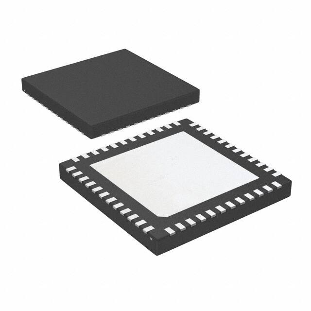


 工商网监
湘ICP备2023018690号
工商网监
湘ICP备2023018690号
