Preface
SNAU203 – March 2017
LMK04616 Evaluation Module
Julian Hagedorn
Overview
The LMK04616EVM features LMK04616 ultra-low noise and low power JESD204B compliant Dual Loop
Jitter Cleaner. With a power consumption of only 1200 mW with all outputs running, LMK04616 supports
65-fs jitter (12 kHz to 20 MHz) using a low-noise VCXO module. Integrated LDOs provide high PSRR that
enables the use of DC-DC converters.
The dual loop architecture consists of two high-performance phase-locked loops (PLL), a low-noise crystal
oscillator circuit, and a high-performance voltage controlled oscillator (VCO). The first PLL (PLL1) provides
a low-noise jitter cleaner function while the second PLL (PLL2) performs the clock and SYSREF
generation. PLL1 can be configured to either work with an external VCXO module or the integrated crystal
oscillator with an external tunable crystal and varactor diode. When used with a very narrow loop
bandwidth, PLL1 uses the superior close-in phase noise (offsets below 50 kHz) of the VCXO module or
the tunable crystal to clean the input clock. The output of PLL1 is used as the clean input reference to
PLL2 where it locks the integrated VCO. The loop bandwidth of PLL2 can be optimized to clean the far-out
phase noise (offsets above 50 kHz) where the integrated VCO outperforms the VCXO module or tunable
crystal used in PLL1.
Features
•
•
•
•
•
Dual Loop Architecture with typical 60-fs rms from 10 kHz to 20 MHz at 122.88-MHz output frequency
1.2-W typical power consumption for 16 outputs at 122.88 MHz
JEDEC JESD204B Support
Jumper configurable supplies with onboard LDOs and DCDC converters
GUI platform for full access to device registers
SNAU203 – March 2017
Submit Documentation Feedback
LMK04616 Evaluation Module
Copyright © 2017, Texas Instruments Incorporated
1
�SNAU203 – March 2017
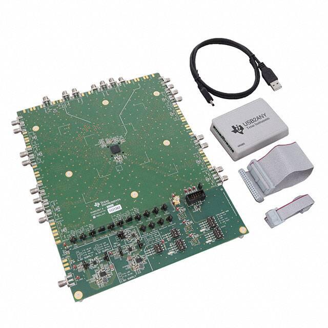
Quick Start Guide
Figure 1. LMK04616 EVM Quick Start Connection
1
Quick Start Description
The LMK04616 EVM allows full verification of the device functionality and performance specification. To
quickly set up and operate the board with basic equipment, refer to the quick start procedure below and
test setup shown in Figure 1.
2
LMK04616 Evaluation Module
SNAU203 – March 2017
Submit Documentation Feedback
Copyright © 2017, Texas Instruments Incorporated
�1.2 Device Start-Up Sequence
www.ti.com
1. Place Dip switches S1 to S5 into default position as shown in Table 5
2. Connect a supply voltage of 5 V to the VCC SMA.
3. Connect a reference clock to the CLKin1 port from a signal generator or other source. Use 122.88 MHz
for default.
4. Connect the SPI header to a computer using USB2ANY.
5. Program the device with TICS Pro.
(a) Start TICS Pro
(b) Select LMK04616 from Select device → Clock Generator/Jitter Cleaner (Dual Loop) → LMK0461x
Menu.
(c) Select from USB Communications → Interface Menu USB2ANY.
(d) Select default mode from the “Default Configuration” Menu. For the quick start use Dual Loop:
PLL1 BW= 40Hz REF: CLKin1 (single-ended)
(e) Ctrl-L must be pressed at least once to load all registers. Alternatively click menu Keyboard
Controls → Load Device.
(f) Click Device Start button in the Generic page or use the Device: DEV_STARTUP button from the
Tool bar.
6. Measurements may be made at an active CLKout port through its SMA connector.
2
1.2 Device Start-Up Sequence
All Supplies
powered up
Power Supplies
all off
DEVICE
NOT READY
Ramp-up Power Supplies
DEVICE IDLE
In
Power-Down
State
Release RESETn
RESETn = 0
(Power-down)
RESETn = X
(Power-down)
DEVICE IDLE
READY FOR SPI
PROGRAMMING
RESETn = 1
Program device configuration settings
DEVICE IDLE
DEVICE
CONFIG
PROGRAMMING
DONE
Trigger Startup
Sequence through SPI
DEV_STARTUP = 1
(self clearing bit)
RESETn = 1
DEVICE
BOOTING
UP
DEVICE
RUNNING
RESETn = 1
RESETn = 1
STAT0/1
indicates
PLL Lock
Figure 2. Device Start-Up Sequence
SNAU203 – March 2017
Submit Documentation Feedback
LMK04616 Evaluation Module
Copyright © 2017, Texas Instruments Incorporated
3
�SNAU203 – March 2017
Installing the EVM Control Software
1. Install latest TICS Pro software from web: http://www.ti.com/tool/ticspro-sw
2. Start TICS Pro.
3. Select Device → Clock Generator/Jitter Cleaner (Dual Loop) → LMK0461x → LMK04616
4
LMK04616 Evaluation Module
SNAU203 – March 2017
Submit Documentation Feedback
Copyright © 2017, Texas Instruments Incorporated
�SNAU203 – March 2017
Using the EVM Control Software
1
Keyboard Shortcuts
CTRL + L => write all registers
2
TICS Pro Overview
Figure 3. TICS Pro Overview
SNAU203 – March 2017
Submit Documentation Feedback
LMK04616 Evaluation Module
Copyright © 2017, Texas Instruments Incorporated
5
�TICS Pro With LMK04616 GUI Loaded
www.ti.com
Figure 4. TICS Pro User Manual
Further information at Help → TICS Pro User Manual
3
TICS Pro With LMK04616 GUI Loaded
Figure 5. TICS Pro With LMK04616 GUI Loaded
6
LMK04616 Evaluation Module
SNAU203 – March 2017
Submit Documentation Feedback
Copyright © 2017, Texas Instruments Incorporated
�GUI: Generic Control
www.ti.com
4
GUI: Generic Control
Figure 6. GUI: Generic Control
SNAU203 – March 2017
Submit Documentation Feedback
LMK04616 Evaluation Module
Copyright © 2017, Texas Instruments Incorporated
7
�GUI: Operating Modes
5
www.ti.com
GUI: Operating Modes
Figure 7. GUI: Operating Modes
8
LMK04616 Evaluation Module
SNAU203 – March 2017
Submit Documentation Feedback
Copyright © 2017, Texas Instruments Incorporated
�GUI: OSCin and OSCout
www.ti.com
6
GUI: OSCin and OSCout
Figure 8. GUI: OSCin and OSCout
7
GUI: LOS Control
Figure 9. GUI: LOS Control
SNAU203 – March 2017
Submit Documentation Feedback
LMK04616 Evaluation Module
Copyright © 2017, Texas Instruments Incorporated
9
�GUI: Holdover Control
8
www.ti.com
GUI: Holdover Control
Figure 10. GUI: Holdover Control
10
LMK04616 Evaluation Module
SNAU203 – March 2017
Submit Documentation Feedback
Copyright © 2017, Texas Instruments Incorporated
�GUI: Inputs and PLL1
www.ti.com
9
GUI: Inputs and PLL1
Figure 11. GUI: Inputs and PLL1
SNAU203 – March 2017
Submit Documentation Feedback
LMK04616 Evaluation Module
Copyright © 2017, Texas Instruments Incorporated
11
�GUI: PLL2
10
www.ti.com
GUI: PLL2
Figure 12. GUI: PLL2
12
LMK04616 Evaluation Module
SNAU203 – March 2017
Submit Documentation Feedback
Copyright © 2017, Texas Instruments Incorporated
�GUI: Outputs
www.ti.com
11
GUI: Outputs
Figure 13. GUI: Outputs
SNAU203 – March 2017
Submit Documentation Feedback
LMK04616 Evaluation Module
Copyright © 2017, Texas Instruments Incorporated
13
�GUI: EVM
12
www.ti.com
GUI: EVM
Figure 14. GUI: EVM Overview
14
LMK04616 Evaluation Module
SNAU203 – March 2017
Submit Documentation Feedback
Copyright © 2017, Texas Instruments Incorporated
�SNAU203 – March 2017
Configuring the Board
The LMK04616 is a programmable clock jitter cleaner with many options. The EVM was designed with
maximum flexibility so engineers can configure the EVM for operation at its desired mode.
Figure 15 shows the connection concept of the LMK04616EVM.
VDD
VCXO
VDD
3V3 Plane
Direct
LDO
DC/DC
options
1V8 Plane
VCXO LDO
Power distribution
jumpers
LMK04616
144 pin BGA
Output interface
OUT0
Output interface
OUT15
Output interface
OSCout
Vctrl
Filter
placeholder
VCXO
Input
interface
OSCin
External
VCXO
CLKin0
Input interface
CLKin3
Input interface
Logic I/O
interface
U2A connector
Copyright © 2017, Texas Instruments Incorporated
Figure 15. EVM Connection Concept
1
Configuring the Power Supply
Figure 16 shows the default jumper setting to supply 3.3 V and 1.8 V to the device.
The VDD SMA or VDD_2 terminal block (on the back side of the EVM) is connected to J1 and J5 to
provide the external supply voltage for the 3.3-V and 1.8-V supply plane.
The VDD_VCXO SMA is directly connected to the VCXO LDO.
SNAU203 – March 2017
Submit Documentation Feedback
LMK04616 Evaluation Module
Copyright © 2017, Texas Instruments Incorporated
15
�Configuring the Power Supply
www.ti.com
Figure 16. Default Power Supply Connection
1.1
Supply Plane Source Selection
Jumper J1 and J2 selects the Power connection for the 3.3-V plane from either the LDO, a DC-DC
switcher or direct from VDD SMA Connector.
16
LMK04616 Evaluation Module
SNAU203 – March 2017
Submit Documentation Feedback
Copyright © 2017, Texas Instruments Incorporated
�Configuring the Power Supply
www.ti.com
Table 1. 3.3-V Supply Plane Connections
DESCRIPTION
JUMPER SETTING
3.3-V LDO
(TPS7A8101)
J1: 1-2
J2: 2-3
3.3-V DC-DC
(TPS54120)
J1: 2-3
J2: 1-2
SNAU203 – March 2017
Submit Documentation Feedback
PICTURE
LMK04616 Evaluation Module
Copyright © 2017, Texas Instruments Incorporated
17
�Configuring the Power Supply
www.ti.com
Table 1. 3.3-V Supply Plane Connections (continued)
DESCRIPTION
JUMPER SETTING
Direct from VDD SMA
NOTE: Apply 3.3 V only!
J1: 2-4
J2: 2-4
PICTURE
Jumper J6 and J5 selects the Power connection for the 1.8-V plane from either a LDO or a DC-DC
switcher.
Table 2. 1.8-V Supply Plane Connections
18
DESCRIPTION
JUMPER SETTING
1.8-V LDO
(TPS7A8101)
J5: 1-2
J6: 2-3
1.8 V DC/DC
(TPS54120)
J5: 2-3
J6: 1-2
LMK04616 Evaluation Module
PICTURE
SNAU203 – March 2017
Submit Documentation Feedback
Copyright © 2017, Texas Instruments Incorporated
�Configuring the Power Supply
www.ti.com
Table 2. 1.8-V Supply Plane Connections (continued)
DESCRIPTION
JUMPER SETTING
Adjustable DC-DC
(TPS62150)
J5: 2-4
J6: open
PICTURE
J7 sets the output voltage for the adjustable DC-DC plane.
Table 3. Adjustable DC-DC Supply Settings
DESCRIPTION
JUMPER SETTING
3.3-V output voltage
J5: 2-4
J7: bottom
2.5-V output voltage
J5: 2-4
J7: middle
1.8-V output voltage
J5: 2-4
J7: Top
SNAU203 – March 2017
Submit Documentation Feedback
PICTURE
LMK04616 Evaluation Module
Copyright © 2017, Texas Instruments Incorporated
19
�Configuring the Power Supply
1.2
www.ti.com
Power Distribution
The power distribution jumpers (J9, J11, J12, J14, J16, J17, J19, J21, J22, J24, J25, J27, J29, J34 and
J36) are connected to the 3.3-V and 1.8-V supply planes and individual external connections.
Figure 17. Power Distribution Jumpers
J17 (VDD_CORE) and J24 (VDD_PLL2_OSC) selects between 3.3-V supply plane and adjustable DC-DC
connection as shown in Figure 18.
Figure 18. J17, J24 Connection Description
J21 (VDD_PLL1) selects between 3.3-V supply plane, VCXO LDO and adjustable DC-DC connection as
shown in Figure 19.
Figure 19. J21 Connection Description
J9 (VDDO_89), J11 (VDD_IO), J12 (VDDO_1011), J14 (VDD_OSC), J16 (VDD_PLL2OSC), J19
(VDDO_67), J22 (VDDO_01), J25 (VDDO_23), J27 (VDDO_45), J34 (VDDO_1213) and J36
(VDDO_1415) selects between 3.3-V supply plane, 1.8-V supply plane and adjustable DC-DC connection
as shown in Figure 20.
Figure 20. J9, J11, J12, J14, J16, J19, J22, J25, J27, J34, J36 Connection Description
20
LMK04616 Evaluation Module
SNAU203 – March 2017
Submit Documentation Feedback
Copyright © 2017, Texas Instruments Incorporated
�Configuring the Power Supply
www.ti.com
1.3
VCXO Supply Connection
The VCXO has its own LDO (LM5907MFX-3.3). A 5-V supply needs to be connected to VCC_VCXO
SMA. Jumper J29 selects between this LDO, the LMK04616 3.3-V supply plane and an adjustable DC-DC
supply connection as shown inTable 4.
Table 4. VCXO Supply Connections
2
DESCRIPTION
JUMPER SETTING
3.3-V LDO
(LM5907MFX-3.3)
J26: 2-4
3.3-V supply plane
(TPS7A8101 or TPS54120)
J26: 2-3
Adjustable DC-DC supply
connection on Jumper J28
(TPS62150)
NOTE: Apply 3.3 V only!
J26: 1-2
PICTURE
Dip Switch Configuration
Default configuration of Dip Switches is shown in Table 5 or Figure 21.
Table 5. Default Dip Switch Configuration
SWITCH POSITION S2 SYNC/SYSREF
REQ
S3 STAT0
S4 SDIO
S5 STAT1
S6 CLKin_SEL
1 – High
OFF
OFF
OFF
OFF
OFF
2 – U2A
ON
ON
ON
ON
ON
3 – Low
OFF
OFF
OFF
OFF
OFF
4 – LED
ON
ON
n/a
ON
n/a
SNAU203 – March 2017
Submit Documentation Feedback
LMK04616 Evaluation Module
Copyright © 2017, Texas Instruments Incorporated
21
�Dip Switch Configuration
www.ti.com
Figure 21. Default Dip Switch Setting
22
LMK04616 Evaluation Module
SNAU203 – March 2017
Submit Documentation Feedback
Copyright © 2017, Texas Instruments Incorporated
�SNAU203 – March 2017
LMK04616 EVM Board Schematic
SNAU203 – March 2017
Submit Documentation Feedback
LMK04616 Evaluation Module
Copyright © 2017, Texas Instruments Incorporated
23
�www.ti.com
L14
U11
3V3 LDO option
C163
10µF
R1
U5
7
8
R199
IN
IN
5
EN
Label
5V : LDO/DC
3.3V : Direct
R198
30.9k
Ra
9
4
9
GND
PVIN
PVIN
AVIN
Bypassing for 3V3 Plane
R200
10.0k
Vout = 0.8 * (1 + Ra/Rb)
Vout=1.8V : Ra=12.5k, Rb=10k
Vout=3.3V : Ra=30.9k, Rb=10k
TPS7A8101DRBT
R4 0
R5
populate if common bypass is needed
0
8
7
1
2
3
SW
SW
SW
EN
SS/TR
C164
22µF
R3
4
PG
100k
5
FB
GND
17
6
15
16
EP
AGND
PGND
PGND
DEF
FSW
adj. DC/DC
2.2µH
14
VOS
3300pF
C88
10µF
C90 Rb
0.47µF
13
0 C165
C87
0.47µF
GND
C89
10µF
R2
1.0k
3
6
FB
NR
5.1k
Label
2-1 : LDO
2-4 : Direct
2-3 : DC/DC
1
2
OUT
OUT
11
12
10
TPS62150RGTR
VDD_3V3_PLANE
J1
1
2
3
1
J2
4 Put corresponding 4-way jumpers close GND
1
J3
TSW-103-07-G-S
2
3
4
5
3
2
1
1
C91
0.1µF
TSW-103-07-G-S
142-0701-806
C95
10µF
C96
0.1µF
default placement for
this shunts is 2-3
C97
47µF
C98
R201
100pF 41.2k
GND
SH-J2
U6
16
17
C99
0.1µF
39357-0002
18
PH
PH
LDOIN
LDOIN
LDOEN
BOOT
VSENSE
11
GND
put on the back side
GND
GND
C93
1µF
1.8V
GND
SH1
SH-J1
9
10
C100
10µF
15
GND
R207
C108
6
100k
14
0.01µF
GND
13
R210
2.2k
19
5
20
C110
C111
0.33µF
0.047µF
1
3
5
23
24
21
12
GND
C94
0.1µF
GND
R202
2.5V
3.3V
R6
249k
R7
422k
R8
619k
R10
200k
R12
200k
R13
200k
2
4
6
J7
R203
10.0k
0
1V8 LDO option
U7
VIN
PVIN
PVIN
OUT
OUT
R205
EN
Ra
FB
7
8
GND
1
2
3
R206
30.9k
C102
0.1µF
C103
10µF
C104
100µF
RT/CLK
SS
NR
Rb
DAP
PGND
PGND
GND
NC
NC
EN
GND
Ra
R204
12.4k
C107 Rb
0.47µF
R208
10.0k
3
6
FB
NR
5.1k
C101
0.47µF
GND
GND
default placement for
this shunts is 1-2
C105
10µF
GND
C106
10µF
Label
2-1 : LDO
2-3 : DC/DC
2-4 : adj. DC/DC
1
2
OUT
OUT
Bypassing for 1V8 Plane
populate if common bypass is needed
TPS7A8101DRBT
22
COMP
PWRGD
5
IN
IN
4
1
2
C92
10µF
GND
default placement for
this shunts is 1-2
VDD_1
DC/DC__DUT__Power
220 ohm
J4
L1
744031220
TP_1
VDD_3V3_PLANE
FB1
9
TP_VDD1
VDD
VDD1
25
7
8
4
R209
10.0k
see 3V3 LDO for Vout formula
J5
Vout = 0.8 * (1 + Ra/Rb)
Vout=1.8V : Ra=12.5k, Rb=10k
Vout=3.3V : Ra=30.9k, Rb=10k
C109
0.1µF
J6
GND
1
2
3
SH-J3
3
2
1
1
J8
TSW-103-07-G-S Put corresponding 4-way jumpers close
FB2
TP9
VDD_1V8_PLANE
VDD_1V8_PLANE
220 ohm
TSW-103-07-G-S
C112
0.1µF
C113
10µF
C114
1µF
C115
0.1µF
TPS54120RGYR
Floating EN = Enabled
GND
GND
GND
GND
3V3 DC/DC option
SH-J4
LDO is used
default placement for
this shunts is 2-3
16
17
18
11
VCC_VCXO_LDO
1
2
3
4
5
R215
C124
1µF
5.1k
3
4
VIN
VOUT
15
5
GND
EN
N/C
GND
9
10
C122
10µF
TP10
VCC_VCXO_LDO
U9
1
2
C123
C125
1µF
R216
100k
19
GND
GND
14
13
R217
2.2k
GND
6
0.01µF
GND
LP5907MFX-3.3/NOPB
GND
C119
100µF
C128
0.047µF
GND
GND
GND
GND
C120 R211
100pF 12.4k
PH
PH
LDOIN
LDOIN
LDOEN
BOOT
VSENSE
VCC_VCXO1
C118
47µF
GND
R214
0
142-0701-806
C117
0.1µF
U8
C121
0.1µF
DNP
C116
10µF
L2
744031220
C127
0.33µF
5
20
GND
23
24
21
12
R212
GND
5.1k
R213
10.0k
see 3V3 DC/DC for Vout formula
VIN
PVIN
PVIN
OUT
OUT
GND
1
2
EN
FB
3
RT/CLK
SS
NR
22
COMP
PWRGD
NC
NC
DAP
PGND
PGND
GND
25
7
8
4
C126
0.1µF
TPS54120RGYR
VCXO LDO option
Floating EN = Enabled
GND
GND
GND
1V8 DC/DC option
LDO is not used
Copyright © 2017, Texas Instruments Incorporated
Figure 22. Power Supply Connection
24
LMK04616 Evaluation Module
SNAU203 – March 2017
Submit Documentation Feedback
Copyright © 2017, Texas Instruments Incorporated
�www.ti.com
default placement for
this shunt is 2-4
J9
4
adj. DC/DC
1
2
3
1
J10
L15
R14
220 ohm
0
C166
0.1µF
TSW-103-07-G-S
SH-J81
default placement for
this shunt is 2-4
C168
0.1µF
C167
1µF
GND
VDDO_8_9
GND
Supply Selection and Bypassing
GND
Label
2-1 : adj DCDC
2-3 : 3V3
2-4 : 1V8
default placement for
this shunt is 2-4
J12
4
1
2
3
1
SH-J82
J33
L16
R15
220 ohm
0
C169
0.1µF
TSW-103-07-G-S
VDD_1V8_PLANE
C170
1µF
GND
default placement for
this shunt is 2-4
VDDO_10_11
C171
0.1µF
GND
J11
4
SH-J5
GND
J13
TSW-103-07-G-S
1
2
3
L17
1
2
3
GND
TSW-103-07-G-S
VDDO_14_15
default placement for
this shunt is 2-3
0
C177
0.1µF
GND
4
GND
default placement for
this shunt is 2-4
TSW-103-07-G-S
VDD_CORE_LOGIC
L6
R221
220 ohm
0
C138
0.1µF
C139
10µF
SH-J9
VDD_CORE
4
SH-J10
GND
Label
2-1 : adj DCDC
2-3 : 3V3
2-4 : LDO
C133
10µF
GND
C134
0.1µF
VDD_OSC
replace 0 Ohm with ferrite bead in
case required to place it closer to
the device
GND
L5
R220
220 ohm
0
C136
10µF
GND
J20
VDD_1V8_PLANE
C140
0.1µF
TSW-103-07-G-S
GND
GND
GND
VDD_PLL2_CORE
C137
0.1µF
GND
4
TSW-103-07-G-S
L8
R223
220 ohm
0
C144
0.1µF
C145
10µF
TSW-103-07-G-S
VDD_PLL1
default placement for
this shunt is 2-4
C146
0.1µF
GND
4
GND
TSW-103-07-G-S
Label
2-1 : adj DCDC
2-3 : 3V3
L10
R225
220 ohm
0
C150
0.1µF
C151
10µF
default placement for
this shunt is 2-4
VDD_PLL2_OSC
GND
R224
0
C148
1µF
GND
VDDO_0_1
C149
0.1µF
GND
L11
R226
220 ohm
0
C153
0.1µF
C154
1µF
GND
GND
VDDO_2_3
C155
0.1µF
GND
J27
4
SH-J14
1
2
3
1
C152
0.1µF
J28
TSW-103-07-G-S
GND
GND
220 ohm
GND
1
2
3
TSW-103-07-G-S
J24
1
2
3
GND
C143
0.1µF
L9
C147
0.1µF
J26
default placement for
this shunt is 2-3
SH-J13
C142
1µF
VDDO_6_7
J25
SH-J12
1
GND
0
GND
J23
J31
R222
220 ohm
C141
0.1µF
1
2
3
1
1
2
3
L7
J22
SH-J11
J21
4
0
C135
0.1µF
1
2
3
1
default placement for
this shunt is 2-4
1
R219
J19
J17
1
2
3
default placement for
this shunt is 2-3
GND
220 ohm
GND
J18
Label
2-1 : adj DCDC
2-3 : 3V3
SH-J8
GND
C131
0.1µF
L4
C132
0.1µF
1
2
3
TSW-103-07-G-S
default placement for
this shunt is 2-3
C130
10µF
VDD_IO
J16
SH-J7
1
GND
0
GND
1
2
3
1
GND
C176
1µF
R218
220 ohm
C129
0.1µF
J15
220 ohm
L3
J14
4
SH-J6
R17
C175
0.1µF
TSW-103-07-G-S
default placement for
this shunt is 2-4
C174
0.1µF
L18
J37
SH-J84
C173
1µF
GND
J36
4
1
VDDO_12_13
0
C172
0.1µF
TSW-103-07-G-S
default placement for
this shunt is 2-4
R16
220 ohm
J35
SH-J83
1
2
3
1
J34
4
1
All 0.1uF Bypass caps to be placed
close to the LMK045XX device
supply pin.
adj. DC/DC
GND
VDD_3V3_PLANE
Label
2-1 : open
2-3 : 3V3
2-4 : LDO
default placement for
this shunt is 2-4
L12
R227
220 ohm
0
C156
0.1µF
C157
1µF
GND
GND
VDDO_4_5
C158
0.1µF
GND
Keep the GND_VCXO close to the VCXO island, move
bypass group closer to VCXO
J29
VCC_VCXO_LDO
SH-J15
4
1
1
2
3
TSW-103-07-G-S
Bypass
In case multiple pins are to be supplied directly from a VDD plane (3V3 or 1V8), 10uF,s1uF
can cap
be
omitted and the ferrite bead can be replaced by a 0-Ohm resistor. the plance bypass/
decoupling scheme
should be used instead in this case.
VCC_VCXO
L13
220 ohm
J30
C159
0.1µF
C160
10µF
C161
0.1µF
C162
100pF
GND
GND_VCXO
Place the 0.1uF cap as close as possible to the DUT
Copyright © 2017, Texas Instruments Incorporated
Figure 23. Power Distribution
SNAU203 – March 2017
Submit Documentation Feedback
LMK04616 Evaluation Module
Copyright © 2017, Texas Instruments Incorporated
25
�www.ti.com
Pin 3 is SPI readback
for 3-level inputs
referred to internal 2.5V
VDD_1V8_PLANE
High Level (min): 0.77 V
Mid level : 0.52 V (0.21x2.5V)
Low Level (max) : 0.4 V (0.16 x 2.5V)
VDD_1V8_PLANE
U2A_STAT0
U2A_CLKIN_SEL
U2A_SCL
U2A_RESETN
GND
VDD_3V3_PLANE
9
7
5
3
1
1
2
R230
52601-S10-8LF
U2A_SDIO
VCCA
U2A_SCSN
3
VCCB
A1
B1
A2
B2
8
6
U2A_SYNC
GND
R232
4.7k
U2A_STAT1
7
1.0k
1
2
3
4
R61
GND
R231
1
10
8
6
4
2
R59
4.7k
U2A_SYNC R60
4.7k
U10
JU1
5
DIR
GND
GND
4
2
1.0k
CAVC2T45TDCURQ1
64 KOhm pull up/pull down at input
8
7
6
5
so mid level is designed to be
0.184 x 3.3V
219-4LPST
R229
270
1.0k
S2
D3
LTST-C150CKT
R63
Red
0
GND
SPI_SCSN
R233
4.7k
TP2
SYNC
SYNC/SYSREF REQ
GND
1
TP1
SPI_SCSN
U2A_SCSN R62
4.7k
C47
100pF
SYNC
2
3
4
5
GND
GND
C48
100pF
5-1814832-1
GND
GND
unidirectional signals
VDD_1V8_PLANE
RESETN
CLKIN_SEL
SCSN
SCL
R228
21.0k
VDD_1V8_PLANE
all other signals are
bidirectional
R64
J32
SH-J16
1
2
TP3
RESETN
R67
TSW-102-07-G-S
R68
4.7k
R234
4.7k
1
RESETN
4.7k
C49
100pF
GND
8
7
6
5
U2A_SCL
TP5
STATUS0
STAT0
GND
1
2
3
4
5
- Route all bidirectional outputs
[SYNC, STATUS0/1, SDIO] as
50-Ohm single ended RF trace to
SMA
- use suffecient clearance between
individual birectional outputs and the
other RF outputs.
GND
SPI_SCL
R235
4.7k
C51
100pF
GND
VDD_1V8_PLANE
R72
4.7k
1
1
2
3
4
4.7k
U2A_STAT1 R75
4.7k
6
219-3LPST
U2A_CLKIN_SEL R82
4.7k
2
5
CLKIN_SEL
219-3LPST
3
3-level input
VDD, 0.18 VDD, and
GND
A : VDD
AC : 0.18 VDD
C : GND
B : U2A control
S6B
TP6
CLKIN_SEL
S6C
4
C52
100pF
1
4.7k
GND
GND
SDIO_out
1
R83
0
3 level static input
U2A input
LED output indicator
optional out SMA
S4B
5
219-3LPST
3
S4C
4
219-3LPST
R81
0
DNP
GND
6
GND
TP7
STATUS1
5-1814832-1
219-3LPST
R78
D2
R80
LTST-C150CKT
0
Red
STAT1
2
4.7k
1
GND
2
1
4.7k
S6A
2
3
4
5
R79
4.7k
R74
U2A_SDIO
R76 219-4LPST
270
R77
S4A
219-3LPST
8
7
6
5
C53
100pF
STATUS1
TP8
SPI_SDIO
R84
0
DNP
2
3
4
5
VDD_1V8_PLANE
S5
GND
STATUS0
VDD_1V8_PLANE
R73
C50
100pF
GND
R71
0
DNP
5-1814832-1
TP4
SPI_SCL
R69
4.7k
D1
R70
LTST-C150CKT
0
Red
GND
GND
S3
R66 219-4LPST
270
2
U2A_RESETN
1
2
3
4
4.7k
U2A_STAT0 R65
4.7k
5-1814832-1
GND
GND
SPI_SDIO
C54
100pF
Bidirectional
GND
R85
4.7k
Copyright © 2017, Texas Instruments Incorporated
GND
Figure 24. Logic
26
LMK04616 Evaluation Module
SNAU203 – March 2017
Submit Documentation Feedback
Copyright © 2017, Texas Instruments Incorporated
�www.ti.com
CLKIN0_P
CLKIN0_N
H12
H11
CLKIN1_P
CLKIN1_N
J12
K12
CLKIN2_P
CLKIN2_N
L12
M12
CLKIN3_P
CLKIN3_N
G10
CLKIN_SEL
G1
G2
SPI_SCL
SPI_SDIO
H2
SPI_SCSN
C33
33pF
GND
C34
33pF
GND
RESETN
C35
33pF
SYNC
OSCOUT_P
OSCOUT_N
D12
E12
D10
PLL1_CAP
E9
PLL2_LDO_CAP
PLL2_VCOLDO_CAP
R49
0
R50
0
CLKOUT2P
CLKOUT2N
CLKIN3P
CLKIN3N
CLKOUT3P
CLKOUT3N
CLKIN_SEL
CLKOUT4P
CLKOUT4N
SCL
SDIO
F4
E4
PLL2_VCOCAP_BASE D5
CLKOUT5P
CLKOUT5N
SCS
SYNC/SYSREF_REQ
B12
OSCIN_N
CLKIN2P
CLKIN2N
RESET
A12
OSCIN_P
CLKOUT1P
CLKOUT1N
J2
F1
STATUS1
CLKOUT0P
CLKOUT0N
CLKIN1P
CLKIN1N
H1
E1
STATUS0
GND
placeholder, don't populate caps by default
CLKIN0P
CLKIN0N
CLKOUT6P
CLKOUT6N
CLKOUT7P
CLKOUT7N
STATUS0
STATUS1
CLKOUT8P
CLKOUT8N
OSCINP
CLKOUT9P
CLKOUT9N
OSCINN
CLKOUT10P
CLKOUT10N
OSCOUTP
CLKOUT11P
CLKOUT11N
OSCOUTN
CTRL_VCXO
CLKOUT12P
CLKOUT12N
PLL1_CAP
CLKOUT13P
CLKOUT13N
PLL2_LDO_CAP
CLKOUT14P
CLKOUT14N
PLL2_VCOLDO_CAP
CLKOUT15P
CLKOUT15N
NC
NC
PLL2_VCOCAP_ BASE
CLKOUT0_P
CLKOUT0_N
L1
M1
R47
OSCOUT_N
CLKOUT2_P
CLKOUT2_N
L4
M4
C37
10µF
GND
C38
10µF
GND
C39 DNPC40
10µF
10µF
GND
GND
GND
C32
OSCO_N
GND
OSCOUT_N
OSCO1_N
DNP
1
DNP
0.1µF
R48
51
Apply output layout guidelines on OSCOUT
OSCOUT supports LVDS/HSDS/HCSL/LVCMOS
CLKOUT4_P
CLKOUT4_N
L7
M7
1
142-0701-806
0
142-0701-806
GND
GND
CLKOUT5_P
CLKOUT5_N
M9
L9
All three VCXOs should share the same footprint.
VG-4513CB is 7x5mm
VG-4513CA is 5x3mm, should be placed within
the above footprint, it has different pin spacing
CVHD-950-4 is 4 pin part, but has 200 mil
spacing, so it's compatible with the 6 pin
components above. with the following pin
mapping
CVHD-950-4
VG-4513CB
1
1
2
3
3
4
4
6
CLKOUT6_P
CLKOUT6_N
L10
M10
CLKOUT7_P
CLKOUT7_N
A10
B10
CLKOUT8_P
CLKOUT8_N
A9
B9
CLKOUT9_P
CLKOUT9_N
B7
A7
CLKOUT10_P
CLKOUT10_N
B6
A6
CLKOUT11_P
CLKOUT11_N
B4
A4
CLKOUT12_P
CLKOUT12_N
B3
A3
U2
3
CLKOUT13_P
CLKOUT13_N
B1
A1
VCC
4
5
6
5.0x3.2 mm
VG-4513CA-122.8800M-GFCT3
122.88 MHz
C36
DNP
0.01µF
NC1
U3
NC2
GND
OUT-
VC
CLKOUT15_P
CLKOUT15_N
R53
DNP
0
OUT+
DNP
OE
1
CLKOUT14_P
CLKOUT14_N
D1
C1
GND
2
3
LMK04616ZCR
DUT ground pad:
- No SOLDERMASK on bottom thermal pad,
exposed copper
- use via array with
0.3mm hole, 0.5mm via diameter,
0.8mm via pitch
- ground floor on all layers except split power
plane
0.1µF
CLKOUT3_P
CLKOUT3_N
L6
M6
OSCO1_P
R45
DNP
51
R46
DNP
100
CLKOUT1_P
CLKOUT1_N
L3
M3
D3
D4
OSCO_P
0
J1
K1
OSCOUT_P
C31
R44
OSCOUT_P
U1A
G12
G11
R51
120 FB
R54
DNP
0
R52
0
GND
2
1
VC
OUTVCC
4
VCXO_OUT_P
5
VCXO_OUT_N
6
7.0x5.0 mm
VG-4513CB-122.8800M-GFCT3
122.88 MHz
GND_VCXO
GND
OUT+
DNP
OE
U4
6
C41
100pF
1
2
GND_VCXO
VDD
VCONT
OUT
COUT
E/D
GND
4
VCC_VCXO
5
3
14.2x9.14 mm
603281
122.88MHz
Y1
CTRL_VCXO
S1A
S1B
R56
R57
0
0
DNPC42
0.1µF
C44
1µF
C45
4.7µF
C46
10µF
GND
DNP
R58
DNP
0
S1C
DNPC43
0.1µF
VCTRL
1
R55
DNP
0
DNP
5-1814832-1
GND
use for external VCXO
This filter is a placeholder.
by default it's not used, however
3rd order pole can be used.
VG2520CAN61.440000MHZCJGNBB
61.44 MHz
Please check feasibility of overlaying this smaller
VCXO with other 3. the above 3 are possible.
Copyright © 2017, Texas Instruments Incorporated
Figure 25. LMK04616 Main Connection
SNAU203 – March 2017
Submit Documentation Feedback
LMK04616 Evaluation Module
Copyright © 2017, Texas Instruments Incorporated
27
�www.ti.com
U1B
VDD_IO
H10
VDD_OSC
E11
VDD_CORE
H4
VDDO_0_1
K2
VDDO_2_3
K5
VDDO_4_5
K8
VDDO_6_7
K10
VDDO_8_9
C10
VDDO_10_11
C8
VDDO_12_13
C5
VDDO_14_15
C2
VDD_PLL1
F9
VDD_PLL2_OSC
E3
VDD_PLL2_CORE
G3
A2
A5
A8
A11
B2
B5
B8
B11
C3
C4
C6
C7
C9
C11
C12
D2
D6
D7
D8
D9
D11
VDD_IO
VDD_OSC
VDD_CORE
VDDO0/1
VDDO2/3
VDDO4/5
VDDO_6/7
VDDO_8/9
VDDO10/11
VDDO12/13
VDDO14/15
VDDPLL1
VDD_PLL2_OSC
VDD_PLL2_CORE
VSS
VSS
VSS
VSS
VSS
VSS
VSS
VSS
VSS
VSS
VSS
VSS
VSS
VSS
VSS
VSS
VSS
VSS
VSS
VSS
VSS
VSS
VSS
VSS
VSS
VSS
VSS
VSS
VSS
VSS
VSS
VSS
VSS
VSS
VSS
VSS
VSS
VSS
VSS
VSS
VSS
VSS
VSS
VSS
VSS
VSS
VSS
VSS
VSS
VSS
VSS
VSS
VSS
VSS
VSS
VSS
VSS
VSS
VSS
VSS
VSS
VSS
VSS
VSS
VSS
VSS
VSS
VSS
VSS
VSS
VSS
E2
E5
E6
E7
E8
E10
F2
F3
F5
F6
F7
F8
F10
F11
F12
G4
G5
G6
G7
G8
G9
H3
H5
H6
H7
H8
H9
J3
J4
J5
J6
J7
J8
J9
J10
J11
K3
K4
K6
K7
K9
K11
L2
L5
L8
L11
M2
M5
M8
M11
LMK04616ZCR
GND
GND
Copyright © 2017, Texas Instruments Incorporated
Figure 26. LMK04610 Power Connection
28
LMK04616 Evaluation Module
SNAU203 – March 2017
Submit Documentation Feedback
Copyright © 2017, Texas Instruments Incorporated
�www.ti.com
CLKIN1_P
C10
C3
CLKIN0_N
0.1µF
2
3
4
5
0.1µF
142-0701-806
CK1_P
CLKIN1_P
0.1µF
DNPC12
0.1µF
DNPC5
0.1µF
0.1µF
142-0701-806
R11
100
GND
C2
C1
1
CK0_N
1
2
3
4
5
CLKIN0_N
R9
DNP
100
GND
GND
GND
CLKIN1_N
C9
C4
1
CK0_P
1
DNP
CLKIN0_P
0.1µF
2
3
4
5
0.1µF
DNP
CK1_N
DNP
0.1µF
CLKIN1_N
0.1µF
C11
0.1µF
2
3
4
5
CLKIN0_P
C8
C7
DNPC6
0.1µF
142-0701-806
142-0701-806
GND
GND
GND
GND
By default, CLKIN0 SMA is DC coupled to the 100
Ohm, then AC coupled to CLKIN0 input
CLKIN2_P
By default, CLKIN1 SMA is DC coupled to the 51
Ohm, then AC coupled to CLKIN1 input
CLKIN1 is single-ended by default (negative input
is connected to 0.1uA)
C13
C14
CK2_P
1
CLKIN3_P
CLKIN2_P
0.1µF
C16
C15
CK3_P
1
DNPC17
0.1µF
CLKIN3_P
0.1µF
0.1µF
2
3
4
5
2
3
4
5
0.1µF
142-0701-806
R26
100
GND
142-0701-806
GND
DNPC18
0.1µF
R27
DNP
100
GND
GND
CLKIN2_N
C19
C20
CK2_N
1
CLKIN3_N
CLKIN2_N
0.1µF
1
DNPC23
0.1µF
DNP
DNP
C22
CK3_N
0.1µF
DNP
CLKIN3_N
0.1µF
C24
0.1µF
2
3
4
5
2
3
4
5
0.1µF
C21
142-0701-806
142-0701-806
GND
GND
GND
GND
By default, CLKIN2 SMA is DC coupled to the 100
Ohm, then AC coupled to CLKIN2 input
OSCIN_P
1
R34
DNP
0
100/51 Ohm resistors can be used for
attenuation, otherwise replace by 0-Ohm
2
3
4
5
DNP
By default, CLKIN3 SMA is DC coupled to the 100
Ohm, then AC coupled to CLKIN3 input
5-1814832-1
GND
C25
VCXO_OUT_P
R36
120
0.1µF
1
DNPC27
0.1µF
GND
C28
0.1µF
R43
DNP
0
2
3
4
5
DNP
0.1µF
GND
GND
VCXO_OUT_N
OSCIN_N
R37
51
R39
DNP
100
0
R40
120
OSCIN_P
0
R38
CLOCK INPUT CLKIN0,CLKIN1 LAYOUT REQUIREMENTS:
∗∗∗ CONTROLLED IMPEDANCE ∗∗∗
- Route as 50-ohm (+/-5% tol.) controlled-impedance single-ended RF traces from SMA centerDUT
pin pin
to
- Place component pads directly on RF traces (no stubs), match 50-ohm trace width
A to
center
SM pad, and use 50-ohm Zo via structures.
∗∗∗ LENGTH / SKEW MATCHING ∗∗∗
- Equalize total path length and indiv. trace segments WITHIN pair from DUT to SMA
NOpins
INTRA-pair
(
skew).
- There is NO requirement to match inter-pair skew between CLKIN0 path and CLKIN1 path.
- Total path length should be as short as possible. Use 45 deg. serpentine pattern on stripline
internal only to equalize lengths within pair.
∗∗∗ SHIELDING / ISOLATION ∗∗∗
- Use ground shielding on routing layers with clearance to not affect controlled impedance
RF traces.
of
- Ground flood on routing layers should have clearance of more than 2.5x width from RF traces.
- Use ground stitching vias with 100 mil spacing around RF traces to connectertogeth
GND shielding on all layers.
- Avoid crossing Digital signal/return paths with REF input signal/return paths;
navoidable,
if u
cross at a 90 deg. angle
C26
R35
C29
R41
0
OSCIN_N
R42
51
GND
0.1µF
DNPC30
0.1µF
GND
5-1814832-1
GND
Apply Clock input layout guidelines on OSCIN
By default VCXO path (single ended) is AC coupled to OCSIN_P
Copyright © 2017, Texas Instruments Incorporated
Figure 27. Inputs
SNAU203 – March 2017
Submit Documentation Feedback
LMK04616 Evaluation Module
Copyright © 2017, Texas Instruments Incorporated
29
�www.ti.com
OUT0_P
O0_P
OUT0_P
CLKOUT4_P
5
4
3
2
R89
DNP
51
0.1µF
R92
DNP
100
OUT4_P
C56
1
142-0701-806
O4_P
Output interface supports
HSDS/LVDS (diff 100 Ohm)
HCSL (single ended 50 Ohm)
OUT4_P
DNP
R91
51
0.1µF
1
5
4
3
2
C55
CLKOUT0_P
R93
DNP
100
142-0701-806
GND
O0_N
R97
DNP
51
GND
C58
1
CLKOUT4_N
O4_N
500mil spacing for the P/N
SMA connectors
1
DNP
R99
51
0.1µF
142-0701-806
OUT4_N
OUT4_N
5
4
3
2
0.1µF
GND
OUT0_N
OUT0_N
5
4
3
2
GND
C57
CLKOUT0_N
142-0701-806
GND
GND
GND
GND
O1_P
OUT1_P
OUT5_P
C60
1
CLKOUT5_P
O5_P
DNP
OUT5_P
R105
DNP
51
0.1µF
5
4
3
2
R103
51
0.1µF
R106
DNP
100
R107
DNP
100
142-0701-806
1
5
4
3
2
OUT1_P
C59
CLKOUT1_P
142-0701-806
GND
O1_N
GND
C62
1
CLKOUT5_N
O5_N
DNP
OUT5_N
OUT5_N
R113
DNP
51
0.1µF
5
4
3
2
R111
51
0.1µF
GND
OUT1_N
OUT1_N
142-0701-806
1
5
4
3
2
GND
C61
CLKOUT1_N
142-0701-806
GND
GND
GND
GND
O2_P
OUT2_P
R117
DNP
51
OUT6_P
C64
1
CLKOUT6_P
O6_P
OUT6_P
R119
DNP
51
0.1µF
5
4
3
2
0.1µF
R120
DNP
100
R121
DNP
100
142-0701-806
1
5
4
3
2
OUT2_P
C63
CLKOUT2_P
142-0701-806
GND
O2_N
OUT2_N
R125
DNP
51
0.1µF
GND
GND
C66
1
CLKOUT6_N
O6_N
OUT6_N
OUT6_N
R127
DNP
51
0.1µF
5
4
3
2
CLKOUT2_N
OUT2_N
142-0701-806
1
5
4
3
2
GND
C65
142-0701-806
GND
GND
GND
GND
O3_P
OUT3_P
1
CLKOUT7_P
O7_P
DNP
R131
51
0.1µF
OUT7_P
R133
51
0.1µF
5
4
3
2
CLKOUT3_P
OUT7_P
C68
R134
DNP
100
R135
DNP
100
142-0701-806
1
DNP
5
4
3
2
OUT3_P
C67
142-0701-806
GND
GND
O3_N
R139
51
C70
1
CLKOUT7_N
DNP
GND
O7_N
R141
51
142-0701-806
CLOCK OUTPUT (OUT#_P, OUT#_N) LAYOUT REQUIREMENTS:
∗∗∗ CONTROLLED IMPEDANCE ∗∗∗
- Route as 50-ohm (+/-5% tol.) controlled-impedance single-ended RF traces from DUT pin to SMA
ter pin.
cen
- Place component pads directly on RF traces (no stubs), match 50-ohm trace width
MA to
center
S pad (30 mils wide), and use 50-ohm Zo via structures.
∗∗∗ LENGTH / SKEW MATCHING ∗∗∗
- Equalize total path length and indiv. trace segments between/within all OUT#_P/_Nrom
pairsDUT
f to SMA pins (NO INTER- or INTRA-pair skew).
- Use 45 deg. serpentine pattern on internal stripline only for equalizing lengths.
1
DNP
142-0701-806
GND
GND
OUT7_N
OUT7_N
0.1µF
5
4
3
2
0.1µF
GND
OUT3_N
OUT3_N
5
4
3
2
C69
CLKOUT3_N
GND
GND
∗∗∗ SHIELDING / ISOLATION ∗∗∗
- Use ground shielding on routing layers with clearance to not affect controlled impedance
RF traces.
of
- Ground flood on routing layers should have clearance of more than 2.5x width from RF traces.
- Use ground stitching vias with 100 mil spacing around RF traces to connecthielding
GND s on all layers.
- Use sufficient clearance between OUT# paths, as well as from other dynamicpaths.
signal
- Avoid crossing Digital signal/return paths with clock OUT signal/return paths;
avoidable,
if un
cross at a 90 deg. angle
Copyright © 2017, Texas Instruments Incorporated
Figure 28. Outputs 0 to 7
30
LMK04616 Evaluation Module
SNAU203 – March 2017
Submit Documentation Feedback
Copyright © 2017, Texas Instruments Incorporated
�www.ti.com
Output interface supports
HSDS/LVDS (diff 100 Ohm)
HCSL (single ended 50 Ohm)
OUT8_P
O8_P
CLKOUT12_P
OUT12_P
O12_P
DNP
R147
51
0.1µF
5
4
3
2
R145
51
0.1µF
OUT12_P
C72
1
R148
DNP
100
R149
DNP
100
142-0701-806
1
DNP
5
4
3
2
OUT8_P
C71
CLKOUT8_P
142-0701-806
GND
GND
GND
C74
CLKOUT12_N
OUT12_N
OUT12_N
O12_N
DNP
R153
51
0.1µF
500mil spacing for the P/N
SMA connectors
1
R155
51
0.1µF
5
4
3
2
CLKOUT8_N
OUT8_N
OUT8_N
142-0701-806
1
DNP
5
4
3
2
GND
C73
O8_N
142-0701-806
GND
GND
GND
GND
OUT9_P
O9_P
R159
DNP
51
OUT13_P
C76
1
CLKOUT13_P
OUT13_P
O13_P
R161
DNP
51
0.1µF
5
4
3
2
0.1µF
R162
DNP
100
R163
DNP
100
142-0701-806
1
5
4
3
2
OUT9_P
C75
CLKOUT9_P
142-0701-806
GND
OUT9_N
O9_N
R167
DNP
51
0.1µF
GND
GND
C78
1
CLKOUT13_N
OUT13_N
OUT13_N
O13_N
R169
DNP
51
0.1µF
5
4
3
2
CLKOUT9_N
OUT9_N
142-0701-806
1
5
4
3
2
GND
C77
142-0701-806
GND
GND
GND
GND
O10_P
OUT10_P
0.1µF
CLKOUT14_P
O14_P
DNP
OUT14_P
0.1µF
R175
DNP
51
5
4
3
2
R173
51
OUT14_P
C80
1
R176
DNP
100
R177
DNP
100
142-0701-806
1
5
4
3
2
OUT10_P
C79
CLKOUT10_P
142-0701-806
GND
CLKOUT14_N
O14_N
DNP
R181
51
0.1µF
GND
C82
1
OUT14_N
OUT14_N
R183
DNP
51
0.1µF
5
4
3
2
CLKOUT10_N
GND
OUT10_N
OUT10_N
142-0701-806
1
5
4
3
2
GND
C81
O10_N
142-0701-806
GND
GND
GND
GND
O11_P
OUT11_P
0.1µF
OUT15_P
C84
1
CLKOUT15_P
O15_P
OUT15_P
0.1µF
R189
51
5
4
3
2
R187
DNP
51
R190
DNP
100
R191
DNP
100
142-0701-806
1
DNP
5
4
3
2
OUT11_P
C83
CLKOUT11_P
142-0701-806
GND
GND
O11_N
R195
DNP
51
C86
1
CLKOUT15_N
GND
O15_N
OUT15_N
OUT15_N
0.1µF
5
4
3
2
0.1µF
GND
OUT11_N
OUT11_N
R197
51
142-0701-806
1
DNP
5
4
3
2
C85
CLKOUT11_N
142-0701-806
GND
GND
GND
GND
CLOCK OUTPUT (OUT#_P, OUT#_N) LAYOUT REQUIREMENTS:
∗∗∗ CONTROLLED IMPEDANCE ∗∗∗
- Route as 50-ohm (+/-5% tol.) controlled-impedance single-ended RF traces from DUT pin to SMA
ter pin.
cen
- Place component pads directly on RF traces (no stubs), match 50-ohm trace width
A to
center
SM pad (30 mils wide), and use 50-ohm Zo via structures.
∗∗∗ LENGTH / SKEW MATCHING ∗∗∗
- Equalize total path length and indiv. trace segments between/within all OUT#_P/_Nrom
pairsDUT
f to SMA pins (NO INTER- or INTRA-pair skew).
- Use 45 deg. serpentine pattern on internal stripline only for equalizing lengths.
∗∗∗ SHIELDING / ISOLATION ∗∗∗
- Use ground shielding on routing layers with clearance to not affect controlled impedance
RF traces.
of
- Ground flood on routing layers should have clearance of more than 2.5x width from RF traces.
- Use ground stitching vias with 100 mil spacing around RF traces to connecthielding
GND s on all layers.
- Use sufficient clearance between OUT# paths, as well as from other dynamicpaths.
signal
- Avoid crossing Digital signal/return paths with clock OUT signal/return paths; ifoidable,
unav cross at a 90 deg. angle
Copyright © 2017, Texas Instruments Incorporated
Figure 29. Outputs 8 to 15
SNAU203 – March 2017
Submit Documentation Feedback
LMK04616 Evaluation Module
Copyright © 2017, Texas Instruments Incorporated
31
�STANDARD TERMS FOR EVALUATION MODULES
1.
Delivery: TI delivers TI evaluation boards, kits, or modules, including any accompanying demonstration software, components, and/or
documentation which may be provided together or separately (collectively, an “EVM” or “EVMs”) to the User (“User”) in accordance
with the terms set forth herein. User's acceptance of the EVM is expressly subject to the following terms.
1.1 EVMs are intended solely for product or software developers for use in a research and development setting to facilitate feasibility
evaluation, experimentation, or scientific analysis of TI semiconductors products. EVMs have no direct function and are not
finished products. EVMs shall not be directly or indirectly assembled as a part or subassembly in any finished product. For
clarification, any software or software tools provided with the EVM (“Software”) shall not be subject to the terms and conditions
set forth herein but rather shall be subject to the applicable terms that accompany such Software
1.2 EVMs are not intended for consumer or household use. EVMs may not be sold, sublicensed, leased, rented, loaned, assigned,
or otherwise distributed for commercial purposes by Users, in whole or in part, or used in any finished product or production
system.
2
Limited Warranty and Related Remedies/Disclaimers:
2.1 These terms do not apply to Software. The warranty, if any, for Software is covered in the applicable Software License
Agreement.
2.2 TI warrants that the TI EVM will conform to TI's published specifications for ninety (90) days after the date TI delivers such EVM
to User. Notwithstanding the foregoing, TI shall not be liable for a nonconforming EVM if (a) the nonconformity was caused by
neglect, misuse or mistreatment by an entity other than TI, including improper installation or testing, or for any EVMs that have
been altered or modified in any way by an entity other than TI, (b) the nonconformity resulted from User's design, specifications
or instructions for such EVMs or improper system design, or (c) User has not paid on time. Testing and other quality control
techniques are used to the extent TI deems necessary. TI does not test all parameters of each EVM.
User's claims against TI under this Section 2 are void if User fails to notify TI of any apparent defects in the EVMs within ten (10)
business days after delivery, or of any hidden defects with ten (10) business days after the defect has been detected.
2.3 TI's sole liability shall be at its option to repair or replace EVMs that fail to conform to the warranty set forth above, or credit
User's account for such EVM. TI's liability under this warranty shall be limited to EVMs that are returned during the warranty
period to the address designated by TI and that are determined by TI not to conform to such warranty. If TI elects to repair or
replace such EVM, TI shall have a reasonable time to repair such EVM or provide replacements. Repaired EVMs shall be
warranted for the remainder of the original warranty period. Replaced EVMs shall be warranted for a new full ninety (90) day
warranty period.
3
Regulatory Notices:
3.1 United States
3.1.1
Notice applicable to EVMs not FCC-Approved:
FCC NOTICE: This kit is designed to allow product developers to evaluate electronic components, circuitry, or software
associated with the kit to determine whether to incorporate such items in a finished product and software developers to write
software applications for use with the end product. This kit is not a finished product and when assembled may not be resold or
otherwise marketed unless all required FCC equipment authorizations are first obtained. Operation is subject to the condition
that this product not cause harmful interference to licensed radio stations and that this product accept harmful interference.
Unless the assembled kit is designed to operate under part 15, part 18 or part 95 of this chapter, the operator of the kit must
operate under the authority of an FCC license holder or must secure an experimental authorization under part 5 of this chapter.
3.1.2
For EVMs annotated as FCC – FEDERAL COMMUNICATIONS COMMISSION Part 15 Compliant:
CAUTION
This device complies with part 15 of the FCC Rules. Operation is subject to the following two conditions: (1) This device may not
cause harmful interference, and (2) this device must accept any interference received, including interference that may cause
undesired operation.
Changes or modifications not expressly approved by the party responsible for compliance could void the user's authority to
operate the equipment.
FCC Interference Statement for Class A EVM devices
NOTE: This equipment has been tested and found to comply with the limits for a Class A digital device, pursuant to part 15 of
the FCC Rules. These limits are designed to provide reasonable protection against harmful interference when the equipment is
operated in a commercial environment. This equipment generates, uses, and can radiate radio frequency energy and, if not
installed and used in accordance with the instruction manual, may cause harmful interference to radio communications.
Operation of this equipment in a residential area is likely to cause harmful interference in which case the user will be required to
correct the interference at his own expense.
�FCC Interference Statement for Class B EVM devices
NOTE: This equipment has been tested and found to comply with the limits for a Class B digital device, pursuant to part 15 of
the FCC Rules. These limits are designed to provide reasonable protection against harmful interference in a residential
installation. This equipment generates, uses and can radiate radio frequency energy and, if not installed and used in accordance
with the instructions, may cause harmful interference to radio communications. However, there is no guarantee that interference
will not occur in a particular installation. If this equipment does cause harmful interference to radio or television reception, which
can be determined by turning the equipment off and on, the user is encouraged to try to correct the interference by one or more
of the following measures:
•
•
•
•
Reorient or relocate the receiving antenna.
Increase the separation between the equipment and receiver.
Connect the equipment into an outlet on a circuit different from that to which the receiver is connected.
Consult the dealer or an experienced radio/TV technician for help.
3.2 Canada
3.2.1
For EVMs issued with an Industry Canada Certificate of Conformance to RSS-210 or RSS-247
Concerning EVMs Including Radio Transmitters:
This device complies with Industry Canada license-exempt RSSs. Operation is subject to the following two conditions:
(1) this device may not cause interference, and (2) this device must accept any interference, including interference that may
cause undesired operation of the device.
Concernant les EVMs avec appareils radio:
Le présent appareil est conforme aux CNR d'Industrie Canada applicables aux appareils radio exempts de licence. L'exploitation
est autorisée aux deux conditions suivantes: (1) l'appareil ne doit pas produire de brouillage, et (2) l'utilisateur de l'appareil doit
accepter tout brouillage radioélectrique subi, même si le brouillage est susceptible d'en compromettre le fonctionnement.
Concerning EVMs Including Detachable Antennas:
Under Industry Canada regulations, this radio transmitter may only operate using an antenna of a type and maximum (or lesser)
gain approved for the transmitter by Industry Canada. To reduce potential radio interference to other users, the antenna type
and its gain should be so chosen that the equivalent isotropically radiated power (e.i.r.p.) is not more than that necessary for
successful communication. This radio transmitter has been approved by Industry Canada to operate with the antenna types
listed in the user guide with the maximum permissible gain and required antenna impedance for each antenna type indicated.
Antenna types not included in this list, having a gain greater than the maximum gain indicated for that type, are strictly prohibited
for use with this device.
Concernant les EVMs avec antennes détachables
Conformément à la réglementation d'Industrie Canada, le présent émetteur radio peut fonctionner avec une antenne d'un type et
d'un gain maximal (ou inférieur) approuvé pour l'émetteur par Industrie Canada. Dans le but de réduire les risques de brouillage
radioélectrique à l'intention des autres utilisateurs, il faut choisir le type d'antenne et son gain de sorte que la puissance isotrope
rayonnée équivalente (p.i.r.e.) ne dépasse pas l'intensité nécessaire à l'établissement d'une communication satisfaisante. Le
présent émetteur radio a été approuvé par Industrie Canada pour fonctionner avec les types d'antenne énumérés dans le
manuel d’usage et ayant un gain admissible maximal et l'impédance requise pour chaque type d'antenne. Les types d'antenne
non inclus dans cette liste, ou dont le gain est supérieur au gain maximal indiqué, sont strictement interdits pour l'exploitation de
l'émetteur
3.3 Japan
3.3.1
Notice for EVMs delivered in Japan: Please see http://www.tij.co.jp/lsds/ti_ja/general/eStore/notice_01.page 日本国内に
輸入される評価用キット、ボードについては、次のところをご覧ください。
http://www.tij.co.jp/lsds/ti_ja/general/eStore/notice_01.page
3.3.2
Notice for Users of EVMs Considered “Radio Frequency Products” in Japan: EVMs entering Japan may not be certified
by TI as conforming to Technical Regulations of Radio Law of Japan.
If User uses EVMs in Japan, not certified to Technical Regulations of Radio Law of Japan, User is required to follow the
instructions set forth by Radio Law of Japan, which includes, but is not limited to, the instructions below with respect to EVMs
(which for the avoidance of doubt are stated strictly for convenience and should be verified by User):
1.
2.
3.
Use EVMs in a shielded room or any other test facility as defined in the notification #173 issued by Ministry of Internal
Affairs and Communications on March 28, 2006, based on Sub-section 1.1 of Article 6 of the Ministry’s Rule for
Enforcement of Radio Law of Japan,
Use EVMs only after User obtains the license of Test Radio Station as provided in Radio Law of Japan with respect to
EVMs, or
Use of EVMs only after User obtains the Technical Regulations Conformity Certification as provided in Radio Law of Japan
with respect to EVMs. Also, do not transfer EVMs, unless User gives the same notice above to the transferee. Please note
that if User does not follow the instructions above, User will be subject to penalties of Radio Law of Japan.
�【無線電波を送信する製品の開発キットをお使いになる際の注意事項】 開発キットの中には技術基準適合証明を受けて
いないものがあります。 技術適合証明を受けていないもののご使用に際しては、電波法遵守のため、以下のいずれかの
措置を取っていただく必要がありますのでご注意ください。
1.
2.
3.
電波法施行規則第6条第1項第1号に基づく平成18年3月28日総務省告示第173号で定められた電波暗室等の試験設備でご使用
いただく。
実験局の免許を取得後ご使用いただく。
技術基準適合証明を取得後ご使用いただく。
なお、本製品は、上記の「ご使用にあたっての注意」を譲渡先、移転先に通知しない限り、譲渡、移転できないものとします。
上記を遵守頂けない場合は、電波法の罰則が適用される可能性があることをご留意ください。 日本テキサス・イ
ンスツルメンツ株式会社
東京都新宿区西新宿6丁目24番1号
西新宿三井ビル
3.3.3
Notice for EVMs for Power Line Communication: Please see http://www.tij.co.jp/lsds/ti_ja/general/eStore/notice_02.page
電力線搬送波通信についての開発キットをお使いになる際の注意事項については、次のところをご覧ください。http:/
/www.tij.co.jp/lsds/ti_ja/general/eStore/notice_02.page
3.4 European Union
3.4.1
For EVMs subject to EU Directive 2014/30/EU (Electromagnetic Compatibility Directive):
This is a class A product intended for use in environments other than domestic environments that are connected to a
low-voltage power-supply network that supplies buildings used for domestic purposes. In a domestic environment this
product may cause radio interference in which case the user may be required to take adequate measures.
4
EVM Use Restrictions and Warnings:
4.1 EVMS ARE NOT FOR USE IN FUNCTIONAL SAFETY AND/OR SAFETY CRITICAL EVALUATIONS, INCLUDING BUT NOT
LIMITED TO EVALUATIONS OF LIFE SUPPORT APPLICATIONS.
4.2 User must read and apply the user guide and other available documentation provided by TI regarding the EVM prior to handling
or using the EVM, including without limitation any warning or restriction notices. The notices contain important safety information
related to, for example, temperatures and voltages.
4.3 Safety-Related Warnings and Restrictions:
4.3.1
User shall operate the EVM within TI’s recommended specifications and environmental considerations stated in the user
guide, other available documentation provided by TI, and any other applicable requirements and employ reasonable and
customary safeguards. Exceeding the specified performance ratings and specifications (including but not limited to input
and output voltage, current, power, and environmental ranges) for the EVM may cause personal injury or death, or
property damage. If there are questions concerning performance ratings and specifications, User should contact a TI
field representative prior to connecting interface electronics including input power and intended loads. Any loads applied
outside of the specified output range may also result in unintended and/or inaccurate operation and/or possible
permanent damage to the EVM and/or interface electronics. Please consult the EVM user guide prior to connecting any
load to the EVM output. If there is uncertainty as to the load specification, please contact a TI field representative.
During normal operation, even with the inputs and outputs kept within the specified allowable ranges, some circuit
components may have elevated case temperatures. These components include but are not limited to linear regulators,
switching transistors, pass transistors, current sense resistors, and heat sinks, which can be identified using the
information in the associated documentation. When working with the EVM, please be aware that the EVM may become
very warm.
4.3.2
EVMs are intended solely for use by technically qualified, professional electronics experts who are familiar with the
dangers and application risks associated with handling electrical mechanical components, systems, and subsystems.
User assumes all responsibility and liability for proper and safe handling and use of the EVM by User or its employees,
affiliates, contractors or designees. User assumes all responsibility and liability to ensure that any interfaces (electronic
and/or mechanical) between the EVM and any human body are designed with suitable isolation and means to safely
limit accessible leakage currents to minimize the risk of electrical shock hazard. User assumes all responsibility and
liability for any improper or unsafe handling or use of the EVM by User or its employees, affiliates, contractors or
designees.
4.4 User assumes all responsibility and liability to determine whether the EVM is subject to any applicable international, federal,
state, or local laws and regulations related to User’s handling and use of the EVM and, if applicable, User assumes all
responsibility and liability for compliance in all respects with such laws and regulations. User assumes all responsibility and
liability for proper disposal and recycling of the EVM consistent with all applicable international, federal, state, and local
requirements.
5.
Accuracy of Information: To the extent TI provides information on the availability and function of EVMs, TI attempts to be as accurate
as possible. However, TI does not warrant the accuracy of EVM descriptions, EVM availability or other information on its websites as
accurate, complete, reliable, current, or error-free.
�6.
Disclaimers:
6.1 EXCEPT AS SET FORTH ABOVE, EVMS AND ANY MATERIALS PROVIDED WITH THE EVM (INCLUDING, BUT NOT
LIMITED TO, REFERENCE DESIGNS AND THE DESIGN OF THE EVM ITSELF) ARE PROVIDED "AS IS" AND "WITH ALL
FAULTS." TI DISCLAIMS ALL OTHER WARRANTIES, EXPRESS OR IMPLIED, REGARDING SUCH ITEMS, INCLUDING BUT
NOT LIMITED TO ANY EPIDEMIC FAILURE WARRANTY OR IMPLIED WARRANTIES OF MERCHANTABILITY OR FITNESS
FOR A PARTICULAR PURPOSE OR NON-INFRINGEMENT OF ANY THIRD PARTY PATENTS, COPYRIGHTS, TRADE
SECRETS OR OTHER INTELLECTUAL PROPERTY RIGHTS.
6.2 EXCEPT FOR THE LIMITED RIGHT TO USE THE EVM SET FORTH HEREIN, NOTHING IN THESE TERMS SHALL BE
CONSTRUED AS GRANTING OR CONFERRING ANY RIGHTS BY LICENSE, PATENT, OR ANY OTHER INDUSTRIAL OR
INTELLECTUAL PROPERTY RIGHT OF TI, ITS SUPPLIERS/LICENSORS OR ANY OTHER THIRD PARTY, TO USE THE
EVM IN ANY FINISHED END-USER OR READY-TO-USE FINAL PRODUCT, OR FOR ANY INVENTION, DISCOVERY OR
IMPROVEMENT, REGARDLESS OF WHEN MADE, CONCEIVED OR ACQUIRED.
7.
USER'S INDEMNITY OBLIGATIONS AND REPRESENTATIONS. USER WILL DEFEND, INDEMNIFY AND HOLD TI, ITS
LICENSORS AND THEIR REPRESENTATIVES HARMLESS FROM AND AGAINST ANY AND ALL CLAIMS, DAMAGES, LOSSES,
EXPENSES, COSTS AND LIABILITIES (COLLECTIVELY, "CLAIMS") ARISING OUT OF OR IN CONNECTION WITH ANY
HANDLING OR USE OF THE EVM THAT IS NOT IN ACCORDANCE WITH THESE TERMS. THIS OBLIGATION SHALL APPLY
WHETHER CLAIMS ARISE UNDER STATUTE, REGULATION, OR THE LAW OF TORT, CONTRACT OR ANY OTHER LEGAL
THEORY, AND EVEN IF THE EVM FAILS TO PERFORM AS DESCRIBED OR EXPECTED.
8.
Limitations on Damages and Liability:
8.1 General Limitations. IN NO EVENT SHALL TI BE LIABLE FOR ANY SPECIAL, COLLATERAL, INDIRECT, PUNITIVE,
INCIDENTAL, CONSEQUENTIAL, OR EXEMPLARY DAMAGES IN CONNECTION WITH OR ARISING OUT OF THESE
TERMS OR THE USE OF THE EVMS , REGARDLESS OF WHETHER TI HAS BEEN ADVISED OF THE POSSIBILITY OF
SUCH DAMAGES. EXCLUDED DAMAGES INCLUDE, BUT ARE NOT LIMITED TO, COST OF REMOVAL OR
REINSTALLATION, ANCILLARY COSTS TO THE PROCUREMENT OF SUBSTITUTE GOODS OR SERVICES, RETESTING,
OUTSIDE COMPUTER TIME, LABOR COSTS, LOSS OF GOODWILL, LOSS OF PROFITS, LOSS OF SAVINGS, LOSS OF
USE, LOSS OF DATA, OR BUSINESS INTERRUPTION. NO CLAIM, SUIT OR ACTION SHALL BE BROUGHT AGAINST TI
MORE THAN TWELVE (12) MONTHS AFTER THE EVENT THAT GAVE RISE TO THE CAUSE OF ACTION HAS
OCCURRED.
8.2 Specific Limitations. IN NO EVENT SHALL TI'S AGGREGATE LIABILITY FROM ANY USE OF AN EVM PROVIDED
HEREUNDER, INCLUDING FROM ANY WARRANTY, INDEMITY OR OTHER OBLIGATION ARISING OUT OF OR IN
CONNECTION WITH THESE TERMS, , EXCEED THE TOTAL AMOUNT PAID TO TI BY USER FOR THE PARTICULAR
EVM(S) AT ISSUE DURING THE PRIOR TWELVE (12) MONTHS WITH RESPECT TO WHICH LOSSES OR DAMAGES ARE
CLAIMED. THE EXISTENCE OF MORE THAN ONE CLAIM SHALL NOT ENLARGE OR EXTEND THIS LIMIT.
9.
Return Policy. Except as otherwise provided, TI does not offer any refunds, returns, or exchanges. Furthermore, no return of EVM(s)
will be accepted if the package has been opened and no return of the EVM(s) will be accepted if they are damaged or otherwise not in
a resalable condition. If User feels it has been incorrectly charged for the EVM(s) it ordered or that delivery violates the applicable
order, User should contact TI. All refunds will be made in full within thirty (30) working days from the return of the components(s),
excluding any postage or packaging costs.
10. Governing Law: These terms and conditions shall be governed by and interpreted in accordance with the laws of the State of Texas,
without reference to conflict-of-laws principles. User agrees that non-exclusive jurisdiction for any dispute arising out of or relating to
these terms and conditions lies within courts located in the State of Texas and consents to venue in Dallas County, Texas.
Notwithstanding the foregoing, any judgment may be enforced in any United States or foreign court, and TI may seek injunctive relief
in any United States or foreign court.
Mailing Address: Texas Instruments, Post Office Box 655303, Dallas, Texas 75265
Copyright © 2017, Texas Instruments Incorporated
�IMPORTANT NOTICE FOR TI DESIGN INFORMATION AND RESOURCES
Texas Instruments Incorporated (‘TI”) technical, application or other design advice, services or information, including, but not limited to,
reference designs and materials relating to evaluation modules, (collectively, “TI Resources”) are intended to assist designers who are
developing applications that incorporate TI products; by downloading, accessing or using any particular TI Resource in any way, you
(individually or, if you are acting on behalf of a company, your company) agree to use it solely for this purpose and subject to the terms of
this Notice.
TI’s provision of TI Resources does not expand or otherwise alter TI’s applicable published warranties or warranty disclaimers for TI
products, and no additional obligations or liabilities arise from TI providing such TI Resources. TI reserves the right to make corrections,
enhancements, improvements and other changes to its TI Resources.
You understand and agree that you remain responsible for using your independent analysis, evaluation and judgment in designing your
applications and that you have full and exclusive responsibility to assure the safety of your applications and compliance of your applications
(and of all TI products used in or for your applications) with all applicable regulations, laws and other applicable requirements. You
represent that, with respect to your applications, you have all the necessary expertise to create and implement safeguards that (1)
anticipate dangerous consequences of failures, (2) monitor failures and their consequences, and (3) lessen the likelihood of failures that
might cause harm and take appropriate actions. You agree that prior to using or distributing any applications that include TI products, you
will thoroughly test such applications and the functionality of such TI products as used in such applications. TI has not conducted any
testing other than that specifically described in the published documentation for a particular TI Resource.
You are authorized to use, copy and modify any individual TI Resource only in connection with the development of applications that include
the TI product(s) identified in such TI Resource. NO OTHER LICENSE, EXPRESS OR IMPLIED, BY ESTOPPEL OR OTHERWISE TO
ANY OTHER TI INTELLECTUAL PROPERTY RIGHT, AND NO LICENSE TO ANY TECHNOLOGY OR INTELLECTUAL PROPERTY
RIGHT OF TI OR ANY THIRD PARTY IS GRANTED HEREIN, including but not limited to any patent right, copyright, mask work right, or
other intellectual property right relating to any combination, machine, or process in which TI products or services are used. Information
regarding or referencing third-party products or services does not constitute a license to use such products or services, or a warranty or
endorsement thereof. Use of TI Resources may require a license from a third party under the patents or other intellectual property of the
third party, or a license from TI under the patents or other intellectual property of TI.
TI RESOURCES ARE PROVIDED “AS IS” AND WITH ALL FAULTS. TI DISCLAIMS ALL OTHER WARRANTIES OR
REPRESENTATIONS, EXPRESS OR IMPLIED, REGARDING TI RESOURCES OR USE THEREOF, INCLUDING BUT NOT LIMITED TO
ACCURACY OR COMPLETENESS, TITLE, ANY EPIDEMIC FAILURE WARRANTY AND ANY IMPLIED WARRANTIES OF
MERCHANTABILITY, FITNESS FOR A PARTICULAR PURPOSE, AND NON-INFRINGEMENT OF ANY THIRD PARTY INTELLECTUAL
PROPERTY RIGHTS.
TI SHALL NOT BE LIABLE FOR AND SHALL NOT DEFEND OR INDEMNIFY YOU AGAINST ANY CLAIM, INCLUDING BUT NOT
LIMITED TO ANY INFRINGEMENT CLAIM THAT RELATES TO OR IS BASED ON ANY COMBINATION OF PRODUCTS EVEN IF
DESCRIBED IN TI RESOURCES OR OTHERWISE. IN NO EVENT SHALL TI BE LIABLE FOR ANY ACTUAL, DIRECT, SPECIAL,
COLLATERAL, INDIRECT, PUNITIVE, INCIDENTAL, CONSEQUENTIAL OR EXEMPLARY DAMAGES IN CONNECTION WITH OR
ARISING OUT OF TI RESOURCES OR USE THEREOF, AND REGARDLESS OF WHETHER TI HAS BEEN ADVISED OF THE
POSSIBILITY OF SUCH DAMAGES.
You agree to fully indemnify TI and its representatives against any damages, costs, losses, and/or liabilities arising out of your noncompliance with the terms and provisions of this Notice.
This Notice applies to TI Resources. Additional terms apply to the use and purchase of certain types of materials, TI products and services.
These include; without limitation, TI’s standard terms for semiconductor products http://www.ti.com/sc/docs/stdterms.htm), evaluation
modules, and samples (http://www.ti.com/sc/docs/sampterms.htm).
Mailing Address: Texas Instruments, Post Office Box 655303, Dallas, Texas 75265
Copyright © 2017, Texas Instruments Incorporated
�