Order
Now
Product
Folder
Support &
Community
Tools &
Software
Technical
Documents
LMK04906
SNAS589F – JUNE 2012 – REVISED AUGUST 2017
LMK04906 Ultralow Noise Clock Jitter Cleaner and Multiplier With
6 Programmable Outputs
1 Features
2 Applications
•
•
•
1
•
•
•
•
•
•
•
•
•
•
•
•
•
•
Ultralow RMS Jitter Performance
– 100-fs RMS Jitter (12 kHz to 20 MHz)
– 123-fs RMS Jitter (100 Hz to 20 MHz)
Dual Loop PLLatinum™ PLL Architecture
– PLL1
– Integrated Low-Noise Crystal Oscillator
Circuit
– Holdover Mode when Input Clocks are Lost
– Automatic or Manual
Triggering/Recovery
– PLL2
– Normalized [1 Hz] PLL Noise Floor of –227
dBc/Hz
– Phase Detector Rate up to 155 MHz
– OSCin Frequency-doubler
– Integrated Low-Noise VCO
3 Redundant Input Clocks with LOS
– Automatic and Manual Switch-Over Modes
50% Duty Cycle Output Divides, 1 to 1045 (Even
and Odd)
LVPECL, LVDS, or LVCMOS Programmable
Outputs
Precision Digital Delay, Fixed or Dynamically
Adjustable
25-ps Step Analog Delay Control.
6 Differential Outputs. Up to 12 Single Ended.
– Up to 5 VCXO/Crystal Buffered Outputs
Clock Rates of up to 2600 MHz
0-Delay Mode
Three Default Clock Outputs at Power Up
Multi-mode: Dual PLL, Single PLL, and Clock
Distribution
Industrial Temperature Range: –40 to 85 °C
3.15-V to 3.45-V Operation
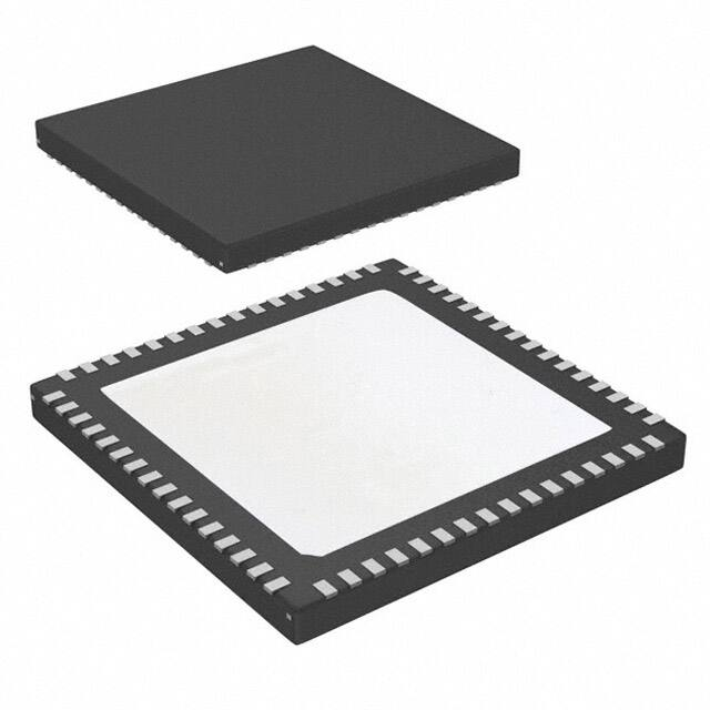
Package: 64-Pin WQFN (9 mm × 9 mm × 0.8 mm)
System Application Diagram
Backplane
•
•
•
•
•
•
•
•
•
•
10G, 40G, and 100G OTN Line Cards
SONET/SDH OC-48/STM-16 and OC-192/STM64 Line Cards
GbE/10GbE, 1/2/4/8/10GFC Line Cards
ITU G.709 and Custom FEC Line Cards
Synchronous Ethernet
Optical Modules
DSLAM/MSANs
Test and Measurement
Broadcast Video
Wireless Basestations
Data Converter Clocking
Microwave ODU and IDUs for Wireless Backhaul
3 Description
The LMK04906 is the industry's highest performance
clock jitter attenuator with superior clock jitter
cleaning, generation, and distribution with advanced
features to meet high performance timing application
needs.
The LMK04906 accepts 3 clock inputs ranging from 1
kHz to 500 MHz and generates 6 unique clock output
frequencies ranging from 284 kHz to 2.6 GHz. The
LMK04906 can also buffer a crystal or VCXO to
generate a 7th unique clock frequency.
The device provides virtually all frequency translation
combinations required for SONET, Ethernet, Fibre
Channel and multi-mode Wireless Base Stations.
The LMK04906 input clock frequency and clock
multiplication ratio are programmable through a SPI
interface.
Device Information(1)
PART NUMBER
LMK04906
VCO FREQUENCY
REFERENCE
INPUTS
2370 to 2600 MHz
3
(1) For all available packages, see the orderable addendum at
the end of the data sheet.
Simplified LMK04906 Block Diagram
Crystal or
VCXO
Hitless Switching, Jitter
Cleaning, Frequency
Multiplication, and
Programmable Clock
Distribution
LMK04906
156.25 MHz
LVPECL
10 GbE
PHY
10 GbE
PHY
100 MHz
LVDS
33.33 MHz
LVCMOS
FPGA
NPU
LMX2541
OSCout0
0XOWLSOH ³FOHDQ´
clocks at different
frequencies
PLL+VCO
LMK04906
CLKin0
Recovered
³GLUW\´ FORFNV
or clean clocks
SONET
CLKout2
CLKout3
CLKin2
Backup
Reference
Clock
SONET
CLKout1
Precision Clock
Conditioner
622.08,
155.52, 77.76,
19.44 MHz
Copyright © 2016, Texas Instruments Incorporated
Serializer/
Deserializer
CLKout0
LMK04906
CLKin1
ADC
CLKout4
FPGA
DAC
CPLD
Copyright © 2016, Texas Instruments Incorporated
1
An IMPORTANT NOTICE at the end of this data sheet addresses availability, warranty, changes, use in safety-critical applications,
intellectual property matters and other important disclaimers. PRODUCTION DATA.
�LMK04906
SNAS589F – JUNE 2012 – REVISED AUGUST 2017
www.ti.com
Table of Contents
1
2
3
4
5
6
Features ..................................................................
Applications ...........................................................
Description .............................................................
Revision History.....................................................
Pin Configuration and Functions .........................
Specifications.........................................................
6.1
6.2
6.3
6.4
6.5
6.6
6.7
7
1
1
1
2
3
5
Absolute Maximum Ratings ..................................... 5
ESD Ratings.............................................................. 5
Recommended Operating Conditions ...................... 5
Thermal Information .................................................. 5
Electrical Characteristics........................................... 6
Timing Requirements .............................................. 12
Typical Characteristics ............................................ 13
Parameter Measurement Information ................ 14
7.1 Charge Pump Current Specification Definitions...... 14
7.2 Differential Voltage Measurement Terminology...... 15
8
Detailed Description ............................................ 17
8.1
8.2
8.3
8.4
8.5
Overview .................................................................
Functional Block Diagram .......................................
Feature Description.................................................
Device Functional Modes........................................
Programming...........................................................
17
21
21
42
45
8.6 Register Maps ......................................................... 48
9
Application and Implementation ........................ 85
9.1
9.2
9.3
9.4
Application Information............................................ 85
Typical Application ............................................... 101
System Examples ................................................. 108
Do's and Don'ts ..................................................... 111
10 Power Supply Recommendations ................... 112
10.1 Pin Connection Recommendations..................... 112
10.2 Current Consumption and Power Dissipation
Calculations............................................................ 113
11 Layout................................................................. 115
11.1 Layout Guidelines ............................................... 115
11.2 Layout Example .................................................. 117
12 Device and Documentation Support ............... 118
12.1 Device Support....................................................
12.2 Receiving Notification of Documentation
Updates..................................................................
12.3 Community Resource..........................................
12.4 Trademarks .........................................................
12.5 Electrostatic Discharge Caution ..........................
12.6 Glossary ..............................................................
118
118
118
118
118
118
13 Mechanical, Packaging, and Orderable
Information ......................................................... 118
4 Revision History
NOTE: Page numbers for previous revisions may differ from page numbers in the current version.
Changes from Revision E (August 2016) to Revision F
Page
•
Changed From: CLKout3_PD = 0 To: CLKout2_PD = 0 in Table 7..................................................................................... 37
•
Changed From: CLKout3_PD = 0 To: CLKout2_PD = 0 in Table 9..................................................................................... 40
Changes from Revision D (May 2013) to Revision E
Page
•
Changed 750 to 500 ............................................................................................................................................................... 1
•
Changed 2.26 MHz to 284 kHz .............................................................................................................................................. 1
•
Added ESD Ratings table, Feature Description section, Device Functional Modes, Application and Implementation
section, Power Supply Recommendations section, Layout section, Device and Documentation Support section, and
Mechanical, Packaging, and Orderable Information section ................................................................................................. 1
•
Changed Clock Switch Event With Holdover section. .......................................................................................................... 26
•
Deleted Clock Switch Event without Holdover section. ........................................................................................................ 26
•
Changed 5 cycles to 5.5 cycles............................................................................................................................................ 38
•
Changed 5 cycles to 5.5 cycles............................................................................................................................................ 41
•
Added (Auto modes only). .................................................................................................................................................... 70
•
Changed equation ................................................................................................................................................................ 94
Changes from Revision C (May 2013) to Revision D
•
2
Page
Changed layout of National Semiconductor Data Sheet to TI format. ............................................................................... 115
Submit Documentation Feedback
Copyright © 2012–2017, Texas Instruments Incorporated
Product Folder Links: LMK04906
�LMK04906
www.ti.com
SNAS589F – JUNE 2012 – REVISED AUGUST 2017
5 Pin Configuration and Functions
NC
Status_CLKin1
Status_CLKin0
NC
NC
CLKout5*
CLKout5
Vcc12
NC
NC
CLKout4*
CLKout4
Vcc11
NC
CLKout3*
CLKout3
NKD Package
64-Pin WQFN With Exposed Pad
Top View
64
63
62
61
60
59
58
57
56
55
54
53
52
51
50
49
Vcc13
1
48
Vcc10
NC
2
47
NC
CLKout0*
3
46
DATAuWire
CLKout0
4
45
CLKuWire
NC
5
44
LEuWire
SYNC/
Status_CLKin2
6
43
Vcc9
NC
7
42
CPout2
NC
8
41
Vcc8
NC
9
40
OSCout0*
Vcc1
10
39
OSCout0
LDObyp1
11
38
Vcc7
LDObyp2
12
37
OSCin*
CLKout1
13
36
OSCin
CLKout1*
14
35
Vcc6
NC
15
34
CPout1
Vcc2
16
33
Status_LD
NC
27
28
29
30
31
32
CLKin2*
CLKout2
26
CLKin2
CLKout2*
25
Vcc5
NC
24
CLKin0*
NC
23
CLKin0
22
Status_Holdover
21
FBCLKin*/Fin*/CLKin1*
20
FBCLKin/Fin/CLKin1
19
GND
18
Vcc4
17
Vcc3
DAP
Pin Functions
PIN
I/O
TYPE
1
—
PWR
2, 5, 7, 8, 9, 15,
17, 19
22, 47, 51, 55,
56, 60,
61, 64
—
No Connect
NAME
NO.
Vcc13
NC
CLKout0*, CLKout0
DESCRIPTION (1)
Power Supply for CLKou0
These pins must be left floating.
3, 4
O
Programmable Clock output 0.
SYNC /
Status_CLKin2
6
I/O
Programmable CLKout Synchronization input or CLKin2 Status output.
Vcc1
10
—
PWR
Power supply for VCO LDO.
LDObyp1
11
—
ANLG
LDO Bypass, bypassed to ground with 10 µF capacitor.
(1)
See Application and Implementation section for recommended connections.
Submit Documentation Feedback
Copyright © 2012–2017, Texas Instruments Incorporated
Product Folder Links: LMK04906
3
�LMK04906
SNAS589F – JUNE 2012 – REVISED AUGUST 2017
www.ti.com
Pin Functions (continued)
PIN
NAME
NO.
LDObyp2
CLKout1, CLKout1*
Vcc2
Vcc3
I/O
12
—
13, 14
O
16
—
DESCRIPTION (1)
TYPE
ANLG
LDO Bypass, bypassed to ground with a 0.1 µF capacitor.
Programmable Clock output 1.
PWR
Power supply for CLKout1.
PWR
Power supply for CLKout2
18
—
20, 21
O
GND
23
—
PWR
Ground
Vcc4
24
—
PWR
Power supply for digital.
CLKout2*, CLKout2
Programmable Clock output 2
CLKin1, CLKin1*
FBCLKin, FBCLKin*
Reference Clock Input Port 1 for PLL1. AC or DC Coupled.
25, 26
I
ANLG
Fin/Fin*
Feedback input for external clock feedback input (0-delay mode).
AC or DC Coupled.
External VCO input (External VCO mode). AC or DC Coupled.
Programmable status pin, default readback output. Programmable
Programmable to holdover mode indicator. Other options available by
programming.
Status_Holdover
27
I/O
CLKin0, CLKin0*
28, 29
I
ANLG
Reference Clock Input Port 0 for PLL1.
AC or DC Coupled.
30
—
PWR
Power supply for clock inputs.
31, 32
I
ANLG
Reference Clock Input Port 2 for PLL1,
AC or DC Coupled.
Status_LD
33
I/O
Programmable
CPout1
34
O
ANLG
Charge pump 1 output.
Vcc6
35
—
PWR
Power supply for PLL1, charge pump 1.
36, 37
I
ANLG
Feedback to PLL1, Reference input to PLL2.
AC Coupled.
PWR
Power supply for OSCin port.
Vcc5
CLKin2, CLKin2*
OSCin, OSCin*
Vcc7
Programmable status pin, default lock detect for PLL1 and PLL2.
Other options available by programming.
38
—
39, 40
O
Vcc8
41
—
PWR
Power supply for PLL2, charge pump 2.
CPout2
42
O
ANLG
Charge pump 2 output.
Vcc9
43
—
PWR
Power supply for PLL2.
LEuWire
44
I
CMOS
MICROWIRE Latch Enable Input.
CLKuWire
45
I
CMOS
MICROWIRE Clock Input.
DATAuWire
46
I
CMOS
MICROWIRE Data Input.
Vcc10
48
—
PWR
OSCout0, OSCout0*
CLKout3, CLKout3*
Vcc11
CLKout4, CLKout4*
Vcc12
49, 50
O
52
—
53, 54
O
Programmable Buffered output 0 of OSCin port.
Power supply for CLKout3.
Programmable Clock output 3.
PWR
Power supply for CLKout4.
Programmable Clock output 4.
57
—
58, 59
O
Programmable Clock output 5.
Status_CLKin0
62
I/O
Programmable status pin. Default is input for pin control of PLL1
Programmable reference clock selection. CLKin0 LOS status and other options
available by programming.
Status_CLKin1
63
I/O
Programmable status pin. Default is input for pin control of PLL1
Programmable reference clock selection. CLKin1 LOS status and other options
available by programming.
DAP
—
CLKout5, CLKout5*
DAP
4
PWR
GND
Power supply for CLKout5.
DIE ATTACH PAD, connect to GND.
Submit Documentation Feedback
Copyright © 2012–2017, Texas Instruments Incorporated
Product Folder Links: LMK04906
�LMK04906
www.ti.com
SNAS589F – JUNE 2012 – REVISED AUGUST 2017
6 Specifications
6.1 Absolute Maximum Ratings
over operating free-air temperature range (unless otherwise noted) (1) (2)
(3)
VCC
Supply voltage
VIN
Input voltage
IIN
Differential input current (CLKinX/X*,
OSCin/OSCin*, FBCLKin/FBCLKin*, Fin/Fin*)
MSL
Moisture sensitivity level
TJ
Junction temperature
Tstg
Storage temperature
(1)
(2)
(3)
MIN
MAX
UNIT
–0.3
3.6
V
–0.3
(VCC + 0.3)
V
±5
mA
3
–65
150
°C
150
°C
Stresses beyond those listed under Absolute Maximum Ratings may cause permanent damage to the device. These are stress ratings
only, which do not imply functional operation of the device at these or any other conditions beyond those indicated under Recommended
Operating Conditions. Exposure to absolute-maximum-rated conditions for extended periods may affect device reliability.
If Military/Aerospace specified devices are required, please contact the Texas Instruments Sales Office/Distributors for availability and
specifications.
Never to exceed 3.6 V.
6.2 ESD Ratings
VALUE
V(ESD)
(1)
(2)
Electrostatic discharge
Human-body model (HBM), per ANSI/ESDA/JEDEC JS-001 (1)
±2000
Charged-device model (CDM), per JEDEC specification JESD22C101 (2)
±750
Machine model (MM)
±150
UNIT
V
JEDEC document JEP155 states that 500-V HBM allows safe manufacturing with a standard ESD control process.
JEDEC document JEP157 states that 250-V CDM allows safe manufacturing with a standard ESD control process.
6.3 Recommended Operating Conditions
TJ
Junction temperature
TA
Ambient temperature
VCC
Supply voltage
VCC = 3.3 V
MIN
NOM
–40
25
3.15
3.3
MAX
UNIT
125
°C
85
°C
3.45
V
6.4 Thermal Information
LMK04906
THERMAL METRIC (1)
NKD (WQFN)
UNIT
64 PINS
RθJA
Junction-to-ambient thermal resistance
25.2
°C/W
RθJC(top)
Junction-to-case (top) thermal resistance
6.9
°C/W
RθJB
Junction-to-board thermal resistance
ψJT
Junction-to-top characterization parameter
ψJB
RθJC(bot)
(1)
4
°C/W
0.1
°C/W
Junction-to-board characterization parameter
4
°C/W
Junction-to-case (bottom) thermal resistance
0.8
°C/W
For more information about traditional and new thermal metrics, see the Semiconductor and IC Package Thermal Metrics application
report.
Submit Documentation Feedback
Copyright © 2012–2017, Texas Instruments Incorporated
Product Folder Links: LMK04906
5
�LMK04906
SNAS589F – JUNE 2012 – REVISED AUGUST 2017
www.ti.com
6.5 Electrical Characteristics
(3.15 V ≤ VCC ≤ 3.45 V, -40 °C ≤ TA ≤ 85 °C. Typical values represent most likely parametric norms at VCC = 3.3 V, TA = 25
°C, at the Recommended Operating Conditions at the time of product characterization and are not ensured.)
PARAMETER
TEST CONDITIONS
MIN
TYP
MAX
UNIT
1
3
mA
410
470
mA
500
MHz
CURRENT CONSUMPTION
ICC_PD
Power Down Supply Current
ICC_CLKS
Supply Current with all clocks enabled
(1)
All clock delays disabled,
CLKoutX_DIV = 1045,
CLKoutX_TYPE = 1 (LVDS),
PLL1 and PLL2 locked.
CLKin0/0*, CLKin1/1*, and CLKin2/2* INPUT CLOCK SPECIFICATIONS
Clock Input Frequency
fCLKin
0.001
(2)
SLEWCLKin
VIDCLKin
VSSCLKin
VIDCLKin
VSSCLKin
Clock Input Slew Rate
(3)
Clock Input
Differential Input Voltage
0.15
AC coupled
CLKinX_BUF_TYPE = 0 (Bipolar)
0.25
AC coupled
CLKinX_BUF_TYPE = 1 (MOS)
Figure 4
(3)
VCLKin0-offset
DC offset voltage between
CLKin0/CLKin0*
CLKin0* - CLKin0
VCLKin1-offset
DC offset voltage between
CLKin1/CLKin1*
CLKin1* - CLKin1
VCLKin2-offset
DC offset voltage between
CLKin2/CLKin2*
CLKin2* - CLKin2
VCLKinX-offset
DC offset voltage between
CLKinX/CLKinX*
CLKinX* - CLKinX
VCLKin- VIH
High input voltage
VCLKin- VIL
Low input voltage
0.5
V/ns
1.55
|V|
0.5
3.1
Vpp
0.25
1.55
|V|
0.5
3.1
Vpp
AC coupled to CLKinX; CLKinX* AC
coupled to Ground
CLKinX_BUF_TYPE = 0 (Bipolar)
0.25
2.4
Vpp
AC coupled to CLKinX; CLKinX* AC
coupled to Ground
CLKinX_BUF_TYPE = 1 (MOS)
0.25
2.4
Vpp
(4)
Clock Input
Single-ended Input Voltage
VCLKin
20% to 80%
Each pin AC coupled
CLKin0_BUF_TYPE = 0 (Bipolar)
Each pin AC coupled
CLKinX_BUF_TYPE = 1 (MOS)
DC coupled to CLKinX; CLKinX* AC
coupled to Ground
CLKinX_BUF_TYPE = 1 (MOS)
20
mV
0
mV
20
mV
55
mV
2
VCC
V
0
0.4
V
AC coupled
(CLKinX_BUF_TYPE = 0)
MODE = 2 or 8; FEEDBACK_MUX = 6
0.001
1000
MHz
AC coupled
(CLKinX_BUF_TYPE = 0)
MODE = 3 or 11
0.001
3100
MHz
AC coupled;
(CLKinX_BUF_TYPE = 0)
0.25
2
Vpp
AC coupled; 20% to 80%;
(CLKinX_BUF_TYPE = 0)
0.15
FBCLKin/FBCLKin* and Fin/Fin* INPUT SPECIFICATIONS
Clock Input Frequency
fFBCLKin
(3)
Clock Input Frequency
fFin
(3)
VFBCLKin/Fin
SLEWFBCLKin/Fin
(1)
(2)
(3)
(4)
6
Single Ended
Clock Input Voltage
(3)
Slew Rate on CLKin
(3)
0.5
V/ns
Load conditions for output clocks: LVDS: 100 Ω differential. See Current Consumption and Power Dissipation Calculations for ICC for
specific part configuration and how to calculate ICC for a specific design.
CLKin0, CLKin1, and CLKin2 maximum is specified by characterization, production tested at 200 MHz.
Specified by characterization.
See Differential Voltage Measurement Terminology for definition of VID and VOD voltages.
Submit Documentation Feedback
Copyright © 2012–2017, Texas Instruments Incorporated
Product Folder Links: LMK04906
�LMK04906
www.ti.com
SNAS589F – JUNE 2012 – REVISED AUGUST 2017
Electrical Characteristics (continued)
(3.15 V ≤ VCC ≤ 3.45 V, -40 °C ≤ TA ≤ 85 °C. Typical values represent most likely parametric norms at VCC = 3.3 V, TA = 25
°C, at the Recommended Operating Conditions at the time of product characterization and are not ensured.)
PARAMETER
TEST CONDITIONS
MIN
TYP
MAX
UNIT
40
MHz
PLL1 SPECIFICATIONS
fPD1
PLL1 Phase Detector Frequency
ICPout1SOURCE
PLL1 Charge
Pump Source Current
(5)
VCPout1 = VCC/2, PLL1_CP_GAIN = 0
100
VCPout1 = VCC/2, PLL1_CP_GAIN = 1
200
VCPout1 = VCC/2, PLL1_CP_GAIN = 2
400
VCPout1 = VCC/2, PLL1_CP_GAIN = 3
1600
VCPout1=VCC/2, PLL1_CP_GAIN = 0
–100
VCPout1=VCC/2, PLL1_CP_GAIN = 1
–200
VCPout1=VCC/2, PLL1_CP_GAIN = 2
–400
VCPout1=VCC/2, PLL1_CP_GAIN = 3
–1600
ICPout1SINK
PLL1 Charge
Pump Sink Current
ICPout1%MIS
Charge Pump
Sink / Source Mismatch
VCPout1 = VCC/2, T = 25 °C
3%
ICPout1VTUNE
Magnitude of Charge Pump Current
Variation vs. Charge Pump Voltage
0.5 V < VCPout1 < VCC - 0.5 V
TA = 25 °C
4%
ICPout1%TEMP
Charge Pump Current vs. Temperature
Variation
ICPout1 TRI
Charge Pump TRI-STATELeakage
Current
PN10kHz
PLL 1/f Noise at 10-kHz offset.
Normalized to 1-GHz Output
Frequency
PN1Hz
Normalized Phase Noise Contribution
(5)
µA
µA
10
4%
0.5 V < VCPout < VCC - 0.5 V
5
PLL1_CP_GAIN = 400 µA
–117
PLL1_CP_GAIN = 1600 µA
–118
PLL1_CP_GAIN = 400 µA
dBc/Hz
–221.5
PLL1_CP_GAIN = 1600 µA
nA
dBc/Hz
–223
PLL2 REFERENCE INPUT (OSCin) SPECIFICATIONS
fOSCin
SLEWOSCin
PLL2 Reference Input
500
(6)
PLL2 Reference Clock minimum slew
rate on OSCin (3)
0.15
(3)
AC coupled; Single-ended (Unused pin
AC coupled to GND)
Differential voltage swing
Figure 4
AC coupled
VOSCin-offset
DC offset voltage between
OSCin/OSCin*
OSCinX* - OSCinX
Each pin AC coupled
fdoubler_max
Doubler input frequency
VOSCin
VIDOSCin
VSSOSCin
Input Voltage for OSCin or OSCin*
20% to 80%
0.5
V/ns
0.2
2.4
0.2
1.55
|V|
0.4
3.1
Vpp
20
EN_PLL2_REF_2X = 1;
OSCin Duty Cycle 40% to 60%
(3)
MHz
Vpp
mV
155
MHz
20.5
MHz
CRYSTAL OSCILLATOR MODE SPECIFICATIONS
fXTAL
Crystal frequency range
RESR < 40 Ω
(3)
Vectron VXB1 crystal, 20.48 MHz,
RESR < 40 Ω
XTAL_LVL = 0
(7)
PXTAL
Crystal power dissipation
CIN
Input capacitance of LMK04906 OSCin
port
(5)
(6)
(7)
–40 to +85 °C
6
100
µW
6
pF
This parameter is programmable
FOSCin maximum frequency specified by characterization. Production tested at 200 MHz.
See Optional Crystal Oscillator Implementation (OSCin/OSCin*)
Submit Documentation Feedback
Copyright © 2012–2017, Texas Instruments Incorporated
Product Folder Links: LMK04906
7
�LMK04906
SNAS589F – JUNE 2012 – REVISED AUGUST 2017
www.ti.com
Electrical Characteristics (continued)
(3.15 V ≤ VCC ≤ 3.45 V, -40 °C ≤ TA ≤ 85 °C. Typical values represent most likely parametric norms at VCC = 3.3 V, TA = 25
°C, at the Recommended Operating Conditions at the time of product characterization and are not ensured.)
PARAMETER
TEST CONDITIONS
MIN
TYP
MAX
UNIT
155
MHz
PLL2 PHASE DETECTOR AND CHARGE PUMP SPECIFICATIONS
fPD2
Phase detector frequency
ICPoutSOURCE
PLL2 charge pump source current
(5)
(5)
VCPout2=VCC/2, PLL2_CP_GAIN = 0
100
VCPout2=VCC/2, PLL2_CP_GAIN = 1
400
VCPout2=VCC/2, PLL2_CP_GAIN = 2
1600
VCPout2=VCC/2, PLL2_CP_GAIN = 3
3200
VCPout2=VCC/2, PLL2_CP_GAIN = 0
–100
VCPout2=VCC/2, PLL2_CP_GAIN = 1
–400
VCPout2=VCC/2, PLL2_CP_GAIN = 2
–1600
VCPout2=VCC/2, PLL2_CP_GAIN = 3
–3200
ICPoutSINK
PLL2 charge pump sink current
ICPout2%MIS
Charge pump sink/source mismatch
VCPout2=VCC/2, TA = 25 °C
3%
ICPout2VTUNE
Magnitude of charge pump current vs
charge pump voltage variation
0.5 V < VCPout2 < VCC - 0.5 V
TA = 25 °C
4%
ICPout2%TEMP
Charge pump current vs temperature
variation
ICPout2TRI
Charge pump leakage
0.5 V < VCPout2 < VCC – 0.5 V
PLL2_CP_GAIN = 400 µA
–118
PN10kHz
PLL 1/f noise at 10-kHz offset
(8)
. Normalized to
1-GHz output frequency
PLL2_CP_GAIN = 3200 µA
–121
PN1Hz
Normalized phase noise contribution
µA
µA
10%
4%
(9)
10
PLL2_CP_GAIN = 400 µA
dBc/Hz
–222.5
PLL2_CP_GAIN = 3200 µA
nA
dBc/Hz
–227
INTERNAL VCO SPECIFICATIONS
fVCO
VCO tuning range
KVCO
Fine tuning sensitivity
(The range displayed in the typical
column indicates the lower sensitivity is
typical at the lower end of the tuning
LMK04906
range, and the higher tuning sensitivity
is typical at the higher end of the tuning
range).
|ΔTCL|
Allowable temperature drift for
continuous lock
(10) (3)
LMK04906
2370
2600
16 to 21
After programming R30 for lock, no
changes to output configuration are
permitted to guarantee continuous lock
MHz
MHz/V
125
°C
(8)
A specification in modeling PLL in-band phase noise is the 1/f flicker noise, LPLL_flicker(f), which is dominant close to the carrier. Flicker
noise has a 10 dB/decade slope. PN10kHz is normalized to a 10 kHz offset and a 1 GHz carrier frequency. PN10kHz = LPLL_flicker(10
kHz) - 20log(Fout / 1 GHz), where LPLL_flicker(f) is the single side band phase noise of only the flicker noise's contribution to total noise,
L(f). To measure LPLL_flicker(f) it is important to be on the 10 dB/decade slope close to the carrier. A high compare frequency and a clean
crystal are important to isolating this noise source from the total phase noise, L(f). LPLL_flicker(f) can be masked by the reference
oscillator performance if a low power or noisy source is used. The total PLL in-band phase noise performance is the sum of LPLL_flicker(f)
and LPLL_flat(f).
(9) A specification modeling PLL in-band phase noise. The normalized phase noise contribution of the PLL, LPLL_flat(f), is defined as:
PN1HZ=LPLL_flat(f) - 20log(N) - 10log(fPDX). LPLL_flat(f) is the single side band phase noise measured at an offset frequency, f, in a 1 Hz
bandwidth and fPDX is the phase detector frequency of the synthesizer. LPLL_flat(f) contributes to the total noise, L(f).
(10) Maximum Allowable Temperature Drift for Continuous Lock is how far the temperature can drift in either direction from the value it was
at the time that the R30 register was last programmed, and still have the part stay in lock. The action of programming the R30 register,
even to the same value, activates a frequency calibration routine. This implies the part will work over the entire frequency range, but if
the temperature drifts more than the maximum allowable drift for continuous lock, then it will be necessary to reload the R30 register to
ensure it stays in lock. Regardless of what temperature the part was initially programmed at, the temperature can never drift outside the
frequency range of -40 °C to 85 °C without violating specifications.
8
Submit Documentation Feedback
Copyright © 2012–2017, Texas Instruments Incorporated
Product Folder Links: LMK04906
�LMK04906
www.ti.com
SNAS589F – JUNE 2012 – REVISED AUGUST 2017
Electrical Characteristics (continued)
(3.15 V ≤ VCC ≤ 3.45 V, -40 °C ≤ TA ≤ 85 °C. Typical values represent most likely parametric norms at VCC = 3.3 V, TA = 25
°C, at the Recommended Operating Conditions at the time of product characterization and are not ensured.)
PARAMETER
TEST CONDITIONS
CLKout CLOSED LOOP JITTER SPECIFICATIONS USING A COMMERCIAL QUALITY VCXO
L(f)CLKout
LMK04906
fCLKout = 245.76 MHz
SSB phase noise
Measured at clock outputs
Value is average for all output types
MIN
TYP
MAX
UNIT
(11)
Offset = 1 kHz
–122.5
Offset = 10 kHz
–132.9
Offset = 100 kHz
–135.2
Offset = 800 kHz
–143.9
Offset = 10 MHz; LVDS
dBc/Hz
–156
(12)
JCLKout
LVDS/LVPECL/
LVCMOS
LMK04906 (12)
fCLKout = 245.76 MHz
Integrated RMS jitter
Offset = 10 MHz; LVPECL 1600 mVpp
–157.5
Offset = 10 MHz; LVCMOS
–157.1
BW = 12 kHz to 20 MHz
115
BW = 100 Hz to 20 MHz
123
fs rms
CLKout CLOSED LOOP JITTER SPECIFICATIONS USING THE INTEGRATED LOW NOISE CRYSTAL OSCILLATOR CIRCUIT
LMK04906
fCLKout = 245.76 MHz
Integrated RMS jitter
BW = 12 kHz to 20 MHz
XTAL_LVL = 3
192
BW = 100 Hz to 20 MHz
XTAL_LVL = 3
450
(13)
DEFAULT POWER ON RESET CLOCK OUTPUT FREQUENCY
fCLKout-startup
Default output clock frequency at
device power on
CLKout4, LVDS, LMK04906
(14)
90
98
110
MHz
CLOCK SKEW AND DELAY
LVDS-to-LVDS, T = 25 °C,
FCLK = 800 MHz, RL= 100 Ω
AC coupled
30
LVPECL-to-LVPECL,
T = 25 °C,
FCLK = 800 MHz, RL= 100 Ω
emitter resistors =
240 Ω to GND
AC coupled
30
Maximum skew between any two
LVCMOS outputs, same CLKout or
different CLKout (15) (3)
RL = 50 Ω, CL = 5 pF,
T = 25 °C, FCLK = 100 MHz.
100
LVDS or LVPECL to LVCMOS
Same device, T = 25 °C,
250 MHz
750
Maximum CLKoutX to CLKoutY
(15) (3)
|TSKEW|
MixedTSKEW
td0-DELAY
CLKin to CLKoutX delay
(15)
(15)
MODE = 2
PLL1_R_DLY = 0; PLL1_N_DLY = 0
1850
MODE = 2
PLL1_R_DLY = 0; PLL1_N_DLY = 0;
VCO Frequency = 2949.12 MHz
Analog delay select = 0;
Feedback clock digital delay = 11;
Feedback clock half step = 1;
Output clock digital delay = 5;
Output clock half step = 0;
0
ps
ps
ps
(11) VCXO used is a 122.88 MHz Crystek CVHD-950-122.880.
(12) fVCO = 2457.6 MHz, PLL1 parameters: EN_PLL2_REF_2X = 1, PLL2_R = 2, FPD1 = 1.024 MHz, ICP1 = 100 μA, loop bandwidth = 10 Hz.
A 122.88 MHz Crystek CVHD-950–122.880. PLL2 parameters: PLL2_R = 1, FPD2 = 122.88 MHz, ICP2 = 3200 μA, C1 = 47 pF, C2 = 3.9
nF, R2 = 620 Ω, PLL2_C3_LF = 0, PLL2_R3_LF = 0, PLL2_C4_LF = 0, PLL2_R4_LF = 0, CLKoutX_DIV = 10, and
CLKoutX_ADLY_SEL = 0.
(13) Crystal used is a 20.48 MHz Vectron VXB1-1150-20M480 and Skyworks varactor diode, SMV-1249-074LF.
(14) CLKout3 and OSCout0 also oscillate at start-up at the frequency of the VCXO attached to OSCin port.
(15) Equal loading and identical clock output configuration on each clock output is required for specification to be valid. Specification not valid
for delay mode.
Submit Documentation Feedback
Copyright © 2012–2017, Texas Instruments Incorporated
Product Folder Links: LMK04906
9
�LMK04906
SNAS589F – JUNE 2012 – REVISED AUGUST 2017
www.ti.com
Electrical Characteristics (continued)
(3.15 V ≤ VCC ≤ 3.45 V, -40 °C ≤ TA ≤ 85 °C. Typical values represent most likely parametric norms at VCC = 3.3 V, TA = 25
°C, at the Recommended Operating Conditions at the time of product characterization and are not ensured.)
PARAMETER
TEST CONDITIONS
MIN
TYP
MAX
UNIT
LVDS CLOCK OUTPUTS (CLKoutX), CLKoutX_TYPE = 1
fCLKout
VOD
Maximum frequency
RL = 100 Ω
(3) (16)
VSS
Differential output voltage
Figure 5
ΔVOD
Change in Magnitude of VOD for
complementary output states
VOS
Output offset voltage
ΔVOS
Change in VOS for complementary
output states
1536
T = 25 °C, DC measurement
AC coupled to receiver input
R = 100 Ω differential termination
MHz
250
400
450
|mV|
500
800
900
mVpp
50
mV
–50
1.125
1.25
1.375
35
V
|mV|
Output rise time
20% to 80%, RL = 100 Ω
Output fall time
80% to 20%, RL = 100 Ω
ISA
ISB
Output short-circuit current: single
ended
Single-ended output shorted to GND, T
= 25 °C
–24
24
mA
ISAB
Output short-circuit current: differential
Complimentary outputs tied together
–12
12
mA
TR / TF
200
ps
LVPECL CLOCK OUTPUTS (CLKoutX)
fCLKout
Maximum frequency
20% to 80% output rise
TR / TF
1536
(3) (16)
80% to 20% output fall time
RL = 100 Ω, emitter resistors = 240 Ω
to GND
CLKoutX_TYPE = 4 or 5
(1600 or 2000 mVpp)
MHz
150
ps
VCC –
1.03
V
VCC –
1.41
V
700-mVpp LVPECL CLOCK OUTPUTS (CLKoutX), CLKoutX_TYPE = 2
VOH
Output high voltage
VOL
Output low voltage
VOD
Output voltage
Figure 5
VSS
T = 25 °C, DC measurement
Termination = 50 Ω to
VCC - 1.4 V
305
380
440
|mV|
610
760
880
mVpp
1200-mVpp LVPECL CLOCK OUTPUTS (CLKoutX), CLKoutX_TYPE = 3
VOH
Output high voltage
VOL
Output low voltage
VOD
Output voltage
Figure 5
VSS
T = 25 °C, DC measurement
Termination = 50 Ω to
VCC – 1.7 V
VCC –
1.07
V
VCC –
1.69
V
545
625
705
|mV|
1090
1250
1410
mVpp
1600-mVpp LVPECL CLOCK OUTPUTS (CLKoutX), CLKoutX_TYPE = 4
VOH
Output high voltage
VOL
Output low voltage
VOD
Output voltage
Figure 5
VSS
T = 25 °C, DC Measurement
Termination = 50 Ω to
VCC – 2 V
VCC –
1.10
V
VCC –
1.97
V
660
870
965
|mV|
1320
1740
1930
mVpp
(16) See Typical Characteristics for output operation performance at higher frequencies than the minimum maximum output frequency.
10
Submit Documentation Feedback
Copyright © 2012–2017, Texas Instruments Incorporated
Product Folder Links: LMK04906
�LMK04906
www.ti.com
SNAS589F – JUNE 2012 – REVISED AUGUST 2017
Electrical Characteristics (continued)
(3.15 V ≤ VCC ≤ 3.45 V, -40 °C ≤ TA ≤ 85 °C. Typical values represent most likely parametric norms at VCC = 3.3 V, TA = 25
°C, at the Recommended Operating Conditions at the time of product characterization and are not ensured.)
PARAMETER
TEST CONDITIONS
MIN
TYP
MAX
UNIT
2000-mVpp LVPECL (2VPECL) CLOCK OUTPUTS (CLKoutX), CLKoutX_TYPE = 5
VOH
Output high voltage
VOL
Output low voltage
VOD
Output voltage
Figure 5
VSS
T = 25 °C, DC Measurement
Termination = 50 Ω to
VCC – 2.3 V
VCC –
1.13
V
VCC –
2.20
V
800
1070
1200
|mV|
1600
2140
2400
mVpp
LVCMOS CLOCK OUTPUTS (CLKoutX)
fCLKout
Maximum frequency
(3) (16)
5-pF Load
VOH
Output high voltage
1-mA Load
VOL
Output low voltage
1-mA Load
IOH
Output high current (source)
VCC = 3.3 V, VO = 1.65 V
28
mA
IOL
Output low current (sink)
VCC = 3.3 V, VO = 1.65 V
28
mA
Output duty cycle
(3)
VCC/2 to VCC/2, FCLK = 100 MHz, T =
25 °C
TR
Output rise time
20% to 80%, RL = 50 Ω,
CL = 5 pF
400
ps
TF
Output fall time
80% to 20%, RL = 50 Ω,
CL = 5 pF
400
ps
DUTYCLK
250
MHz
VCC –
0.1
V
0.1
45%
50%
V
55%
DIGITAL OUTPUTS (Status_CLKinX, Status_LD, Status_Holdover, SYNC)
VOH
High-level output voltage
IOH = -500 µA
VOL
Low-level output voltage
IOL = 500 µA
VCC –
0.4
V
0.4
V
VCC
V
0.4
V
DIGITAL INPUTS (Status_CLKinX, SYNC)
VIH
High-level input voltage
VIL
Low-level input voltage
IIH
IIL
1.6
High-level input current
VIH = VCC
Low-level input current
VIL = 0 V
Status_CLKinX_TYPE = 0
(High Impedance)
–5
5
Status_CLKinX_TYPE = 1
(Pull-up)
–5
5
Status_CLKinX_TYPE = 2
(Pull-down)
10
80
Status_CLKinX_TYPE = 0
(High Impedance)
–5
5
Status_CLKinX_TYPE = 1
(Pull-up)
–40
–5
Status_CLKinX_TYPE = 2
(Pulldown)
–5
5
1.6
VCC
V
0.4
V
5
25
µA
–5
5
µA
µA
µA
DIGITAL INPUTS (CLKuWire, DATAuWire, LEuWire)
VIH
High-level input voltage
VIL
Low-level input voltage
IIH
High-level input current
VIH = VCC
IIL
Low-level input current
VIL = 0
Submit Documentation Feedback
Copyright © 2012–2017, Texas Instruments Incorporated
Product Folder Links: LMK04906
11
�LMK04906
SNAS589F – JUNE 2012 – REVISED AUGUST 2017
www.ti.com
6.6 Timing Requirements
MIN
NOM
MAX
UNIT
TECS
LE to Clock Set Up Time
See Figure 6
25
ns
TDCS
Data to Clock Set Up Time
See Figure 6
25
ns
TCDH
Clock to Data Hold Time
See Figure 6
8
ns
TCWH
Clock Pulse Width High
See Figure 6
25
ns
TCWL
Clock Pulse Width Low
See Figure 6
25
ns
TCES
Clock to LE Set Up Time
See Figure 6
25
ns
TEWH
LE Pulse Width
See Figure 6
25
ns
TCR
Falling Clock to Readback Time
See Figure 9
25
ns
12
Submit Documentation Feedback
Copyright © 2012–2017, Texas Instruments Incorporated
Product Folder Links: LMK04906
�LMK04906
www.ti.com
SNAS589F – JUNE 2012 – REVISED AUGUST 2017
6.7 Typical Characteristics
1200
500
2000 mVpp
1600 mVpp
1200 mVpp
700 mVpp
450
1000
400
VOD(mV)
VOD(mV)
350
300
250
200
800
600
400
150
100
200
50
0
0
0
500
1000 1500 2000 2500 3000
FREQUENCY (MHz)
0
Figure 1. LVDS VOD vs Frequency
500 1000 1500 2000 2500 3000
FREQUENCY (MHz)
Figure 2. LVPECL With 240-Ω Emitter Resistors VOD vs
Frequency
1200
VOD(mV)
1000
2000 mVpp
800
600
1600 mVpp
400
200
0
0
500 1000 1500 2000 2500 3000
FREQUENCY (MHz)
Figure 3. LVPECL With 120-Ω Emitter Resistors VOD vs Frequency
Submit Documentation Feedback
Copyright © 2012–2017, Texas Instruments Incorporated
Product Folder Links: LMK04906
13
�LMK04906
SNAS589F – JUNE 2012 – REVISED AUGUST 2017
www.ti.com
7 Parameter Measurement Information
7.1 Charge Pump Current Specification Definitions
I1 = Charge Pump Sink Current at VCPout = VCC - ΔV
I2 = Charge Pump Sink Current at VCPout = VCC/2
I3 = Charge Pump Sink Current at VCPout = ΔV
I4 = Charge Pump Source Current at VCPout = VCC - ΔV
I5 = Charge Pump Source Current at VCPout = VCC/2
I6 = Charge Pump Source Current at VCPout = ΔV
ΔV = Voltage offset from the positive and negative supply rails. Defined to be 0.5 V for this device.
7.1.1 Charge Pump Output Current Magnitude Variation Vs. Charge Pump Output Voltage
ICPout Vs VCPout =
=
I1 - I3
´ 100%
I1 + I3
I4 - I6
I4 + I6
´ 100%
7.1.2 Charge Pump Sink Current Vs. Charge Pump Output Source Current Mismatch
ICPout Sink Vs ICPout Source =
14
I2 - I5
I2 + I5
Submit Documentation Feedback
´ 100%
Copyright © 2012–2017, Texas Instruments Incorporated
Product Folder Links: LMK04906
�LMK04906
www.ti.com
SNAS589F – JUNE 2012 – REVISED AUGUST 2017
Charge Pump Current Specification Definitions (continued)
7.1.3 Charge Pump Output Current Magnitude Variation vs Temperature
I2
ICPout Vs TA =
TA - I2
I2
I5
=
´ 100%
TA = 25°C
TA - I5
I5
TA = 25°C
TA = 25°C
´ 100%
TA = 25°C
7.2 Differential Voltage Measurement Terminology
The differential voltage of a differential signal can be described by two different definitions causing confusion
when reading datasheets or communicating with other engineers. This section will address the measurement and
description of a differential signal so that the reader will be able to understand and discern between the two
different definitions when used.
The first definition used to describe a differential signal is the absolute value of the voltage potential between the
inverting and non-inverting signal. The symbol for this first measurement is typically VID or VOD depending on if
an input or output voltage is being described.
The second definition used to describe a differential signal is to measure the potential of the non-inverting signal
with respect to the inverting signal. The symbol for this second measurement is VSS and is a calculated
parameter. Nowhere in the IC does this signal exist with respect to ground, it only exists in reference to its
differential pair. VSS can be measured directly by oscilloscopes with floating references, otherwise this value can
be calculated as twice the value of VOD as described in the first description.
Figure 4 illustrates the two different definitions side-by-side for inputs and Figure 5 illustrates the two different
definitions side-by-side for outputs. The VID and VOD definitions show VA and VB DC levels that the non-inverting
and inverting signals toggle between with respect to ground. VSS input and output definitions show that if the
inverting signal is considered the voltage potential reference, the non-inverting signal voltage potential is now
increasing and decreasing above and below the non-inverting reference. Thus the peak-to-peak voltage of the
differential signal can be measured.
VID and VOD are often defined as volts (V) and VSS is often defined as volts peak-to-peak (VPP).
VID Definition
VSS Definition for Input
Non-Inverting Clock
VA
2· VID
VID
VB
Inverting Clock
VID = | VA - VB |
VSS = 2· VID
GND
Figure 4. Two Different Definitions for Differential Input Signals
Submit Documentation Feedback
Copyright © 2012–2017, Texas Instruments Incorporated
Product Folder Links: LMK04906
15
�LMK04906
SNAS589F – JUNE 2012 – REVISED AUGUST 2017
www.ti.com
Differential Voltage Measurement Terminology (continued)
VOD Definition
VSS Definition for Output
Non-Inverting Clock
VA
2· VOD
VOD
VB
Inverting Clock
VOD = | VA - VB |
VSS = 2· VOD
GND
See the AN-912 Common Data Transmission Parameters and Their Definitions (SNLA036) application note for more
information.
Figure 5. Two Different Definitions for Differential Output Signals
16
Submit Documentation Feedback
Copyright © 2012–2017, Texas Instruments Incorporated
Product Folder Links: LMK04906
�LMK04906
www.ti.com
SNAS589F – JUNE 2012 – REVISED AUGUST 2017
8 Detailed Description
8.1 Overview
In default mode of operation, dual PLL mode with internal VCO, the Phase Frequency Detector in PLL1
compares the active CLKinX reference divided by CLKinX_PreR_DIV and PLL1 R divider with the external
VCXO or crystal attached to the PLL2 OSCin port divided by PLL1 N divider. The external loop filter for PLL1
should be narrow to provide an ultra clean reference clock from the external VCXO or crystal to the
OSCin/OSCin* pins for PLL2.
The Phase Frequency Detector in PLL2 compares the external VCXO or crystal attached to the OCSin port
divided by the PLL2 R divider with the output of the internal VCO divided by the PLL2 N divider and N2 prescaler and optionally the VCO divider. The bandwidth of the external loop filter for PLL2 should be designed to
be wide enough to take advantage of the low in-band phase noise of PLL2 and the low high offset phase noise of
the internal VCO. The VCO output is also placed on the distribution path for the clock distribution section. The
clock distribution consists of 6 dividers and delays which drive 6 outputs. Each clock output allows the user to
select a divide value, a digital delay value, and an analog delay. The 6 dividers drive programmable output
buffers. Two outputs allow their input signal to be from the OSCin port directly.
When a 0-delay mode is used, a clock output will be passed through the feedback mux to the PLL1 N Divider for
synchronization and 0-delay.
When an external VCO mode is used, the Fin port will be used to input an external VCO signal. PLL2 Phase
comparison will now be with this signal divided by the PLL2 N divider and N2 pre-scaler. The VCO divider may
not be used. One less clock input is available when using an external VCO mode.
When a single PLL mode is used, PLL1 is powered down. OSCin is used as a reference to PLL2.
8.1.1 System Architecture
The dual loop PLL architecture of the LMK04906 provides the lowest jitter performance over the widest range of
output frequencies and phase noise integration bandwidths. The first stage PLL (PLL1) is driven by an external
reference clock and uses an external VCXO or tunable crystal to provide a frequency accurate, low phase noise
reference clock for the second stage frequency multiplication PLL (PLL2). PLL1 typically uses a narrow loop
bandwidth (10 Hz to 200 Hz) to retain the frequency accuracy of the reference clock input signal while at the
same time suppressing the higher offset frequency phase noise that the reference clock may have accumulated
along its path or from other circuits. This “cleaned” reference clock provides the reference input to PLL2.
The low phase noise reference provided to PLL2 allows PLL2 to operate with a wide loop bandwidth (50 kHz to
200 kHz). The loop bandwidth for PLL2 is chosen to take advantage of the superior high offset frequency phase
noise profile of the internal VCO and the good low offset frequency phase noise of the reference VCXO or
tunable crystal.
Ultra low jitter is achieved by allowing the external VCXO or Crystal’s phase noise to dominate the final output
phase noise at low offset frequencies and the internal VCO’s phase noise to dominate the final output phase
noise at high offset frequencies. This results in best overall phase noise and jitter performance.
The LMK04906 allows subsets of the device to be used to increase the flexibility of device. These different
modes are selected using MODE: Device Mode. For instance:
• Dual Loop Mode - Typical use case of LMK04906. CLKinX used as reference input to PLL1, OSCin port is
connected to VCXO or tunable crystal.
• Single Loop Mode - Powers down PLL1. OSCin port is used as reference input.
• Clock Distribution Mode - Allows input of CLKin1 to be distributed to output with division, digital delay, and
analog delay.
See Device Functional Modes for more information on these modes.
8.1.2 PLL1 Redundant Reference Inputs (CLKin0/CLKin0*, CLKin1/CLKin1*, and CLKin2/CLKin2*)
The LMK04906 has three reference clock inputs for PLL1, CLKin0, CLKin1, and CLKin2. Ref Mux selects
CLKin0, CLKin1, or CLKin2. Automatic or manual switching occurs between the inputs.
Submit Documentation Feedback
Copyright © 2012–2017, Texas Instruments Incorporated
Product Folder Links: LMK04906
17
�LMK04906
SNAS589F – JUNE 2012 – REVISED AUGUST 2017
www.ti.com
Overview (continued)
CLKin0, CLKin1, and CLKin2 each have input dividers. The input divider allows different clock input frequencies
to be normalized so that the frequency input to the PLL1 R divider remains constant during automatic switching.
By programming these dividers such that the frequency presented to the input of the PLL1_R divider is the same
prevents the user from needing to reprogram the PLL1 R divider when the input reference is changed to another
CLKin port with a different frequency.
CLKin1 is shared for use as an external 0-delay feedback (FBCLKin), or for use with an external VCO (Fin).
Fast manual switching between reference clocks is possible with a external pins Status_CLKin0, Status_CLKin1,
Status_CLKin2. If Status_CLKinx pins are used to select the reference clock, a minimum pulse width of 500ns
must be met.
8.1.3 PLL1 Tunable Crystal Support
The LMK04906 integrates a crystal oscillator on PLL1 for use with an external crystal and varactor diode to
perform jitter cleaning.
The LMK04906 must be programmed to enable Crystal mode.
8.1.4 VCXO/Crystal Buffered Outputs
The LMK04906 provides a dedicated output which is a buffered copy of the PLL2 reference input. This reference
input is typically a low noise VCXO or Crystal. When using a VCXO, this output can be used to clock external
devices such as microcontrollers, FPGAs, CPLDs, etc. before the LMK04906 is programmed.
The OSCout0 buffer output type is programmable to LVDS, LVPECL, or LVCMOS.
The dedicated output buffer OSCout0 can output frequency lower than the VCXO or Crystal frequency by
programming the OSC Divider. The OSC Divider value range is 1 to 8. Each OSCoutX can individually choose to
use the OSC Divider output or to bypass the OSC Divider.
Two clock outputs can also be programmed to be driven by OSCin. This allows a total of 2 additional differential
outputs to be buffered outputs of OSCin. When programmed in this way, a total of 3 differential outputs can be
driven by a buffered copy of OSCin.
VCXO/Crystal buffered outputs cannot be synchronized to the VCO clock distribution outputs. The assertion of
SYNC will still cause these outputs to become low. Since these outputs will turn off and on asynchronously with
respect to the VCO sourced clock outputs during a SYNC, it is possible for glitches to occur on the buffered clock
outputs when SYNC is asserted and unasserted. If the NO_SYNC_CLKoutX bits are set these outputs will not be
affected by the SYNC event except that the phase relationship will change with the other synchronized clocks
unless a buffered clock output is used as a qualification clock during SYNC.
8.1.5 Frequency Holdover
The LMK04906 supports holdover operation to keep the clock outputs on frequency with minimum drift when the
reference is lost until a valid reference clock signal is re-established.
8.1.6 Integrated Loop Filter Poles
The LMK04906 features programmable 3rd and 4th order loop filter poles for PLL2. These internal resistors and
capacitor values may be selected from a fixed range of values to achieve either a 3rd or 4th order loop filter
response. The integrated programmable resistors and capacitors compliment external components mounted near
the chip.
These integrated components can be effectively disabled by programming the integrated resistors and capacitors
to their minimum values.
8.1.7 Internal VCO
The output of the internal VCO is routed to a mux which allows the user to select either the direct VCO output or
a divided version of the VCO for the Clock Distribution Path. This same selection is also fed back to the PLL2
phase detector through a prescaler and N-divider.
18
Submit Documentation Feedback
Copyright © 2012–2017, Texas Instruments Incorporated
Product Folder Links: LMK04906
�LMK04906
www.ti.com
SNAS589F – JUNE 2012 – REVISED AUGUST 2017
Overview (continued)
The mux selectable VCO divider has a divide range of 2 to 8 with 50% output duty cycle for both even and odd
divide values.
The primary use of the VCO divider is to achieve divides greater than the clock output divider supports alone.
8.1.8 External VCO Mode
The Fin/Fin* input allows an external VCO to be used with PLL2 of the LMK04906.
Using an external VCO reduces the number of available clock inputs by one.
8.1.9 Clock Distribution
The LMK04906 features a total of 6 outputs driven from the internal or external VCO.
All VCO driven outputs have programmable output types. They can be programmed to LVPECL, LVDS, or
LVCMOS. When all distribution outputs are configured for LVCMOS or single ended LVPECL a total of 24
outputs are available.
If the buffered OSCin output OSCout0 is included in the total number of clock outputs the LMK04906 is able to
distribute, then up to 6 differential clocks or up to 12 single ended clocks may be generated with the LMK04906.
The following sections discuss specific features of the clock distribution channels that allow the user to control
various aspects of the output clocks.
8.1.9.1 CLKout DIVIDER
Each clock output has a single clock output divider. The divider supports a divide range of 1 to 1045 (even and
odd) with 50% output duty cycle. When divides of 26 or greater are used, the divider/delay block uses extended
mode.
The VCO Divider may be used to reduce the divide needed by the clock output divider so that it may operate in
normal mode instead of extended mode. This can result in a small current saving if enabling the VCO Divider
allows 3 or more clock output divides to change from extended to normal mode.
8.1.9.2 CLKout Delay
The clock distribution section includes both a fine (analog) and coarse (digital) delay for phase adjustment of the
clock outputs.
The fine (analog) delay allows a nominal 25 ps step size and range from 0 to 475 ps of total delay. Enabling the
analog delay adds a nominal 500 ps of delay in addition to the programmed value. When adjusting analog delay,
glitches may occur on the clock outputs being adjusted. Analog delay may not operate at frequencies above the
minimum-specified maximum output frequency of 1536 MHz.
The coarse (digital) delay allows a group of outputs to be delayed by 4.5 to 12 clock distribution path cycles in
normal mode, or from 12.5 to 522 VCO cycles in extended mode. The delay step can be as small as half the
period of the clock distribution path by using the CLKoutX_HS bit provided the output divide value is greater than
1. For example 2 GHz VCO frequency without using the VCO divider results in 250 ps coarse tuning steps. The
coarse (digital) delay value takes effect on the clock outputs after a SYNC event.
There are 3 different ways to use the digital (coarse) delay.
1. Fixed Digital Delay
2. Absolute Dynamic Digital Delay
3. Relative Dynamic Digital Delay
8.1.9.3 Programmable Output Type
For increased flexibility all LMK04906 clock outputs (CLKoutX) and OSCout0 can be programmed to an LVDS,
LVPECL, or LVCMOS output type.
Any LVPECL output type can be programmed to 700, 1200, 1600, or 2000 mVpp amplitude levels. The 2000
mVpp LVPECL output type is a Texas Instruments proprietary configuration that produces a 2000 mVpp
differential swing for compatibility with many data converters and is also known as 2VPECL.
Submit Documentation Feedback
Copyright © 2012–2017, Texas Instruments Incorporated
Product Folder Links: LMK04906
19
�LMK04906
SNAS589F – JUNE 2012 – REVISED AUGUST 2017
www.ti.com
Overview (continued)
8.1.9.4 Clock Output Synchronization
Using the SYNC input causes all active clock outputs to share a rising edge. See Clock Output Synchronization
(SYNC) for more information.
The SYNC event also causes the digital delay values to take effect.
8.1.10 0-Delay
The 0-delay mode synchronizes the input clock phase to the output clock phase. The 0-delay feedback may
performed with an internal feedback loop from some of the clock outputs or with an external feedback loop into
the FBCLKin port as selected by the FEEDBACK_MUX.
Without using 0-delay mode there will be n possible fixed phase relationships from clock input to clock output
depending on the clock output divide value.
Using an external 0-delay feedback reduces the number of available clock inputs by one.
8.1.11 Default Start-Up Clocks
Before the LMK04906 is programmed, CLKout4 is enabled and operating at a nominal frequency and CLKout3
and OSCout0 are enabled and operating at the OSCin frequency. These clocks can be used to clock external
devices such as microcontrollers, FPGAs, CPLDs, etc. before the LMK04906 is programmed.
For CLKout3 and OSCout0 to work before the LMK04906 is programmed the device must not be using Crystal
mode.
8.1.12 Status Pins
The LMK04906 provides status pins which can be monitored for feedback or in some cases used for input
depending upon device programming. For example:
• The Status_Holdover pin may indicate if the device is in hold-over mode.
• The Status_CLKin0 pin may indicate the LOS (loss-of-signal) for CLKin0.
• The Status_CLKin0 pin may be an input for selecting the active clock input.
• The Status_LD pin may indicate if the device is locked.
The status pins can be programmed to a variety of other outputs including analog lock detect, PLL divider
outputs, combined PLL lock detect signals, PLL1 Vtune railing, readback, and so forth. See Status PINS of this
data sheet for more information. Default pin programming is captured in Table 17.
8.1.13 Register Readback
Programmed registers may be read back using the MICROWIRE interface. For readback one of the status pins
must be programmed for readback mode.
At no time may registers be programed to values other than the valid states defined in the data sheet.
20
Submit Documentation Feedback
Copyright © 2012–2017, Texas Instruments Incorporated
Product Folder Links: LMK04906
�LMK04906
www.ti.com
SNAS589F – JUNE 2012 – REVISED AUGUST 2017
CLKin2*
CLKin2
CLKin2 Divider
(1, 2, 4, or 8)
CLKin0*
CLKin0
CLKin0 Divider
(1, 2, 4, or 8)
CLKin1*/Fin*
FBCLKin*
CLKin1/
Fin/FBCLKin
Ref
Mux
R Delay
CLKin1 Divider
(1, 2, 4, or 8)
Fin/Fin*
R1 Divider
(1 to 16,383)
Phase
Detector
PLL1
N1 Divider
(1 to 16,383)
N Delay
CPout1
8.2 Functional Block Diagram
Status_LD
SYNC/
Status_CLKin2
PWire
Port
Holdover
OSCout0
_MUX
Control
Registers
LEuWire
CPout2
Mode
Mux2
2X
OSCout0
OSCout0*
Status_CLKin0
CLKuWire
FBMux
FB
Mux
Status_Holdover
Status_CLKin1
DATAuWire
CLKout1
CLKout3
CLKout4
CLKout5
Device
Control
2X
Mux
OSC Divider
(2 to 8)
N2 Divider
(1 to 262,143)
Mode
Mux3
FBMux
R2 Divider
(1 to 4,095)
N2 Prescaler
(2 to 8)
OSCin*
OSCin
Phase
Detector
PLL2
Clock Distribution Path
Mode
Mux1
Partially
Integrated
Loop Filter
VCO
Mux
Internal VCO
VCO Divider
(2 to 8)
Fin/Fin*
CLKout0
CLKout0*
Mux
Delay
Divider
(1 to 1045)
Digital
Delay
Osc
Mux1
Digital
Delay
Divider
(1 to 1045)
Delay
Digital
Delay
Divider
(1 to 1045)
Delay
Divider
(1 to 1045)
Delay
Mux
CLKout3
CLKout3*
Mux
CLKout4
CLKout4*
Mux
CLKout5
CLKout5*
Clock Buffer 1
CLKout1
CLKout1*
Mux
Delay
Divider
(1 to 1045)
Digital
Delay
Osc
Mux2
Clock Buffer 3
CLKout2
CLKout2*
Mux
Delay
Divider
(1 to 1045)
Digital
Delay
Clock Buffer 2
Digital
Delay
Clock Buffer 1
Copyright © 2016, Texas Instruments Incorporated
8.3 Feature Description
8.3.1 Serial MICROWIRE Timing Diagram
Register programming information on the DATAuWire pin is clocked into a shift register on each rising edge of
the CLKuWire signal. On the rising edge of the LEuWire signal, the register is sent from the shift register to the
register addressed. A slew rate of at least 30 V/µs is recommended for these signals. After programming is
complete the CLKuWire, DATAuWire, and LEuWire signals should be returned to a low state. If the CLKuWire or
DATAuWire lines are toggled while the VCO is in lock, as is sometimes the case when these lines are shared
with other parts, the phase noise may be degraded during this programming. See Figure 6 for timing diagram.
Submit Documentation Feedback
Copyright © 2012–2017, Texas Instruments Incorporated
Product Folder Links: LMK04906
21
�LMK04906
SNAS589F – JUNE 2012 – REVISED AUGUST 2017
www.ti.com
Feature Description (continued)
MSB
DATAuWire
D26
LSB
D25
D24
D23
D22
D0
A4
A1
A0
CLKuWire
tCES
tDCS
tCDH
tCWH
tECS
tCWL
LEuWire
tEWH
Figure 6. MICROWIRE Timing Diagram
8.3.2 Advanced MICROWIRE Timing Diagrams
8.3.2.1 Three Extra Clocks or Double Program
Figure 7 shows the timing for the programming sequence for loading CLKoutX_DIV > 25 or CLKoutX_DDLY > 12
as described in Special Programming Case for R0 to R5 for CLKoutX_DIV and CLKoutX_DDLY.
DATAuWire
MSB
LSB
D26
A0
CLKuWire
tCES
tECS
tCWL
LEuWire
tCWH
tEWH
Figure 7. MICROWIRE Timing Diagram: Extra CLKuWire Pulses for R0 to R5
8.3.2.2 Three Extra Clocks With LEuWire High
Figure 8 shows the timing for the programming sequence which allows SYNC_EN_AUTO = 1 when loading
CLKoutX_DIV > 25 or CLKoutX_DDLY > 12. When SYNC_EN_AUTO = 1, a SYNC event is automatically
generated on the falling edge of LEuWire. See Special Programming Case for R0 to R5 for CLKoutX_DIV and
CLKoutX_DDLY.
DATAuWire
MSB
LSB
D26
A0
CLKuWire
tECS
tCES
tCES
LEuWire
Figure 8. MICROWIRE Timing Diagram: Extra CLKuWire Pulses for R0 to R5 With LEuWire Asserted
22
Submit Documentation Feedback
Copyright © 2012–2017, Texas Instruments Incorporated
Product Folder Links: LMK04906
�LMK04906
www.ti.com
SNAS589F – JUNE 2012 – REVISED AUGUST 2017
Feature Description (continued)
8.3.2.3 Readback
For timing specifications, see Timing Requirements. See Readback for more information on performing a
readback operation. Figure 9 shows timing for LEuWire for both READBACK_LE = 1 and 0.
The rising edges of CLKuWire during MICROWIRE readback continue to clock data on DATAuWire into the
device during readback. If after the readback, LEuWire transitions from low to high, this data will be latched to
the decoded register. The decoded register address consists of the last 5 bits clocked on DATAuWire as shown
in the MICROWIRE Timing Diagrams.
DATAuWire
MSB
LSB
D26
A0
CLKuWire
tCR
tECS
tCWH
tCR
tCWL
LEuWire
READBACK_LE = 0
tCES
tEWH
tECS
LEuWire
READBACK_LE = 1
Readback Pin
RD26
Register Write
RD25
RD24
RD23
RD0
Register Read
Figure 9. MICROWIRE Readback Timing Diagram
8.3.3 Inputs / Outputs
8.3.3.1 PLL1 Reference Inputs (CLKin0, CLKin1, and CLKin2)
The reference clock inputs for PLL1 may be selected from either CLKin0, CLKin1, or CLKin2. The user has the
capability to manually select one of the inputs or to configure an automatic switching mode of operation. See
Input Clock Switching for more info.
CLKin0, CLKin1, and CLKin2 have dividers which allow the device to switch between reference inputs of different
frequencies automatically without needing to reprogram the PLL1 R divider. The CLKin pre-divider values are 1,
2, 4, and 8.
CLKin1 input can alternatively be used for external feedback in 0-delay mode (FBCLKin) or for an external VCO
input port (Fin).
8.3.3.2 PLL2 OSCin / OSCin* Port
The feedback from the external oscillator being locked with PLL1 drives the OSCin/OSCin* pins. Internally this
signal is routed to the PLL1 N Divider and to the reference input for PLL2.
This input may be driven with either a single-ended or differential signal and must be AC coupled. If operated in
single ended mode, the unused input must be connected to GND with a 0.1-µF capacitor.
Submit Documentation Feedback
Copyright © 2012–2017, Texas Instruments Incorporated
Product Folder Links: LMK04906
23
�LMK04906
SNAS589F – JUNE 2012 – REVISED AUGUST 2017
www.ti.com
Feature Description (continued)
8.3.3.3 Crystal Oscillator
The internal circuitry of the OSCin port also supports the optional implementation of a crystal based oscillator
circuit. A crystal, a varactor diode, and a small number of other external components may be used to implement
the oscillator. The internal oscillator circuit is enabled by setting the EN_PLL2_XTAL bit. See EN_PLL2_XTAL.
8.3.4 Input Clock Switching
Manual, pin select, and automatic are three different kinds clock input switching modes can be set with the
CLKin_SELECT_MODE register.
Below is information about how the active input clock is selected and what causes a switching event in the
various clock input selection modes.
8.3.4.1 Input Clock Switching - Manual Mode
When CLKin_SELECT_MODE is 0, 1, or 2 then CLKin0, CLKin1, or CLKin2 respectively is always selected as
the active input clock. Manual mode will also override the EN_CLKinX bits such that the CLKinX buffer will
operate even if CLKinX is is disabled with EN_CLKinX = 0.
Entering Holdover
If holdover mode is enabled then holdover mode is entered if:
Digital lock detect of PLL1 goes low and DISABLE_DLD1_DET = 0.
Exiting Holdover
The active clock for automatic exit of holdover mode is the manually selected clock input.
8.3.4.2 Input Clock Switching - Pin Select Mode
When CLKin_SELECT_MODE is 3, the pins Status_CLKin0 and Status_CLKin1 select which clock input is
active.
Clock Switch Event: Pins
Changing the state of Status_CLKin0 or Status_CLKin1 pins causes an input clock switch event.
Clock Switch Event: PLL1 DLD
To prevent PLL1 DLD high to low transition from causing a input clock switch event and causing the device to
enter holdover mode, disable the PLL1 DLD detect by setting DISABLE_DLD1_DET = 1. This is the preferred
behavior for Pin Select Mode.
Configuring Pin Select Mode
The Status_CLKin0_TYPE must be programmed to an input value for the Status_CLKin0 pin to function as an
input for pin select mode.
The Status_CLKin1_TYPE must be programmed to an input value for the Status_CLKin1 pin to function as an
input for pin select mode.
If the Status_CLKinX_TYPE is set as output, the input value is considered "0."
Table 1 defines which input clock is active depending on Status_CLKin0 and Status_CLKin1 state.
Table 1. Active Clock Input – Pin Select Mode
24
Status_CLKin1
Status_CLKin0
ACTIVE CLOCK
0
0
CLKin0
0
1
CLKin1
1
0
CLKin2
1
1
Holdover
Submit Documentation Feedback
Copyright © 2012–2017, Texas Instruments Incorporated
Product Folder Links: LMK04906
�LMK04906
www.ti.com
SNAS589F – JUNE 2012 – REVISED AUGUST 2017
The pin select mode will override the EN_CLKinX bits such that the CLKinX buffer will operate even if CLKinX is
is disabled with EN_CLKinX = 0. To switch as fast as possible, keep the clock input buffers enabled (EN_CLKinX
= 1) that could be switched to.
8.3.4.2.1 Pin Select Mode and Host
When in the pin select mode, the host can monitor conditions of the clocking system which could cause the host
to switch the active clock input. The LMK04906 device can also provide indicators on the Status_LD and
Status_HOLDOVER like "DAC Rail," "PLL1 DLD", "PLL1 & PLL2 DLD" which the host can use in determining
which clock input to use as active clock input.
8.3.4.2.2 Switch Event Without Holdover
When an input clock switch event is triggered and holdover mode is disabled, the active clock input immediately
switches to the selected clock. When PLL1 is designed with a narrow loop bandwidth, the switching transient is
minimized.
8.3.4.2.3 Switch Event With Holdover
When an input clock switch event is triggered and holdover mode is enabled, the device will enter holdover mode
and remain in holdover until a holdover exit condition is met as described in Holdover Mode. Then the device will
complete the reference switch to the pin selected clock input.
8.3.4.3 Input Clock Switching – Automatic Mode
When CLKin_SELECT_MODE is 4, the active clock is selected in priority order of enabled clock inputs starting
upon an input clock switch event. The priority order of the clocks is CLKin0 → CLKin1 → CLKin2, etc.
For a clock input to be eligible to be switched through, it must be enabled using EN_CLKinX.
8.3.4.3.1 Starting Active Clock
Upon programming this mode, the currently active clock remains active if PLL1 lock detect is high. To ensure a
particular clock input is the active clock when starting this mode, program CLKin_SELECT_MODE to the manual
mode which selects the desired clock input (CLKin0, 1, or 2). Wait for PLL1 to lock PLL1_DLD = 1, then select
this mode with CLKin_SELECT_MODE = 4.
8.3.4.3.2 Clock Switch Event: PLL1 DLD
A loss of lock as indicated by PLL1’s DLD signal (PLL1_DLD = 0) will cause an input clock switch event if
DISABLE_DLD1_DET = 0. PLL1 DLD must go high (PLL1_DLD = 1) in between input clock switching events.
8.3.4.3.3 Clock Switch Event: PLL1 Vtune Rail
If Vtune_RAIL_DET_EN is set and the PLL1 Vtune voltage crosses the DAC high or low threshold, holdover
mode will be entered. Since PLL1_DLD = 0 in holdover a clock input switching event will occur.
8.3.4.3.4 Clock Switch Event With Holdover
Holdover mode is entered and the active clock is set to the next enabled clock input in priority order. When the
new active clock meets the holdover exit conditions, holdover is exited and the active clock will continue to be
used as a reference until another PLL1 loss of lock event. PLL1 DLD must go high in between input clock
switching events.
8.3.4.3.5 Clock Switch Event Without Holdover
If holdover is not enabled and an input clock switch event occurs, the active clock is set to the next enabled clock
in priority order. The LMK04906 will keep this new input clock as the active clock until another input clock
switching event. PLL1 DLD must go high in between input clock switching events.
8.3.4.4 Input Clock Switching - Automatic Mode With Pin Select
When CLKin_SELECT_MODE is 6, the active clock is selected using the Status_CLKinX pins upon an input
clock switch event according to Table 2.
Submit Documentation Feedback
Copyright © 2012–2017, Texas Instruments Incorporated
Product Folder Links: LMK04906
25
�LMK04906
SNAS589F – JUNE 2012 – REVISED AUGUST 2017
www.ti.com
8.3.4.4.1 Starting Active Clock
Upon programming this mode, the currently active clock remains active if PLL1 lock detect is high. To ensure a
particular clock input is the active clock when starting this mode, program CLKin_SELECT_MODE to the manual
mode which selects the desired clock input (CLKin0 or 1). Wait for PLL1 to lock PLL1_DLD = 1, then select this
mode with CLKin_SELECT_MODE = 6.
8.3.4.4.2 Clock Switch Event: PLL1 DLD
An input clock switch event is generated by a loss of lock as indicated by PLL1's DLD signal (PLL1 DLD = 0).
8.3.4.4.3 Clock Switch Event: PLL1 Vtune Rail
If Vtune_RAIL_DET_EN is set and the PLL1 Vtune voltage crosses the DAC threshold, holdover mode will be
entered. Since PLL1_DLD = 0 in holdover, a clock input switching event will occur.
8.3.4.4.4 Clock Switch Event With Holdover
Clock switch event with holdover enabled is recommended in this input clock switching mode. When an input
clock switch event occurs, holdover mode is entered and the active clock is set to the clock input defined by the
Status_CLKinX pins. When the new active clock meets the holdover exit conditions, holdover is exited and the
active clock will continue to be used as a reference until another input clock switch event. PLL1 DLD must go
high in between input clock switching events.
Table 2. Active Clock Input - Auto Pin Mode
Status_CLKin1
Status_CLKin0
ACTIVE CLOCK
X
1
CLKin0
1
0
CLKin1
0
0
CLKin2
The polarity of Status_CLKin1 and Status_CLKin0 input pins can be inverted with the CLKin_SEL_INV bit.
8.3.5 Holdover Mode
Holdover mode causes PLL2 to stay locked on frequency with minimal frequency drift when an input clock
reference to PLL1 becomes invalid. While in holdover mode, the PLL1 charge pump is TRI-STATED and a fixed
tuning voltage is set on CPout1 to operate PLL1 in open loop.
8.3.5.1 Enable Holdover
Program HOLDOVER_MODE to enable holdover mode. Holdover mode can be manually enabled by
programming the FORCE_HOLDOVER bit.
The holdover mode can be set to operate in 2 different sub-modes.
• Fixed CPout1 (EN_TRACK = 0 or 1, EN_MAN_DAC = 1).
• Tracked CPout1 (EN_TRACK = 1, EN_MAN_DAC = 0).
– Not valid when EN_VTUNE_RAIL_DET = 1.
Updates to the DAC value for the Tracked CPout1 sub-mode occurs at the rate of the PLL1 phase detector
frequency divided by DAC_CLK_DIV. These updates occur any time EN_TRACK = 1.
The DAC update rate should be programmed for 7 (CLKout_MUX = 2, 3)
8.7
28.7
—
XTAL_LVL = 0
1.8
5.9
—
XTAL_LVL = 1
2.7
9
—
XTAL_LVL = 2
3.6
12
—
XTAL_LVL = 3
4.5
15
—
2.8
9.2
—
CLKoutX_ANLG_DLY = 0 to 3
3.4
11.2
—
CLKoutX_ANLG_DLY = 4 to 7
3.8
12.5
—
CLKoutX_ANLG_DLY = 8 to 11
4.2
13.9
—
CLKoutX_ANLG_DLY = 12 to 15
4.7
15.5
—
CLKoutX_ANLG_DLY = 16 to 23
5.2
17.2
—
2.8
9.2
—
Crystal Mode
Enabling the Crystal Oscillator
OSCin Doubler
EN_PLL2_REF_2X = 1
Analog Delay Value
Analog Delay
Clock Output Has Analog Delay Selected. Example:
CLKout0_ADLY_SEL = 1
(1)
114
Power is dissipated externally in LVPECL emitter resistors. The externally dissipated power is calculated as twice the DC voltage level
of one LVPECL clock output pin squared over the emitter resistance. That is to say power dissipated in emitter resistors = 2 * Vem2 /
Rem.
Submit Documentation Feedback
Copyright © 2012–2017, Texas Instruments Incorporated
Product Folder Links: LMK04906
�LMK04906
www.ti.com
SNAS589F – JUNE 2012 – REVISED AUGUST 2017
Current Consumption and Power Dissipation Calculations (continued)
Table 118. Typical Current Consumption for Selected Functional Blocks
(TA = 25 °C, VCC = 3.3 V) (continued)
BLOCK
TYPICAL
ICC
(mA)
CONDITION
POWER
POWER
DISSIPATE
DISSIPATE
D
D IN
EXTERNAL
DEVICE
LY (1)
(mW)
(mW)
CLOCK OUTPUT BUFFERS
LVDS
LVPECL
LVCMOS
100-Ω differential termination
14.3
47.2
—
LVPECL 2.0 Vpp, AC coupled using 240-Ω emitter resistors
32
70.6
35
LVPECL 1.6 Vpp, AC coupled using 240-Ω emitter resistors
31
67.3
35
LVPECL 1.6 Vpp, AC coupled using 120-Ω emitter resistors
46
91.8
60
LVPECL 1.2 Vpp, AC coupled using 240-Ω emitter resistors
30
59
40
LVPECL 0.7 Vpp, AC coupled using 240-Ω emitter resistors
29
55.7
40
LVCMOS Pair (CLKoutX_TYPE = 6
to 9)
CL = 5 pF
3 MHz
24
79.2
—
30 MHz
26.5
87.5
—
150 MHz
36.5
120.5
—
LVCMOS Single (CLKoutX_TYPE =
10 to 13)
CL = 5 pF
3 MHz
15
49.5
—
30 MHz
16
52.8
—
150 MHz
21.5
71
—
11 Layout
11.1 Layout Guidelines
Power consumption of the LMK04906 can be high enough to require attention to thermal management. For
reliability and performance reasons the die temperature should be limited to a maximum of 125°C. That is, as an
estimate, TA (ambient temperature) plus device power consumption times θJA should not exceed 125°C.
The package of the device has an exposed pad that provides the primary heat removal path as well as excellent
electrical grounding to a printed circuit board. To maximize the removal of heat from the package a thermal land
pattern including multiple vias to a ground plane must be incorporated on the PCB within the footprint of the
package. The exposed pad must be soldered down to ensure adequate heat conduction out of the package.
A recommended land and via pattern is shown in Figure 41. More information on soldering WQFN packages can
be obtained: http://www.ti.com/packaging.
To minimize junction temperature it is recommended that a simple heat sink be built into the PCB (if the ground
plane layer is not exposed). This is done by including a copper area of about 2 square inches on the opposite
side of the PCB from the device. This copper area may be plated or solder coated to prevent corrosion but
should not have conformal coating (if possible), which could provide thermal insulation. The vias shown in
Figure 41 should connect these top and bottom copper layers and to the ground layer. These vias act as “heat
pipes” to carry the thermal energy away from the device side of the board to where it can be more effectively
dissipated.
Submit Documentation Feedback
Copyright © 2012–2017, Texas Instruments Incorporated
Product Folder Links: LMK04906
115
�LMK04906
SNAS589F – JUNE 2012 – REVISED AUGUST 2017
www.ti.com
Layout Guidelines (continued)
7.2 mm
0.2 mm
1.46 mm
1.15 mm
Figure 41. Recommended Land and Via Pattern
116
Submit Documentation Feedback
Copyright © 2012–2017, Texas Instruments Incorporated
Product Folder Links: LMK04906
�LMK04906
www.ti.com
SNAS589F – JUNE 2012 – REVISED AUGUST 2017
11.2 Layout Example
CLKin and OSCin path ± if differential input (preferred) route trace
tightly coupled like clock outputs. If single ended, have at least 3 trace
width (of CLKin/OSCin trace) separation from other RF traces.
Example shown is hybrid for both differential and single ended ± not
tightly couple to compromise for both configurations. RF Terminations
should be placed as close to IC as possible. When using CLKin1 for
high frequency input for external VCO or distribution, a 3 dB pi pad is
suggested for termination.
)RU &/.RXW 9FF¶V SODFH IHUULWH EHDGV RQ WRS OD\HU FORVH WR SLQV WR FKRNH
high frequency noise from via.
Charge pump output ± shorter traces are better.
Place all resistors and caps closer to IC except for
a single capacitor next to VCXO. In a 2nd order
filter place C1 close to VCXO Vtune pin. In a 3rd
and 4th order filter place C3 or C4 respectively
close to VCXO.
Clock outputs ± differential signals, should be
routed tightly coupled to minimize PCB crosstalk.
Trace impedance and terminations should be
designed according to output type being used (i.e.
LVDS, LVPECL...)
Figure 42. LMK04906 Layout Example
Submit Documentation Feedback
Copyright © 2012–2017, Texas Instruments Incorporated
Product Folder Links: LMK04906
117
�LMK04906
SNAS589F – JUNE 2012 – REVISED AUGUST 2017
www.ti.com
12 Device and Documentation Support
12.1 Device Support
•
•
•
•
Clock Design Tool
Clock Architect
Packaging Information
Clock and Timing
12.2 Receiving Notification of Documentation Updates
To receive notification of documentation updates, navigate to the device product folder on ti.com. In the upper
right corner, click on Alert me to register and receive a weekly digest of any product information that has
changed. For change details, review the revision history included in any revised document.
12.3 Community Resource
The following links connect to TI community resources. Linked contents are provided "AS IS" by the respective
contributors. They do not constitute TI specifications and do not necessarily reflect TI's views; see TI's Terms of
Use.
TI E2E™ Online Community TI's Engineer-to-Engineer (E2E) Community. Created to foster collaboration
among engineers. At e2e.ti.com, you can ask questions, share knowledge, explore ideas and help
solve problems with fellow engineers.
Design Support TI's Design Support Quickly find helpful E2E forums along with design support tools and
contact information for technical support.
12.4 Trademarks
PLLatinum, E2E are trademarks of Texas Instruments.
All other trademarks are the property of their respective owners.
12.5 Electrostatic Discharge Caution
These devices have limited built-in ESD protection. The leads should be shorted together or the device placed in conductive foam
during storage or handling to prevent electrostatic damage to the MOS gates.
12.6 Glossary
SLYZ022 — TI Glossary.
This glossary lists and explains terms, acronyms, and definitions.
13 Mechanical, Packaging, and Orderable Information
The following pages include mechanical, packaging, and orderable information. This information is the most
current data available for the designated devices. This data is subject to change without notice and revision of
this document. For browser-based versions of this data sheet, refer to the left-hand navigation.
118
Submit Documentation Feedback
Copyright © 2012–2017, Texas Instruments Incorporated
Product Folder Links: LMK04906
�PACKAGE OPTION ADDENDUM
www.ti.com
10-Dec-2020
PACKAGING INFORMATION
Orderable Device
Status
(1)
Package Type Package Pins Package
Drawing
Qty
Eco Plan
(2)
Lead finish/
Ball material
MSL Peak Temp
Op Temp (°C)
(3)
Device Marking
(4/5)
(6)
LMK04906BISQ/NOPB
ACTIVE
WQFN
NKD
64
1000
RoHS & Green
SN
Level-3-260C-168 HR
-40 to 85
K04906BISQ
LMK04906BISQE/NOPB
ACTIVE
WQFN
NKD
64
250
RoHS & Green
SN
Level-3-260C-168 HR
-40 to 85
K04906BISQ
LMK04906BISQX/NOPB
ACTIVE
WQFN
NKD
64
2000
RoHS & Green
SN
Level-3-260C-168 HR
-40 to 85
K04906BISQ
(1)
The marketing status values are defined as follows:
ACTIVE: Product device recommended for new designs.
LIFEBUY: TI has announced that the device will be discontinued, and a lifetime-buy period is in effect.
NRND: Not recommended for new designs. Device is in production to support existing customers, but TI does not recommend using this part in a new design.
PREVIEW: Device has been announced but is not in production. Samples may or may not be available.
OBSOLETE: TI has discontinued the production of the device.
(2)
RoHS: TI defines "RoHS" to mean semiconductor products that are compliant with the current EU RoHS requirements for all 10 RoHS substances, including the requirement that RoHS substance
do not exceed 0.1% by weight in homogeneous materials. Where designed to be soldered at high temperatures, "RoHS" products are suitable for use in specified lead-free processes. TI may
reference these types of products as "Pb-Free".
RoHS Exempt: TI defines "RoHS Exempt" to mean products that contain lead but are compliant with EU RoHS pursuant to a specific EU RoHS exemption.
Green: TI defines "Green" to mean the content of Chlorine (Cl) and Bromine (Br) based flame retardants meet JS709B low halogen requirements of