National Semiconductor is now part of
Texas Instruments.
Search http://www.ti.com/ for the latest technical
information and details on our current products and services.
�LMP2012QML
Dual High Precision, Rail-to-Rail Output Operational
Amplifier
General Description
Features
The LMP2012 offers unprecedented accuracy and stability.
This device utilizes patented techniques to measure and continually correct the input offset error voltage. The result is an
amplifier which is ultra stable over time and temperature. It
has excellent CMRR and PSRR ratings, and does not exhibit
the familiar 1/f voltage and current noise increase that
plagues traditional amplifiers. The combination of the
LMP2012 characteristics makes it a good choice for transducer amplifiers, high gain configurations, ADC buffer amplifiers, DAC I-V conversion, and any other 2.7V-5V application
requiring precision and long term stability.
Other useful benefits of the LMP2012 are rail-rail output, low
supply current of 930 μA, and wide gain-bandwidth product of
3 MHz. These extremely versatile features found in the
LMP2012 provide high performance and ease of use.
The QMLV version of the LMP2012 has been rated to tolerate
a total dose level of 50krad/(Si) radiation by test method 1019
of MIL-STD-883.
■ Total Ionizing Dose
■ ELDRS Free
■ TCVIO Temperture Sensitivity (Typical)
(For VS = 5V, Typical unless otherwise noted)
■ Low guaranteed VIO over temperature
■ Low noise with no 1/f
■ High CMRR
■ High PSRR
■ High AVOL
■ Wide gain-bandwidth product
■ High slew rate
■ Rail-to-rail output
■ No external capacitors required
50 krad(Si)
50 krad(Si)
0.015 µV/°C
60 µV
35nV/
90 dB
90 dB
85 dB
3MHz
4V/µs
30mV
Applications
■
■
■
■
■
■
■
Attitude and Orbital Controls
Static Earth Sensing
Sun Sensors
Inertial Sensors
Pressure Sensors
Gyroscopes
Earth Observation Systems
Ordering Information
SMD Part Number
NS Package Number
Package Discription
LMP2012WG-QMLV
NS Part Number
5962-0620601VZA
WG10A
10LD CERAMIC SOIC
LMP2012WGLQMLV
5962L0620601VZA
50 krad(Si)
WG10A
10LD CERAMIC SOIC
LMP2012WGLLQMLV
ELDRS Free
5962L0620602VZA
50 krad(Si)
WG10A
10LD CERAMIC SOIC
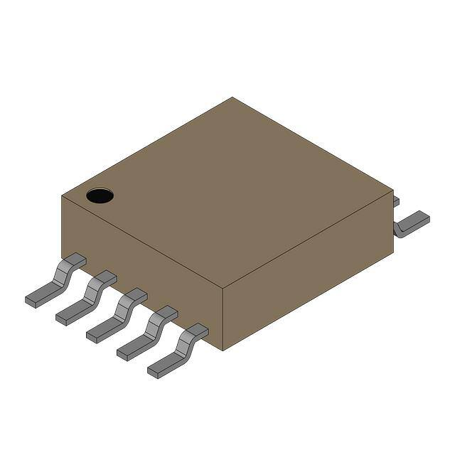
Connection Diagram
10LD Ceramic SOIC
20182202
Top View
See NS Package Number WG10A
© 2010 National Semiconductor Corporation
201822
www.national.com
LMP2012QML Dual Quad High Precision, Rail-to-Rail Output Operational Amplifier
November 30, 2010
�LMP2012QML
Absolute Maximum Ratings (Note 1)
Supply Voltage
Differential Input Voltage
Power Dissipation (Note 2)
Maximum Junction Temperature (TJmax)
Common-Mode Input Voltage
5.8V
±Supply Voltage
714mW
150°C
-0.3 ≤ VCM ≤ VCC +0.3V
30 mA
30 mA
50 mA
-55°C to +125°C
-55°C to +150°C
+260°C
Current at Input Pin
Current at Output Pin
Current at Power Supply Pin
Operating Temperature Range
Storage Temperature Range
Ceramic SOIC Lead Temperature (soldering 10 sec.)
Thermal Resistance
θJA
Ceramic SOIC (Still Air)
Ceramic SOIC (500LF/Min Air Flow)
175°C/W
115°C/W
θJC
Ceramic SOIC
Package Weight
Ceramic SOIC
ESD Tolerance (Note 3)
12.3°C/W
220mg
4000V
Quality Conformance Inspection
Mil-Std-883, Method 5005 - Group A
www.national.com
Subgroup
Description
Temp (°C)
1
Static tests at
+25
2
Static tests at
+125
3
Static tests at
-55
4
Dynamic tests at
+25
5
Dynamic tests at
+125
6
Dynamic tests at
-55
7
Functional tests at
+25
8A
Functional tests at
+125
8B
Functional tests at
-55
9
Switching tests at
+25
10
Switching tests at
+125
11
Switching tests at
-55
12
Setting time at
+25
13
Setting time at
+125
14
Setting time at
-55
2
�LMP2012QML
LMP2012 Electrical Characteristics
2.7V DC Parameters
The following conditions apply, unless otherwise specified.
V+ = 2.7V, V- = 0V, V CM = 1.35V, VO = 1.35V and RL > 1 MΩ.
Symbol
VIO
Parameter
Conditions
Notes
Typ
(Note 4)
Min
Max
0.8
Input Offset Voltage
36
Offset Calibration Time
10
Input Offset Voltage
(Temperature Sensitivity)
IIB
IIO
CMRR
Common Mode Rejection Ratio −0.3 ≤ VCM ≤ 0.9V
1
2, 3
0.015
µV/°C
Input Bias Current
−3
pA
Input Offset Current
6
pA
130
0 ≤ VCM ≤ 0.9V
95
Power Supply Rejection Ratio
120
AVOL
Open Loop Voltage Gain
130
95
124
RL = 2 kΩ
Output Swing
2.68
1
2, 3
95
1
90
2, 3
dB
90
1
85
2, 3
2.64
1
2.63
RL = 10 kΩ to 1.35V
VIN(diff) = ±0.5V
2, 3
dB
90
RL = 10 kΩ
1
dB
90
PSRR
VO
2, 3
ms
12
TCVIO
1
μV
60
0.5
Subgroups
Units
0.033
0.060
2, 3
V
1
0.075
2.65
RL = 2 kΩ to 1.35V
VIN(diff) = ±0.5V
2,3
2.615
1
2.6
2, 3
0.061
0.085
V
1
0.105
IO
Output Current
IS
Sourcing, VO = 0V
VIN(diff) = ±0.5V
12
Sinking, VO = 5V
VIN(diff) = ±0.5V
18
2, 3
5
1
3
2, 3
mA
5
1
3
2, 3
0.919
Supply Current per Channel
1.20
1.50
1
mA
2, 3
2.7V AC Parameters
The following conditions apply, unless otherwise specified.
V+ = 2.7V, V - = 0V, VCM = 1.35V, VO = 1.35V, and RL > 1 MΩ.
Symbol
Parameter
Conditions
Notes
Typ
(Note 4)
Min
Max
Units
Subgroups
1
5
MHz
4
GBW
Gain-Bandwidth Product
3
SR
Slew Rate
4
V/μs
θm
Phase Margin
60
Deg
Gm
Gain Margin
−14
dB
en
Input-Referred Voltage Noise
35
enP-P
Input-Referred Voltage Noise
trec
Input Overload Recovery Time
RS = 100Ω, DC to 10 Hz
3
nV/
850
nVPP
50
ms
www.national.com
�LMP2012QML
2.7V DC Parameters – 50 krad(Si) Post Radiation Limits @ +25°C
(Note 5)
The following conditions apply, unless otherwise specified.
V+ = 2.7V, V - = 0V, VCM = 1.35V, VO = 1.35V, and RL > 1 MΩ.
Symbol
IS
Parameter
Conditions
Notes
Supply Current per Channel
Typ
Min
Max
Units
Subgroups
1.75
mA
1
2.7V Operating Life Test Delta Parameters TA = +25°C
This is worst case drift, deltas are performed at room temperature post operation life. All other parameters, no deltas required.
Symbol
VIO
www.national.com
Parameter
Input offset voltage
Conditions
2.7 V
4
Limit
Units
±2
μV
�The following conditions apply, unless otherwise specified.
V+ = 5V, V- = 0V, V CM = 2.5V, VO = 2.5V and RL > 1MΩ.
Symbol
VIO
Parameter
Conditions
Notes
Typ
(Note 4)
Input Offset Voltage
0.12
Offset Calibration Time
0.5
Min
Max
36
60
10
12
TCVIO
Input Offset Voltage
(Temperature Sensitivity)
IIB
IIO
CMRR
Common Mode Rejection Ratio
Input Bias Current
−3
pA
Input Offset Current
6
pA
−0.3 ≤ VCM ≤ 3.2
130
100
90
Power Supply Rejection Ratio
120
Open Loop Voltage Gain
RL = 10 kΩ
130
RL = 2 kΩ
132
Output Swing
RL = 10 kΩ to 2.5V
VIN(diff) = ±0.5V
4.978
95
dB
105
dB
IS
15
Sourcing, VO = 5V
VIN(diff) = ±0.5V
17
0.080
V
0.930
1
2, 3
1
4.875
1
4.855
2, 3
0.125
V
1
2, 3
8
1
6
2, 3
mA
8
1
2, 3
1.20
1.50
5
2, 3
2, 3
6
Supply Current per Channel
1
2, 3
1
0.150
Sourcing, VO = 0V
VIN(diff) = ±0.5V
2, 3
4.92
0.091
Output Current
1
2, 3
2, 3
0.095
IO
2, 3
90
4.91
4.919
1
1
95
0.040
RL = 2 kΩ to 2.5V
VIN(diff) = ±0.5V
Subgroups
1
dB
100
VO
ms
µV/°C
90
AVOL
μV
0.015
0 ≤ VCM ≤ 3.2
PSRR
Units
mA
1
2, 3
www.national.com
LMP2012QML
5V DC Parameters
�LMP2012QML
5V AC Parameters
The following conditions apply, unless otherwise specified.
V+ = 5V, V - = 0V, VCM = 2.5V, VO = 2.5V, and RL > 1 MΩ.
Symbol
Parameter
Conditions
Notes
Typ
(Note 4)
Min
Max
Units
Subgroups
3
1
5
MHz
4
GBW
Gain-Bandwidth Product
SR
Slew Rate
4
V/μs
θm
Phase Margin
60
Deg
Gm
Gain Margin
−15
dB
en
Input-Referred Voltage Noise
enP-P
Input-Referred Voltage Noise
trec
Input Overload Recovery Time
35
RS = 100Ω, DC to 10 Hz
nV/
850
nVPP
50
ms
5V DC Parameters – 50 krad(Si) Post Radiation Limits @ +25°C
(Note 5)
The following conditions apply, unless otherwise specified.
V+ = 5V, V - = 0V, VCM = 2.5V, VO = 2.5V, and RL > 1 MΩ.
Symbol
IS
Parameter
Conditions
Notes
Typ
Supply Current per Channel
Min
Max
Units
Subgroups
1.75
mA
1
5V Operating Life Test Delta Parameters TA = +25°C
This is worst case drift, deltas are performed at room temperature post operation life. All other parameters, no deltas required.
Symbol
VIO
Parameter
Input offset voltage
Conditions
5.0 V
Limit
Units
±2
μV
Note 1: Absolute Maximum Ratings indicate limits beyond which damage to the device may occur. Operating Ratings indicate conditions for which the device is
functional, but do not guarantee specific performance limits. For guaranteed specifications and test conditions, see the Electrical Characteristics. The guaranteed
specifications apply only for the test conditions listed. Some performance characteristics may degrade when the device is not operated under the listed test
conditions.
Note 2: The maximum power dissipation must be derated at elevated temperatures and is dictated by TJmax (maximum junction temperature), θJA (package
junction to ambient thermal resistance), and TA (ambient temperature). The maximum allowable power dissipation at any temperature is PDmax = (TJmax - TA)/
θJA or the number given in the Absolute Maximum Ratings, whichever is lower.
Note 3: Human body model, 1.5 kΩ in series with 100 pF.
Note 4: Typical values represent the most likely parametric norm.
Note 5: Pre and post irradiation limits are identical to those listed under DC Parameters, except those listed in the Post Radiation Limit tables.
www.national.com
6
�THE BENEFITS OF LMP2012
NO 1/f NOISE
Using patented methods, the LMP2012 eliminates the 1/f
noise present in other amplifiers. That noise, which increases
as frequency decreases, is a major source of measurement
error in all DC-coupled measurements. Low-frequency noise
appears as a constantly-changing signal in series with any
measurement being made. As a result, even when the measurement is made rapidly, this constantly-changing noise signal will corrupt the result. The value of this noise signal can
be surprisingly large. For example: If a conventional amplifier
and a noise corner of
has a flat-band noise level of 10nV/
10 Hz, the RMS noise at 0.001 Hz is 1µV/
. This is equivalent to a 0.50 µV peak-to-peak error, in the frequency range
0.001 Hz to 1.0 Hz. In a circuit with a gain of 1000, this produces a 0.50 mV peak-to-peak output error. This number of
0.001 Hz might appear unreasonably low, but when a data
acquisition system is operating for 17 minutes, it has been on
long enough to include this error. In this same time, the
LMP2012 will only have a 0.21 mV output error. This is smaller
by 2.4 x. Keep in mind that this 1/f error gets even larger at
lower frequencies. At the extreme, many people try to reduce
this error by integrating or taking several samples of the same
signal. This is also doomed to failure because the 1/f nature
of this noise means that taking longer samples just moves the
measurement into lower frequencies where the noise level is
even higher.
The LMP2012 eliminates this source of error. The noise level
is constant with frequency so that reducing the bandwidth reduces the errors caused by noise.
NO EXTERNAL CAPACITORS REQUIRED
The LMP2012 does not need external capacitors. This eliminates the problems caused by capacitor leakage and dielectric absorption, which can cause delays of several seconds
from turn-on until the amplifier's error has settled.
MORE BENEFITS
The LMP2012 offers the benefits mentioned above and more.
It has a rail-to-rail output and consumes only 950 µA of supply
current while providing excellent DC and AC electrical performance. In DC performance, the LMP2012 achieves 130 dB
of CMRR, 120 dB of PSRR and 130 dB of open loop gain. In
AC performance, the LMP2012 provides 3 MHz of gain-bandwidth product and 4 V/µs of slew rate.
HOW THE LMP2012 WORKS
The LMP2012 uses new, patented techniques to achieve the
high DC accuracy traditionally associated with chopper-stabilized amplifiers without the major drawbacks produced by
chopping. The LMP2012 continuously monitors the input offset and corrects this error. The conventional chopping process produces many mixing products, both sums and
differences, between the chopping frequency and the incoming signal frequency. This mixing causes large amounts of
distortion, particularly when the signal frequency approaches
the chopping frequency. Even without an incoming signal, the
chopper harmonics mix with each other to produce even more
trash. If this sounds unlikely or difficult to understand, look at
the plot (Figure 2), of the output of a typical (MAX432) chopper-stabilized op amp. This is the output when there is no
incoming signal, just the amplifier in a gain of -10 with the input
grounded. The chopper is operating at about 150 Hz; the rest
is mixing products. Add an input signal and the noise gets
much worse. Compare this plot with Figure 3 of the LMP2012.
This data was taken under the exact same conditions. The
auto-zero action is visible at about 30 kHz but note the absence of mixing products at other frequencies. As a result, the
LMP2012 has very low distortion of 0.02% and very low mixing products.
OVERLOAD RECOVERY
The LMP2012 recovers from input overload much faster than
most chopper-stabilized op amps. Recovery from driving the
amplifier to 2X the full scale output, only requires about 40
ms. Many chopper-stabilized amplifiers will take from 250 ms
to several seconds to recover from this same overload. This
is because large capacitors are used to store the unadjusted
offset voltage.
20182216
FIGURE 1.
The wide bandwidth of the LMP2012 enhances performance
when it is used as an amplifier to drive loads that inject transients back into the output. ADCs (Analog-to-Digital Converters) and multiplexers are examples of this type of load. To
simulate this type of load, a pulse generator producing a 1V
peak square wave was connected to the output through a 10
pF capacitor. (Figure 1) The typical time for the output to recover to 1% of the applied pulse is 80 ns. To recover to 0.1%
requires 860ns. This rapid recovery is due to the wide bandwidth of the output stage and large total GBW.
20182217
FIGURE 2.
7
www.national.com
LMP2012QML
Application Information
�LMP2012QML
PRECISION STRAIN-GAUGE AMPLIFIER
This Strain-Gauge amplifier (Figure 4) provides high gain
(1006 or ~60 dB) with very low offset and drift. Using the resistors' tolerances as shown, the worst case CMRR will be
greater than 108 dB. The CMRR is directly related to the resistor mismatch. The rejection of common-mode error, at the
output, is independent of the differential gain, which is set by
R3. The CMRR is further improved, if the resistor ratio matching is improved, by specifying tighter-tolerance resistors, or
by trimming.
20182204
FIGURE 3.
INPUT CURRENTS
The LMP2012's input currents are different than standard
bipolar or CMOS input currents in that it appears as a current
flowing in one input and out the other. Under most operating
conditions, these currents are in the picoamp level and will
have little or no effect in most circuits. These currents tend to
increase slightly when the common-mode voltage is near the
minus supply. At high temperatures, the input currents become larger, 0.5 nA typical, and are both positive except when
the VCM is near V−. If operation is expected at low commonmode voltages and high temperature, do not add resistance
in series with the inputs to balance the impedances. Doing
this can cause an increase in offset voltage. A small resistance such as 1 kΩ can provide some protection against very
large transients or overloads, and will not increase the offset
significantly.
www.national.com
20182218
FIGURE 4.
Extending Supply Voltages and Output Swing by Using a
Composite Amplifier Configuration:
In cases where substantially higher output swing is required
with higher supply voltages, arrangements like the ones
shown in Figure 5 and Figure 6 could be used. These configurations utilize the excellent DC performance of the LMP2012
while at the same time allow the superior voltage and frequency capabilities of the LM6171 to set the dynamic performance of the overall amplifier. For example, it is possible to
achieve ±12V output swing with 300 MHz of overall GBW
(AV = 100) while keeping the worst case output shift due to
VOS less than 4 mV. The LMP2012 output voltage is kept at
about mid-point of its overall supply voltage, and its input
common mode voltage range allows the V- terminal to be
grounded in one case (Figure 5, inverting operation) and tied
to a small non-critical negative bias in another (Figure 6, noninverting operation). Higher closed-loop gains are also possible with a corresponding reduction in realizable bandwidth.
Table 1 shows some other closed loop gain possibilities along
with the measured performance in each case.
8
�LMP2012QML
20182219
20182220
FIGURE 5.
FIGURE 6.
TABLE 1. Composite Amplifier Measured Performance
AV
R1
Ω
R2
Ω
C2
pF
BW
MHz
SR
(V/μs)
en p-p
(mVPP)
50
200
10k
8
3.3
178
37
100
100
10k
10
2.5
174
70
100
1k
100k
0.67
3.1
170
70
500
200
100k
1.75
1.4
96
250
1000
100
100k
2.2
0.98
64
400
It should be kept in mind that in order to minimize the output
noise voltage for a given closed-loop gain setting, one could
minimize the overall bandwidth. As can be seen from Equation 1 above, the output noise has a square-root relationship
to the Bandwidth.
In the case of the inverting configuration, it is also possible to
increase the input impedance of the overall amplifier, by raising the value of R1, without having to increase the feed-back
resistor, R2, to impractical values, by utilizing a "Tee" network
as feedback. See the LMC6442 data sheet (Application Notes
section) for more details on this.
In terms of the measured output peak-to-peak noise, the following relationship holds between output noise voltage, en pp, for different closed-loop gain, AV, settings, where −3 dB
Bandwidth is BW:
20182221
FIGURE 7.
9
www.national.com
�LMP2012QML
Op amp flatband noise = 8nV/
1/f corner frequency = 100 Hz
AV = 2000
Measurement time = 100 sec
Bandwidth = 2 Hz
This example will result in about 2.2 mVPP (1.9 LSB) of
output noise contribution due to the op amp alone, compared to about 594 μVPP (less than 0.5 LSB) when that
op amp is replaced with the LMP2012 which has no 1/f
contribution. If the measurement time is increased from
100 seconds to 1 hour, the improvement realized by using
the LMP2012 would be a factor of about 4.8 times (2.86
mVPP compared to 596 μV when LMP2012 is used) mainly because the LMP2012 accuracy is not compromised
by increasing the observation time.
D) Rail-to-Rail output swing maximizes the ADC dynamic
range in 5-Volt single-supply converter applications. Below are some typical block diagrams showing the
LMP2012 used as an ADC amplifier (Figure 7 and Figure
8).
LMP2012 AS ADC INPUT AMPLIFIER
The LMP2012 is a great choice for an amplifier stage immediately before the input of an ADC (Analog-to-Digital Converter), whether AC or DC coupled. See Figure 7 and Figure
8. This is because of the following important characteristics:
A) Very low offset voltage and offset voltage drift over time
and temperature allow a high closed-loop gain setting
without introducing any short-term or long-term errors.
For example, when set to a closed-loop gain of 100 as the
analog input amplifier for a 12-bit A/D converter, the overall conversion error over full operation temperature and
30 years life of the part (operating at 50°C) would be less
than 5 LSBs.
B) Fast large-signal settling time to 0.01% of final value (1.4
μs) allows 12 bit accuracy at 100 KHZ or more sampling
rate.
C) No flicker (1/f) noise means unsurpassed data accuracy
over any measurement period of time, no matter how
long. Consider the following op amp performance, based
on a typical low-noise, high-performance commerciallyavailable device, for comparison:
20182222
FIGURE 8.
than 0.082 rad(Si)/s. Wafer level TID data are available with
lot shipments.
RADIATION ENVIRONMENTS
Careful consideration should be given to environmental conditions when using a product in a radiation environment.
ELDRS-FREE PRODUCTS
ELDRS-Free products are tested and qualified on a wafer
level basis at a dose rate of 10 mrad(Si)/s per MIL-STD-883G,
Test Method 1019.7, Condition D. Wafer level low dose rate
test data are available with lot shipments.
TOTAL IONIZING DOSE
Radiation hardness assured (RHA) products are those part
numbers with a total ionizing dose (TID) level specified in the
Ordering Information table on the front page. Testing and
qualification of these products is done on a wafer level according to MIL-STD-883G, Test Method 1019.7, Condition A
and the “Extended room temperature anneal test” described
in section 3.11 for application environment dose rates less
www.national.com
SINGLE EVENT UPSET
A report on single event upset (SEU) is available upon request.
10
�Date Released
Revision
Section
03/19/07
A
Initial Release
Changes
10/17/08
B
Electrical Section
07/13/09
C
2.7V DC and 5V DC Electrical Section
Added typical parameter TCVOS to 2.7V DC and 5V
DC Electrical Section. Revision B will be Archived.
12/08/09
D
Features, Ordering Information and Notes
Reference to ELDRS, New ELDRS part number and
added ELDRS Note 6. Revision C will be Archived.
06/08/2010
E
General Description, 2.7V DC and 5V DC
Electrical Section added New Radiation
Section.
Removed first line. Added Delta Table to Electrical's
to match what is in the SMD and New Radiation
Section. Revision D will be Archived.
11/30/2010
F
AC Electrical 5V parameter table conditions Correct typo to unless otherwise specified
parameters From: V+ = 2.7V, V - = 0V, VCM = 1.35V,
Initial Release
Added typical parameters to 2.7V and 5V AC
Electrical Sections. Revision A will be Archived.
VO = 1.35V, and RL > 1 MΩ. To: V+ = 5V, V - = 0V,
VCM = 2.5V, VO = 2.5V, and RL > 1 MΩ. Revision E
will be Archived.
11
www.national.com
LMP2012QML
Revision History
�LMP2012QML
Physical Dimensions inches (millimeters) unless otherwise noted
10-Pin Ceramic SOIC
NS Package Number WG10A
www.national.com
12
�LMP2012QML
Notes
13
www.national.com
�LMP2012QML Dual Quad High Precision, Rail-to-Rail Output Operational Amplifier
Notes
For more National Semiconductor product information and proven design tools, visit the following Web sites at:
www.national.com
Products
Design Support
Amplifiers
www.national.com/amplifiers
WEBENCH® Tools
www.national.com/webench
Audio
www.national.com/audio
App Notes
www.national.com/appnotes
Clock and Timing
www.national.com/timing
Reference Designs
www.national.com/refdesigns
Data Converters
www.national.com/adc
Samples
www.national.com/samples
Interface
www.national.com/interface
Eval Boards
www.national.com/evalboards
LVDS
www.national.com/lvds
Packaging
www.national.com/packaging
Power Management
www.national.com/power
Green Compliance
www.national.com/quality/green
Switching Regulators
www.national.com/switchers
Distributors
www.national.com/contacts
LDOs
www.national.com/ldo
Quality and Reliability
www.national.com/quality
LED Lighting
www.national.com/led
Feedback/Support
www.national.com/feedback
Voltage References
www.national.com/vref
Design Made Easy
www.national.com/easy
www.national.com/powerwise
Applications & Markets
www.national.com/solutions
Mil/Aero
www.national.com/milaero
PowerWise® Solutions
Serial Digital Interface (SDI) www.national.com/sdi
Temperature Sensors
www.national.com/tempsensors SolarMagic™
www.national.com/solarmagic
PLL/VCO
www.national.com/wireless
www.national.com/training
PowerWise® Design
University
THE CONTENTS OF THIS DOCUMENT ARE PROVIDED IN CONNECTION WITH NATIONAL SEMICONDUCTOR CORPORATION
(“NATIONAL”) PRODUCTS. NATIONAL MAKES NO REPRESENTATIONS OR WARRANTIES WITH RESPECT TO THE ACCURACY
OR COMPLETENESS OF THE CONTENTS OF THIS PUBLICATION AND RESERVES THE RIGHT TO MAKE CHANGES TO
SPECIFICATIONS AND PRODUCT DESCRIPTIONS AT ANY TIME WITHOUT NOTICE. NO LICENSE, WHETHER EXPRESS,
IMPLIED, ARISING BY ESTOPPEL OR OTHERWISE, TO ANY INTELLECTUAL PROPERTY RIGHTS IS GRANTED BY THIS
DOCUMENT.
TESTING AND OTHER QUALITY CONTROLS ARE USED TO THE EXTENT NATIONAL DEEMS NECESSARY TO SUPPORT
NATIONAL’S PRODUCT WARRANTY. EXCEPT WHERE MANDATED BY GOVERNMENT REQUIREMENTS, TESTING OF ALL
PARAMETERS OF EACH PRODUCT IS NOT NECESSARILY PERFORMED. NATIONAL ASSUMES NO LIABILITY FOR
APPLICATIONS ASSISTANCE OR BUYER PRODUCT DESIGN. BUYERS ARE RESPONSIBLE FOR THEIR PRODUCTS AND
APPLICATIONS USING NATIONAL COMPONENTS. PRIOR TO USING OR DISTRIBUTING ANY PRODUCTS THAT INCLUDE
NATIONAL COMPONENTS, BUYERS SHOULD PROVIDE ADEQUATE DESIGN, TESTING AND OPERATING SAFEGUARDS.
EXCEPT AS PROVIDED IN NATIONAL’S TERMS AND CONDITIONS OF SALE FOR SUCH PRODUCTS, NATIONAL ASSUMES NO
LIABILITY WHATSOEVER, AND NATIONAL DISCLAIMS ANY EXPRESS OR IMPLIED WARRANTY RELATING TO THE SALE
AND/OR USE OF NATIONAL PRODUCTS INCLUDING LIABILITY OR WARRANTIES RELATING TO FITNESS FOR A PARTICULAR
PURPOSE, MERCHANTABILITY, OR INFRINGEMENT OF ANY PATENT, COPYRIGHT OR OTHER INTELLECTUAL PROPERTY
RIGHT.
LIFE SUPPORT POLICY
NATIONAL’S PRODUCTS ARE NOT AUTHORIZED FOR USE AS CRITICAL COMPONENTS IN LIFE SUPPORT DEVICES OR
SYSTEMS WITHOUT THE EXPRESS PRIOR WRITTEN APPROVAL OF THE CHIEF EXECUTIVE OFFICER AND GENERAL
COUNSEL OF NATIONAL SEMICONDUCTOR CORPORATION. As used herein:
Life support devices or systems are devices which (a) are intended for surgical implant into the body, or (b) support or sustain life and
whose failure to perform when properly used in accordance with instructions for use provided in the labeling can be reasonably expected
to result in a significant injury to the user. A critical component is any component in a life support device or system whose failure to perform
can be reasonably expected to cause the failure of the life support device or system or to affect its safety or effectiveness.
National Semiconductor and the National Semiconductor logo are registered trademarks of National Semiconductor Corporation. All other
brand or product names may be trademarks or registered trademarks of their respective holders.
Copyright© 2010 National Semiconductor Corporation
For the most current product information visit us at www.national.com
National Semiconductor
Americas Technical
Support Center
Email: support@nsc.com
Tel: 1-800-272-9959
www.national.com
National Semiconductor Europe
Technical Support Center
Email: europe.support@nsc.com
National Semiconductor Asia
Pacific Technical Support Center
Email: ap.support@nsc.com
National Semiconductor Japan
Technical Support Center
Email: jpn.feedback@nsc.com
�