User’s Guide
March 2013
LMP8480 / 81 EVM User’s Guide
CONTENTS
1.
INTRODUCTION ................................................................................................ 3
2.
FEATURES ........................................................................................................ 3
3.
BOARD CONNECTIONS AND COMPONENTS ................................................. 4
3.1. GENERAL SAFETY PRECAUTIONS ................................................................. 4
3.2. POWER SUPPLY INPUT - VCC ......................................................................... 4
3.3. CURRENT SENSE RESISTOR AND SENSE TERMINALS - RSP AND RSN ..... 4
3.4. OPTIONAL INPUT FILTERING .......................................................................... 5
3.5. REFERENCE INPUTS (BI-DIRECTIONAL DEVICES ONLY) ............................. 6
3.6. OUTPUT - VOUT ............................................................................................... 6
3.7. INPUT VSENSE TEST POINT – TP1 ................................................................. 7
3.8. DUT MOUNTING OPTIONS ............................................................................... 7
March 2013
4.
BOARD TEST PROCEDURE FOR UNI-DIRECTIONAL DEVICES (LMP8480-S) 8
5.
BOARD TEST PROCEDURE FOR BI-DIRECTIONAL DEVICES (LMP8481-S) .. 9
6.
SCHEMATIC .................................................................................................... 10
7.
BILL OF MATERIALS ....................................................................................... 11
LMP8480/81 User’s Guide SNOU031A
1
�User’s Guide
March 2013
LMP8480 / 81 EVM User’s Guide
LIST OF FIGURES
Figure 1: Picture of Evaluation Board (LMP8480 version) ........................................................................................... 3
Figure 2: Rsense Terminals .......................................................................................................................................... 4
Figure 3: Cutting pads to accommodate 4-wire resistors ............................................................................................. 5
Figure 4: Rt shorting traces must be cut before use ..................................................................................................... 5
Figure 5: Optional Input Filtering Capacitors ................................................................................................................ 5
Figure 6: Optional Riso and Shorting Pad .................................................................................................................... 6
Figure 7: Reference Jumper Pins ................................................................................................................................. 6
Figure 8: Setup for Uni-Directional Devices .................................................................................................................. 8
Figure 9: Setup for Bi-Directional Devices .................................................................................................................... 9
Figure 10: EVM Schematic ......................................................................................................................................... 10
LIST OF TABLES
Table 1: Reference Jumper Settings ............................................................................................................................ 6
Table 2: Bill of Materials .............................................................................................................................................. 11
March 2013
LMP8480/81 User’s Guide SNOU031A
2
�User’s Guide
March 2013
LMP8480 / 81 EVM User’s Guide
1. Introduction
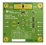
The Texas Instruments LMP8480/81 evaluation module (EVM) helps designers quickly evaluate the
operation and performance of the LMP8480/81 76V Precision High Side Current Sense Amplifiers. The EVM
is ready to connect to power, load, and test instruments through the use of on-board terminals.
Figure 1: Picture of Evaluation Board (LMP8480 version)
The EVM contains one LMP8480 or LMP8481 high side evaluation circuit. The EVM’s come pre-assembled
with the LMP8480/81 device, 0.1Ω sense resistor; bypass capacitor and connection terminals installed. The
Bi-Directional EVM’s include the JP1 and JP2 reference jumpers and terminals.
2. Features
•
•
•
•
•
•
March 2013
Selectable reference voltage options through jumpers (LMP8481)
On-board sense resistor or external resistor
Optional input EMI/RFI filtering
Separate DUT and load supplies
Sense voltage test points
Optional output isolation resistor
LMP8480/81 User’s Guide SNOU031A
3
�Setup
3. Board Connections and Components
This section describes the jumpers and connectors on the EVM as well and how to properly connect, set up
the EVM board.
3.1. General Safety Precautions
Connections with 48V or 1A and above should be securely soldered to the terminals to prevent inadvertent
disconnection. Voltages above 70V must be soldered. Clip-on leads are not recommended at high voltages.
Follow all standard high voltage precautions.
All power should be removed when changing connections, even in the low voltage sections. The use of handheld probes while powered is not recommended. Connections should be hard wired.
3.2. Power Supply Input - VCC
The device power supply is connected to the VCC and GND pins. Positions for 4.7uF (optional) and 0.1uF
ceramic bypass capacitors are provided on the VCC lines. Note that these capacitors should be rated for
100V or more. EVM supply voltage is limited to 75V max.
3.3. Current Sense Resistor and Sense Terminals - RSP and RSN
The large current sense resistor pads allow for multiple mounting configurations of both through-hole and
surface mount resistors.
WARNING: The area around the sense resistor can get warm. Use caution when handling or probing.
Figure 2: Rsense Terminals
These pads are bare copper to allow for mounting of any size or shape of resistor, as well as providing heat
dissipation. The larger inner holes are for optional pin socket receptacles (see Bill of Materials) to allow easy
swapping of through-hole resistors for prototyping.
Customer provided sense resistor power dissipation should be limited to less than 1W. The TI supplied 0.1
Ohm resistor power dissipation must be less than 0.5W. Currents higher than 5A should be soldered directly
to the sense pads. Currents above 10A should use an off-board shunt resistor with its own heat sink.
For off-board current sense resistors, the sense lines can be connected to the SENSE+ and SENSE- turret
terminals (with on-board sense resistor removed). It is recommended that these wires be twisted to prevent
noise pickup and to provide some EMI rejection.
4
LMP8480/81 User’s Guide
March 2013
�Setup
For 4-wire, or “Kelvin” resistors, Figure 2 shows how the sense traces can be cut with an E-Xacto knife to
attach to the “sense” terminals on a 4-Wire surface mount resistor.
Figure 3: Cutting pads to accommodate 4-wire resistors
Load ground currents should be kept off the board. Load current should be returned directly to the power
supply terminals and not through the demo board grounds.
3.4. Optional Input Filtering
The optional Rt+ and Rt- resistor pads are provided to add, in conjunction with C3, C4 and C5, EMI/Noise
filtering to the input. These can be series resistors or inductors. To maintain a continuous solid copper path,
the Rt pads have shorting traces across them. To use these pads, the shorting traces must be be cut before
installing Rt.
Figure 4: Rt shorting traces must be cut before use
To maintain accuracy, these resistors should be of equal value and well matched, as they are in series with
the device’s internal thin-film resistors and will effect the Gain, CMRR and gain accuracy specifications. The
values of these resistors should not exceed a few hundred ohms, and should be kept as low as possible.
Figure 5: Optional Input Filtering Capacitors
Pads C3, C4 and C5 are provided for optional EMI rejection. For RF/EMI protection, values in the 10 to
100pF range are recommended. For lower frequencies, a lowpass filter can be formed with the Rt series
input resistors.
March 2013
Literature Number SNOU031A
5
�Setup
3.5.
Reference Inputs (Bi-Directional Devices Only)
For Bi-Directional devices, the “zero” output level can be set by a voltage applied to the reference pins. The
reference voltages may be applied externally through the VREF pin, or sourced from the VCC line. These
jumpers will have no effect on devices without reference pins!!!
C6 and C7 are available if reference line bypassing or filtering is desired.
Figure 6: Reference Jumper Pins
Table 1 below shows the jumper positions and the input configuration.
Jumper Position
Reference
JP1
JP2
1-2
1-2
2-3
1-2
2-3
1-2
VREF
VREF / 2
(VS + VREF) / 2
2-3
2-3
VS / 2
Table 1: Reference Jumper Settings
3.6. Output - VOUT
Similar to the Rt resistors, Riso is available for output isolation when driving capacitive loads or for output
short circuit protection. If the output must drive large capacitive loads (like a coax cable), Riso may be
needed to prevent oscillations. The jumper trace between the pads must be cut to use Riso.
Figure 7: Optional Riso and Shorting Pad
6
LMP8480/81 User’s Guide
March 2013
�Setup
3.7. Input VSENSE Test Point – TP1
TP1 allows for the monitoring of the VSENSE voltage through a standard 0.1” header. TP2 provides a
convenient ground if needed. The meters terminals need to be “floating” (not grounded) and will be at the
common mode voltage (Vsource) potential.
3.8.
DUT Mounting Options
For applications where the DUT must be swapped-out, mounting holes are provided for a reusable “Rainbow
Clamp” socket from Rainbow Labs (See Bill of Materials). Otherwise, the DUT may be soldered directly to the
pads.
March 2013
Literature Number SNOU031A
7
�4. Board Test Procedure for Uni-Directional Devices (LMP8480-S)
Required Equipment:
•
•
•
•
1 ea. 20V, >1A power supply
2 ea. 4.5 digit or better DMM (Agilent 34401 or equiv)
1 ea. 20 ohm, >25W power resistor or programmable load sinking 1A.
Misc test leads for connections.
Connect board as shown, but do not connect SENSE- to load yet.
1.
2.
3.
4.
5.
6.
7.
8.
9.
10.
Connect 20V power supply as VSOURCE (turn off power for now).
Connect DMM1 to the output and ground terminals (+ to output, - to GND)
Connect DMM2 to the TP1 terminals or sense terminals (+ to RSP, - to RSN)
Confirm SENSE- is not connected and turn on power.
DMM1 should be between 0V and 5.5mV.
Now connect RLOAD to SENSE- as shown.
Record reading from DMM1 (should be around 6V for the “S” device)
Record reading from DMM2 (should be around 100mV – depending on accuracy of RLOAD)
The reading of DMM1 should be within 0.1% of the gain (60 for “S” version) times the DMM2 reading.
Turn off Vsource or disconnect RLOAD to prevent excessive heating.
Keep in mind that heating of the load and sense resistors may cause drift between steps 7 and 8. DMM
measurements should be taken quickly or simultaneously (use manual trigger function to trigger the readings
at the same time).
VSOURCE
+
RLOAD
-
DMM 2
+DMM 1
+
-
Figure 8: Setup for Uni-Directional Devices
8
LMP8480/81 User’s Guide
March 2013
�5. Board Test Procedure for Bi-Directional Devices (LMP8481-S)
Required Equipment:
•
•
•
•
•
1 ea. 10V, >1A power supply
2 ea. 4.5 digit or better DMM (Agilent 34401 or equiv)
1 ea. 20 ohm, >20W power resistor or programmable load sinking 0.5A.
2 ea 0.1” Jumper blocks
Misc test leads for connections
Connect board as shown, but do not connect SENSE- to load yet.
1.
2.
3.
4.
5.
6.
7.
8.
9.
10.
Connect 10V power supply as VSOURCE (turn off power for now).
Connect DMM1 to the output and ground terminals (+ to output, - to GND)
Connect DMM2 to the TP1 terminals or sense terminals (+ to RSP, - to RSN)
Place jumpers across JP1 2&3 and JP2 2&3 to set reference to VS/2.
Confirm SENSE- (load) is not connected.
Turn on power and record DMM1 reading (should be 5V* - this is the VREF voltage).
Now connect RLOAD to SENSE- as shown.
Record reading from DMM1 (should be around 8V for the “S” device)
Record reading from DMM2 (should be around 50mV)
The difference in the two readings of DMM1 should be within 0.1% of device gain (60) times the
DMM2 reading plus the VREF reading in step 6.
11. Reverse the SENSE+ and SENSE- leads. DMM2 should measure -100mV and the output should be
at 3V for the “S” device.
12. Turn off Vsource or disconnect RLOAD to prevent excessive heating.
VSOURCE
+
RLOAD
-
DMM 2
+DMM 1
+
-
Figure 9: Setup for Bi-Directional Devices
March 2013
Literature Number SNOU031A
9
�6. Schematic
Figure 10: EVM Schematic
10
LMP8480/81 User’s Guide
March 2013
�7. Bill of Materials
Table 2: Bill of Materials
Designator
EVB
Current Sense Evaluation Board
†
C1
†
†
C2, C3 , C4 ,
†
C5
†
†
C6 , C7
†
C8
DUT1
†
†
H1 , H2 ,
†
†
H3 , H4
†
†
H5 , H6 ,
†
†
H7 , H8
J1, J2, J3,
‡
‡
J4, J5 , J6 ,
J7, J8
†
†
J9 , J10
‡
‡
JP1 , JP2
†
Riso
Rsense
†
†
Rt+ , Rt†
TP1
TP2
SKT
Description
†
CAP, CERM, 4.7uF, 100V, +/-20%, X7R,
2220
CAP, CERM, 0.1uF, 100V, +/-10%, X7R,
1206
CAP, CERM, 0.1uF, 25V, +/-10%, X7R, 0603
CAP, CERM, 1000pF, 100V, +/-5%,
C0G/NP0, 0603
76V Common Mode, Precision Current
Sensing Amplifier, 8-pin MSOP
Machine Screw, Round, #4-40 x 1/4, Nylon,
Philips panhead
Manufacturer
Texas
Instruments
PartNumber
551600825-001
TDK
C5750X7R2A475M
TDK
C3216X7R2A104K
TDK
C1608X7R1E104K
TDK
C1608C0G2A102J
Texas
Instruments
B&F Fastener
Supply
LMP8480MM-x or LMP8481MM-x
NY PMS 440 0025 PH
Standoff, Hex, 0.5"L #4-40 Nylon
Keystone
1902C
Terminal, Turret, TH, Double
Keystone
1593-2
Mill-Max
0328-0-15-15-34-27-10-0
Samtec Inc.
TSW-103-07-G-S
Panasonic
IRC
Yageo America
ERJ-6GEY0R00V
LRC-LR1206LF-01_R100_F
RC0603JR-070RL
Samtec Inc.
TSW-102-07-G-S
Keystone
Rainbow
Technologies
5011
PCB Socket, solderless Pressfit, Large, .032
to .046
Header, TH, 100mil, 3x1, Gold plated, 230
mil above insulator
RES, 0 ohm, 5%, 0.125W, 0805
RES, 0.1 ohm, 1%, 0.5W, 1210
RES, 0 ohm, 5%, 0.1W, 0603
Header, TH, 100mil, 2x1, Gold plated, 230
mil above insulator
Test Point, TH, Multipurpose, Black
8-PIN Mini-SO .118W Clamp Socket
MSO8SD
† User Option – not installed
‡ Installed on devices with reference pins
March 2013
Literature Number SNOU031A
11
�EVM Warnings and Restrictions
It is important to operate this EVM within the input voltage range of of 4.0V to +75V; a supply voltage (Vs) range of
+4.5V to +75V; and the output voltage range of GND + 0.05V to ( Vs – 0.4V or 13.6 – whichever is less). Total
dissipation of the TI installed sense resistor shall not exceed 0.5W. Turret terminals are rated for 5A max.
Exceeding the specified input range may cause unexpected operation and/or irreversible damage to the EVM. If
there are questions concerning the input range, please contact a TI field representative prior to connecting the input
power.
Applying loads outside of the specified output range may result in unintended operation and/or possible permanent
damage to the EVM. Please consult the EVM User's Guide prior to connecting any load to the EVM output. If there
is uncertainty as to the load specification, please contact a TI field representative.
During normal operation, some circuit components may have case temperatures greater than +25°C. The EVM is
designed to operate properly with certain components above +25°C as long as the input and output ranges are
maintained. These components include but are not limited to linear regulators, switching transistors, pass
transistors, and current sense resistors. These types of devices can be identified using the EVM schematic located
in the EVM User's Guide. When placing measurement probes near these devices during operation, please be
aware that these devices may be very warm to the touch.
EVALUATION BOARD/KIT/MODULE (EVM) ADDITIONAL TERMS
Texas Instruments (TI) provides the enclosed Evaluation Board/Kit/Module (EVM) under the following conditions:
The user assumes all responsibility and liability for proper and safe handling of the goods. Further, the user
indemnifies TI from all claims arising from the handling or use of the goods.
Should this evaluation board/kit not meet the specifications indicated in the User’s Guide, the board/kit may be
returned within 30 days from the date of delivery for a full refund. THE FOREGOING LIMITED WARRANTY IS THE
EXCLUSIVE WARRANTY MADE BY SELLER TO BUYER AND IS IN LIEU OF ALL OTHER WARRANTIES,
EXPRESSED, IMPLIED, OR STATUTORY, INCLUDING ANY WARRANTY OF MERCHANTABILITY OR FITNESS
FOR ANY PARTICULAR PURPOSE. EXCEPT TO THE EXTENT OF THE INDEMNITY SET FORTH ABOVE,
NEITHER PARTY SHALL BE LIABLE TO THE OTHER FOR ANY INDIRECT, SPECIAL, INCIDENTAL, OR
CONSEQUENTIAL DAMAGES.
Please read the User's Guide and, specifically, the Warnings and Restrictions notice in the User's Guide prior to
handling the product. This notice contains important safety information about temperatures and voltages. For
additional information on TI's environmental and/or safety programs, please visit www.ti.com/esh or contact TI.
No license is granted under any patent right or other intellectual property right of TI covering or relating to any
machine, process, or combination in which such TI products or services might be or are used. TI currently deals
with a variety of customers for products, and therefore our arrangement with the user is not exclusive. TI assumes
no liability for applications assistance, customer product design, software performance, or infringement of patents
or services described herein.
REGULATORY COMPLIANCE INFORMATION
As noted in the EVM User’s Guide and/or EVM itself, this EVM and/or accompanying hardware may or may not be
subject to the Federal Communications Commission (FCC) and Industry Canada (IC) rules.
12
LMP8480/81 User’s Guide
March 2013
�For EVMs not subject to the above rules, this evaluation board/kit/module is intended for use for ENGINEERING
DEVELOPMENT, DEMONSTRATION OR EVALUATION PURPOSES ONLY and is not considered by TI to be a
finished end product fit for general consumer use. It generates, uses, and can radiate radio frequency energy and
has not been tested for compliance with the limits of computing devices pursuant to part 15 of FCC or ICES-003
rules, which are designed to provide reasonable protection against radio frequency interference. Operation of the
equipment may cause interference with radio communications, in which case the user at his own expense will be
required to take whatever measures may be required to correct this interference.
General Statement for EVMs including a radio
User Power/Frequency Use Obligations: This radio is intended for development/professional use only in legally
allocated frequency and power limits. Any use of radio frequencies and/or power availability of this EVM and its
development application(s) must comply with local laws governing radio spectrum allocation and power limits for
this evaluation module. It is the user’s sole responsibility to only operate this radio in legally acceptable frequency
space and within legally mandated power limitations. Any exceptions to this are strictly prohibited and unauthorized
by Texas Instruments unless user has obtained appropriate experimental/development licenses from local
regulatory authorities, which is responsibility of user including its acceptable authorization.
For EVMs annotated as FCC – FEDERAL COMMUNICATIONS COMMISSION Part 15 Compliant
Caution
This device complies with part 15 of the FCC Rules. Operation is subject to the following two conditions: (1) This
device may not cause harmful interference, and (2) this device must accept any interference received, including
interference that may cause undesired operation.
Changes or modifications not expressly approved by the party responsible for compliance could void the user's
authority to operate the equipment.
FCC Interference Statement for Class A EVM devices
This equipment has been tested and found to comply with the limits for a Class A digital device, pursuant to part 15
of the FCC Rules. These limits are designed to provide reasonable protection against harmful interference when
the equipment is operated in a commercial environment. This equipment generates, uses, and can radiate radio
frequency energy and, if not installed and used in accordance with the instruction manual, may cause harmful
interference to radio communications. Operation of this equipment in a residential area is likely to cause harmful
interference in which case the user will be required to correct the interference at his own expense.
FCC Interference Statement for Class B EVM devices
This equipment has been tested and found to comply with the limits for a Class B digital device, pursuant to part 15
of the FCC Rules. These limits are designed to provide reasonable protection against harmful interference in a
residential installation. This equipment generates, uses and can radiate radio frequency energy and, if not installed
and used in accordance with the instructions, may cause harmful interference to radio communications. However,
there is no guarantee that interference will not occur in a particular installation. If this equipment does cause
harmful interference to radio or television reception, which can be determined by turning the equipment off and on,
the user is encouraged to try to correct the interference by one or more of the following measures:
•
•
•
•
Reorient or relocate the receiving antenna.
Increase the separation between the equipment and receiver.
Connect the equipment into an outlet on a circuit different from that to which the receiver is connected.
Consult the dealer or an experienced radio/TV technician for help.
March 2013
Literature Number SNOU031A
13
�For EVMs annotated as IC – INDUSTRY CANADA Compliant
This Class A or B digital apparatus complies with Canadian ICES-003.
Changes or modifications not expressly approved by the party responsible for compliance could void the user’s
authority to operate the equipment.
Concerning EVMs including radio transmitters
This device complies with Industry Canada licence-exempt RSS standard(s). Operation is subject to the following
two conditions: (1) this device may not cause interference, and (2) this device must accept any interference,
including interference that may cause undesired operation of the device.
Concerning EVMs including detachable antennas
Under Industry Canada regulations, this radio transmitter may only operate using an antenna of a type and
maximum (or lesser) gain approved for the transmitter by Industry Canada. To reduce potential radio interference to
other users, the antenna type and its gain should be so chosen that the equivalent isotropically radiated power
(e.i.r.p.) is not more than that necessary for successful communication.
This radio transmitter has been approved by Industry Canada to operate with the antenna types listed in the user
guide with the maximum permissible gain and required antenna impedance for each antenna type indicated.
Antenna types not included in this list, having a gain greater than the maximum gain indicated for that type, are
strictly prohibited for use with this device.
Cet appareil numérique de la classe A ou B est conforme à la norme NMB-003 du Canada.
Les changements ou les modifications pas expressément approuvés par la partie responsable de la conformité ont
pu vider l’autorité de l'utilisateur pour actionner l'équipement.
Concernant les EVMs avec appareils radio
Le présent appareil est conforme aux CNR d'Industrie Canada applicables aux appareils radio exempts de licence.
L'exploitation est autorisée aux deux conditions suivantes : (1) l'appareil ne doit pas produire de brouillage, et (2)
l'utilisateur de l'appareil doit accepter tout brouillage radioélectrique subi, même si le brouillage est susceptible d'en
compromettre le fonctionnement.
Concernant les EVMs avec antennes détachables
Conformément à la réglementation d'Industrie Canada, le présent émetteur radio peut fonctionner avec une
antenne d'un type et d'un gain maximal (ou inférieur) approuvé pour l'émetteur par Industrie Canada. Dans le but
de réduire les risques de brouillage radioélectrique à l'intention des autres utilisateurs, il faut choisir le type
d'antenne et son gain de sorte que la puissance isotrope rayonnée équivalente (p.i.r.e.) ne dépasse pas l'intensité
nécessaire à l'établissement d'une communication satisfaisante.
Le présent émetteur radio a été approuvé par Industrie Canada pour fonctionner avec les types d'antenne
énumérés dans le manuel d’usage et ayant un gain admissible maximal et l'impédance requise pour chaque type
d'antenne. Les types d'antenne non inclus dans cette liste, ou dont le gain est supérieur au gain maximal indiqué,
sont strictement interdits pour l'exploitation de l'émetteur.
SPACER
SPACER
SPACER
14
LMP8480/81 User’s Guide
March 2013
�【Important Notice for Users of this Product in Japan】
This development kit is NOT certified as Confirming to Technical Regulations of Radio Law of Japan
If you use this product in Japan, you are required by Radio Law of Japan to follow the instructions below with
respect to this product:
1. Use this product in a shielded room or any other test facility as defined in the notification #173 issued by
Ministry of Internal Affairs and Communications on March 28, 2006, based on Sub-section 1.1 of Article 6
of the Ministry’s Rule for Enforcement of Radio Law of Japan,
2. Use this product only after you obtained the license of Test Radio Station as provided in Radio Law of
Japan with respect to this product, or
3. Use of this product only after you obtained the Technical Regulations Conformity Certification as provided
in Radio Law of Japan with respect to this product. Also, please do not transfer this product, unless you
give the same notice above to the transferee. Please note that if you could not follow the instructions
above, you will be subject to penalties of Radio Law of Japan.
Texas Instruments Japan Limited
(address) 24-1, Nishi-Shinjuku 6 chome, Shinjuku-ku, Tokyo, Japan
http://www.tij.co.jp
【ご使用にあたっての注】
本開発キットは技術基準適合証明を受けておりません。
本製品のご使用に際しては、電波法遵守のため、以下のいずれかの措置を取っていただく必要がありますのでご注
意ください。
1. 電波法施行規則第6条第1項第1号に基づく平成18年3月28日総務省告示第173号で定められた電波暗室等の
試験設備でご使用いただく。
2. 実験局の免許を取得後ご使用いただく。
3. 技術基準適合証明を取得後ご使用いただく。
なお、本製品は、上記の「ご使用にあたっての注意」を譲渡先、移転先に通知しない限り、譲渡、移転できないも
のとします。
上記を遵守頂けない場合は、電波法の罰則が適用される可能性があることをご留意ください。
日本テキサス・インスツルメンツ株式会社
東京都新宿区西新宿6丁目24番1号
西新宿三井ビル
http://www.tij.co.jp
SPACER
SPACER
March 2013
Literature Number SNOU031A
15
�EVALUATION BOARD/KIT/MODULE (EVM)
WARNINGS, RESTRICTIONS AND DISCLAIMERS
For Feasibility Evaluation Only, in Laboratory/Development Environments. Unless otherwise indicated, this
EVM is not a finished electrical equipment and not intended for consumer use. It is intended solely for use for
preliminary feasibility evaluation in laboratory/development environments by technically qualified electronics experts
who are familiar with the dangers and application risks associated with handling electrical mechanical components,
systems and subsystems. It should not be used as all or part of a finished end product.
Your Sole Responsibility and Risk. You acknowledge, represent and agree that:
1. You have unique knowledge concerning Federal, State and local regulatory requirements (including but not
limited to Food and Drug Administration regulations, if applicable) which relate to your products and which
relate to your use (and/or that of your employees, affiliates, contractors or designees) of the EVM for
evaluation, testing and other purposes.
2. You have full and exclusive responsibility to assure the safety and compliance of your products with all
such laws and other applicable regulatory requirements, and also to assure the safety of any activities to be
conducted by you and/or your employees, affiliates, contractors or designees, using the EVM. Further, you
are responsible to assure that any interfaces (electronic and/or mechanical) between the EVM and any
human body are designed with suitable isolation and means to safely limit accessible leakage currents to
minimize the risk of electrical shock hazard.
3. You will employ reasonable safeguards to ensure that your use of the EVM will not result in any property
damage, injury or death, even if the EVM should fail to perform as described or expected.
4. You will take care of proper disposal and recycling of the EVM’s electronic components and packing
materials.
Certain Instructions. It is important to operate this EVM within TI’s recommended specifications and
environmental considerations per the user guidelines. Exceeding the specified EVM ratings (including but not
limited to input and output voltage, current, power, and environmental ranges) may cause property damage,
personal injury or death. If there are questions concerning these ratings please contact a TI field representative
prior to connecting interface electronics including input power and intended loads. Any loads applied outside of the
specified output range may result in unintended and/or inaccurate operation and/or possible permanent damage to
the EVM and/or interface electronics. Please consult the EVM User's Guide prior to connecting any load to the EVM
output. If there is uncertainty as to the load specification, please contact a TI field representative. During normal
operation, some circuit components may have case temperatures greater than 60°C as long as the input and output
are maintained at a normal ambient operating temperature. These components include but are not limited to linear
regulators, switching transistors, pass transistors, and current sense resistors which can be identified using the
EVM schematic located in the EVM User's Guide. When placing measurement probes near these devices during
normal operation, please be aware that these devices may be very warm to the touch. As with all electronic
evaluation tools, only qualified personnel knowledgeable in electronic measurement and diagnostics normally found
in development environments should use these EVMs.
Agreement to Defend, Indemnify and Hold Harmless. You agree to defend, indemnify and hold TI, its licensors
and their representatives harmless from and against any and all claims, damages, losses, expenses, costs and
liabilities (collectively, "Claims") arising out of or in connection with any use of the EVM that is not in accordance
with the terms of the agreement. This obligation shall apply whether Claims arise under law of tort or contract or
any other legal theory, and even if the EVM fails to perform as described or expected.
Safety-Critical or Life-Critical Applications. If you intend to evaluate the components for possible use in safety
critical applications (such as life support) where a failure of the TI product would reasonably be expected to cause
severe personal injury or death, such as devices which are classified as FDA Class III or similar classification, then
you must specifically notify TI of such intent and enter into a separate Assurance and Indemnity Agreement.
Mailing Address: Texas Instruments, Post Office Box 655303, Dallas, Texas 75265
Copyright © 2012, Texas Instruments Incorporated
16
LMP8480/81 User’s Guide
March 2013
�IMPORTANT NOTICE
Texas Instruments Incorporated and its subsidiaries (TI) reserve the right to make corrections, enhancements, improvements and other
changes to its semiconductor products and services per JESD46, latest issue, and to discontinue any product or service per JESD48, latest
issue. Buyers should obtain the latest relevant information before placing orders and should verify that such information is current and
complete. All semiconductor products (also referred to herein as “components”) are sold subject to TI’s terms and conditions of sale
supplied at the time of order acknowledgment.
TI warrants performance of its components to the specifications applicable at the time of sale, in accordance with the warranty in TI’s terms
and conditions of sale of semiconductor products. Testing and other quality control techniques are used to the extent TI deems necessary
to support this warranty. Except where mandated by applicable law, testing of all parameters of each component is not necessarily
performed.
TI assumes no liability for applications assistance or the design of Buyers’ products. Buyers are responsible for their products and
applications using TI components. To minimize the risks associated with Buyers’ products and applications, Buyers should provide
adequate design and operating safeguards.
TI does not warrant or represent that any license, either express or implied, is granted under any patent right, copyright, mask work right, or
other intellectual property right relating to any combination, machine, or process in which TI components or services are used. Information
published by TI regarding third-party products or services does not constitute a license to use such products or services or a warranty or
endorsement thereof. Use of such information may require a license from a third party under the patents or other intellectual property of the
third party, or a license from TI under the patents or other intellectual property of TI.
Reproduction of significant portions of TI information in TI data books or data sheets is permissible only if reproduction is without alteration
and is accompanied by all associated warranties, conditions, limitations, and notices. TI is not responsible or liable for such altered
documentation. Information of third parties may be subject to additional restrictions.
Resale of TI components or services with statements different from or beyond the parameters stated by TI for that component or service
voids all express and any implied warranties for the associated TI component or service and is an unfair and deceptive business practice.
TI is not responsible or liable for any such statements.
Buyer acknowledges and agrees that it is solely responsible for compliance with all legal, regulatory and safety-related requirements
concerning its products, and any use of TI components in its applications, notwithstanding any applications-related information or support
that may be provided by TI. Buyer represents and agrees that it has all the necessary expertise to create and implement safeguards which
anticipate dangerous consequences of failures, monitor failures and their consequences, lessen the likelihood of failures that might cause
harm and take appropriate remedial actions. Buyer will fully indemnify TI and its representatives against any damages arising out of the use
of any TI components in safety-critical applications.
In some cases, TI components may be promoted specifically to facilitate safety-related applications. With such components, TI’s goal is to
help enable customers to design and create their own end-product solutions that meet applicable functional safety standards and
requirements. Nonetheless, such components are subject to these terms.
No TI components are authorized for use in FDA Class III (or similar life-critical medical equipment) unless authorized officers of the parties
have executed a special agreement specifically governing such use.
Only those TI components which TI has specifically designated as military grade or “enhanced plastic” are designed and intended for use in
military/aerospace applications or environments. Buyer acknowledges and agrees that any military or aerospace use of TI components
which have not been so designated is solely at the Buyer's risk, and that Buyer is solely responsible for compliance with all legal and
regulatory requirements in connection with such use.
TI has specifically designated certain components as meeting ISO/TS16949 requirements, mainly for automotive use. In any case of use of
non-designated products, TI will not be responsible for any failure to meet ISO/TS16949.
Products
Applications
Audio
www.ti.com/audio
Automotive and Transportation
www.ti.com/automotive
Amplifiers
amplifier.ti.com
Communications and Telecom
www.ti.com/communications
Data Converters
dataconverter.ti.com
Computers and Peripherals
www.ti.com/computers
DLP® Products
www.dlp.com
Consumer Electronics
www.ti.com/consumer-apps
DSP
dsp.ti.com
Energy and Lighting
www.ti.com/energy
Clocks and Timers
www.ti.com/clocks
Industrial
www.ti.com/industrial
Interface
interface.ti.com
Medical
www.ti.com/medical
Logic
logic.ti.com
Security
www.ti.com/security
Power Mgmt
power.ti.com
Space, Avionics and Defense
www.ti.com/space-avionics-defense
Microcontrollers
microcontroller.ti.com
Video and Imaging
www.ti.com/video
RFID
www.ti-rfid.com
OMAP Applications Processors
www.ti.com/omap
TI E2E Community
e2e.ti.com
Wireless Connectivity
www.ti.com/wirelessconnectivity
Mailing Address: Texas Instruments, Post Office Box 655303, Dallas, Texas 75265
Copyright © 2013, Texas Instruments Incorporated
�