User’s Guide
August 2012
LMP90100 EVB User’s Guide
User’s Guide for the LMP90100 Evaluation Board with Sensor
AFE Software
Table of Contents
1.0. INTRODUCTION ........................................................................................................ 2
2.0. EQUIPMENT ............................................................................................................... 2
2.1. CONNECTION DIAGRAM .......................................................................................... 2
2.2. BOARD ASSEMBLY .................................................................................................... 4
3.0. EXAMPLE #1: QUICK START – DC READING ........................................................ 5
4.0. EXAMPLE #2: SHORTED INPUT AND CALIBRATION TEST ............................... 10
5.0. EXAMPLE #3 - 3-WIRE RTD APPLICATION .......................................................... 15
6.0. EXAMPLE #4: THERMOCOUPLE AND LM94022 APPLICATION ........................ 21
7.0. POWERING THE LMP90100EB ............................................................................... 31
8.0. EVALUATING THE LMP90100 WITHOUT THE SPIO-4 BOARD. ........................ 31
9.0. INSTALLING THE LMP90100 SENSOR AFE SOFTWARE ..................................... 32
10.0. SCHEMATIC ........................................................................................................... 36
11.0. LAYOUT .................................................................................................................. 37
12.0. BOM ......................................................................................................................... 39
August 2012
LMP90100EVB User’s Guide
1
�1.0. Introduction
The LMP90100 Design Kit (consisting of the LMP90100 Evaluation Board, the SPIO-4 Digital
Controller Board, the Sensor AFE software, and this user’s guide) is designed to ease evaluation and
design-in of National Semiconductor’s LMP90100 24-bit Fully Programmable Low Power Σ∆ ADC with
True Continuous Background Calibration.
Data capturing and static evaluations are simplified by connecting the SPIO-4 Digital Controller Board
(SPIO-4 board) to a PC via USB and running the Sensor AFE software. The data capture board will
generate the SPI signals to communicate to and capture data from the LMP90100. The user will also have
the option to evaluate the LMP90100 without using the SPIO-4 board or the Sensor AFE software.
The LMP90100 will digitize the analog input, and the software will display these results in time domain
and histogram. The software also allows customers to write to and read from registers, to calibrate the
device or the system’s gain, offset, and scale settings, and most importantly, to configure and learn about
the LMP90100.
This document describes the connection between the boards and PC, provides a quick start for a DC,
shorted input, 3-wire RTD, and thermocouple/temperature sensor applications. This document also
describes how to evaluate the LMP90100 with and without the SPIO-4 board and provides the schematic,
board layouts, and BOM.
2.0. Equipment
1.
2.
3.
4.
5.
6.
7.
LMP90100 evaluation board (NSID: LMP90100EB)
SPIO-4 digital controller board (NSID: SPIO-4)
PC with Sensor AFE software
Power supplies (optional) to source VA, VIO, VREFP, or VIN.
Multimeter (optional)
3-wire RTD (optional)
Thermocouple (optional)
2.1. Connection Diagram
Figure 1 shows the connection between the LMP90100 Evaluation Board (LMP90100EB), SPIO-4
board, and a personal computer with the LMP90100 Sensor AFE software. LMP90100 can be
powered using external power supplies or from the SPIO-4 board.
2
LMP90100 EVB User’s Guide
August 2012
�Figure 1 – Connection Diagram
March 2009
SNAU028A
3
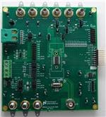
�2.2. Board Assembly
The schematic of the evaluation board can be seen in section 10.
Figure 2 – LMP90100 Evaluation Board Assembly
4
LMP90100 EVB User’s Guide
August 2012
�3.0. Example #1: Quick Start – DC Reading
The following procedures show a quick method to assemble the LMP90100EB and perform a quick DC
voltage reading.
A.
LMP90100 EB Jumper Connections
1. The jumpers for this example application can be seen in Figure 3 and Table 1. Jumpers not
shown can be left unpopulated.
2. The SPIO-4 board is properly setup out of the box (no assembly required).
3. The schematic for the LMP90100EB can be seen section 10.
Figure 3 – Jumper Settings (Default) for the DC Test
Jumpers
JP1: VA_EXT
March 2009
Pin
P1-P2
Purpose
Source VA externally
SNAU028A
5
�JP2: VIO_EXT
JP6
JP7
JP10: VIN_JMP
JP10: VIN_JMP
JP13: VREF_JMP1
JP13: VREF_JMP1
JP14: VREF_JMP2
JP14: VREF_JMP2
P1-P2
P1-P2
P1-P2
P5-P6
P7-P8
P3-P4
P9-P10
P1-P2
P3-P4
Source VIO externally
Connect VA supply to the LMP90100
Connect VIO supply to the LMP90100
Connect a DC input to VIN2
Connect a DC input to VIN3
VREFP1 = 4.1V from U4 (LM4140)
VREFN1 = ground
Connect VREFP1 source to the LMP90100
Connect VREFN1 source to the LMP90100
Table 1 - Jumpers for DC Measurement
B. Installing/Opening the Software - follow section 9.0 to install and open the LMP90100 Sensor
AFE software.
C. Connecting and Powering the Boards – these steps have to be done in this order.
1. Connect a 5.0V power supply to J1 (VA_EXT) and GND (J2). Don’t turn on the power
supply yet.
2. Connect a 5.0V power supply to J3 (VIO_EXT) and GND (J2). Don’t turn on the power
supply yet.
3. Turn on the power supply that is sourcing VA (J1), and then turn on the power supply that is
sourcing VIO (J3).
4. Connect the LMP90100EB’s JP12 to SPIO-4 Board’s J6 (pins 1-16). See Figure 4.
Figure 4 – LMP90100EB-to-SPIO-4 Board Connection
5. Connect SPIO-4 board to a PC via USB.
6. Use a multimeter to measure LMP90100EB’s JP6, JP7; they should all be approximately 5V.
If they are not, check your power supplies and jumpers. Measure JP14.P2; it should be
approximately 4.1V. If it’s not, check your jumpers and U4.
D. Configuring the LMP90100 Using the Sensor AFE Software
6
LMP90100 EVB User’s Guide
August 2012
�Follow the step-by-step instructions under the “HelpBar” mini-tab (left hand side of the GUI) to
configure the LMP90100 for this example. These step-by-step instructions are discussed in
details below, and the recommended configuration should look similar to the figure below.
Figure 5 - Recommended LMP90100 Configuration for a DC Reading
1. Step 1: Select a Sensor - select “DC” “DC” since the input source is not a sensor.
2. Step 2: Configure Inputs – click on the “INPUT MUX” block to set “VINP = 000: VIN2”
and “VINN = 001: VIN3”. Since VIN0 = (3/4) VREF1 and VIN1 = (1/4) VREF1, the
measurement across this channel will be (1/2) VREF1.
3. Step 3: Source IB1/IB2? – this step can be ignored because neither IB1 nor IB2 is connected
to the inputs.
4. Step 4: Select Reference – click on the “VREF MUX” block to choose “VREF_SEL = 0:
VREF1”. Make sure the VREF1 value on the upper left hand side of the GUI is 4.1V
(default).
5. Step 5: Set Gain – since VIN = (1/2) VREF1, the maximum gain that can be set is 2 (with
buffer disabled). If the buffer is enabled, then the output might rail and enable the
“OFLO_FLAGS” flag. In this case, set the gain to 1. Click on the “FGA” block, “PGA”
block, or the “Gain” slider to select the gain.
March 2009
SNAU028A
7
�6. Step 6: Set Buffer – click on the “BUFF” block to include or exclude the buffer from the
signal path.
7. Step 7: Set Calibration - click on the “No Calibration” block to enable or disable calibration.
Refer to the LMP90100 datasheet to more information on the LMP90100’s background
calibration types and modes.
8. Step 8: Int/Ext CLK? – click on the “CLK MUX” block and make sure the internal clock is
selected.
9. Step 9: Performance - click on the “Performance” mini-tab. This tab displays the Estimated
Device Performance base on the block diagram that you’ve configured, as well as the
Measured System Performance if you’ve connected a board and ran the LMP90100.
E. Capturing Data
1. Click on the “Measurement” tab and set the “Scan Mode” as follows:
Figure 6 - Scan Mode Settings
2. Under the “Output Format” field, select Display as “Output Voltage (V)”
3. Under the “Stop Condition” field, select Run as “1000” samples.
4. Click on the “Run” button to view the output voltage results. A reading of approximately
½(VREF1) should be plotted as seen in Figure 7.
8
LMP90100 EVB User’s Guide
August 2012
�Figure 7 - Results for Example #1 - DC Reading
March 2009
SNAU028A
9
�4.0. Example #2: Shorted Input and Calibration Test
This example demonstrates LMP90100’s ability to calibrate for offset error.
A. LMP90100 EB Jumper Connections
1. Connect the LMP90100EB jumpers like the jumpers shown in the figure and table below.
Jumpers not mentioned can be left unconnected.
2. The SPIO-4 board is properly setup out of the box (no assembly required).
3. The schematic for the LMP90100EB can be seen in section 10.
Figure 8 – LMP90100EB Jumper Settings for the Shorted input and Calibration Test
Jumpers
JP1: VA_EXT
JP2: VIO_EXT
JP4
JP6
JP7
JP9
JP10: VIN_JMP
JP13: VREF_JMP1
JP13: VREF_JMP1
10
LMP90100 EVB User’s Guide
Pin
P2-P3
P2-P3
P2-P3
P1-P2
P1-P2
P1-P2
P5-P6
P3-P4
P9-P10
Purpose
Source VA with the 5.0V from the SPIO-4 board.
Source VIO with the 5.0V from the SPIO-4 board.
Get 5.0V from the SPIO-4 board
Connect VA supply to the LMP90100
Connect VIO supply to the LMP90100
Force the odd pins of JP10 to be midscale (VREF1/2)
Connect a DC (midscale) voltage to VIN2
VREFP1 = 4.1V from U4 (LM4140)
VREFN1 = ground
August 2012
�Jumpers
JP14: VREF_JMP2
JP14: VREF_JMP2
Pin
P1-P2
P3-P4
Purpose
Connect VREFP1 source to the LMP90100
Connect VREFN1 source to the LMP90100
Table 2 - Jumpers for the Shorted Input Measurement
B. Installing/Opening the Software – skip this step if it’s already done. If not, follow section 9.0
to install and open the LMP90100 Sensor AFE software.
C. Connecting and Powering the Boards
1. Connect the LMP90100EB to the SPIO-4 board as seen in Figure 4.
2. Connect SPIO-4 board to a PC via USB.
3. Use a multimeter to measure LMP90100EB’s JP6 and JP7; they should all be approximately
5V, and JP14.P2 should be 4.1V. If they are not, check your power supplies and jumpers.
D. Configuring the LMP90100 Using the Sensor AFE Software
Follow the step-by-step instructions under the “HelpBar” mini-tab (left hand side of the GUI) to
configure the LMP90100 for this example. These step-by-step instructions are discussed in
details below, and the recommended configuration should look similar to figure 9.
Figure 9 - Recommended LMP90100 Configuration for the Shorted Input and Calibration Test
1. Step 1: Select a Sensor - select “DC” “DC” since the input source is a DC voltage
March 2009
SNAU028A
11
�2. Step 2: Configure Inputs – click on the “INPUT MUX” block to set “VINP = 000: VIN2”
and “VINN = 000: VIN2”. Since VINP = VINN, a reading of approximately 0V should
be read.
3. Step 3: Source IB1/IB2? – this step can be ignored because neither IB1 nor IB2 is connected
to the inputs.
4. Step 4: Select Reference – click on the “VREF MUX” block to choose “VREF_SEL = 0:
VREF1”. On the left hand side of the GUI, change the VREF1 (left hand side of the GUI)
value to 4.1V.
5. Step 5: Set Gain – since VIN ≈ 0V, the maximum gain that can be set is 128x. Click on the
“FGA” block, “PGA” block, or the “Gain” slider to select the gain.
6. Step 6: Set Buffer – click on the “BUFF” block to include or exclude the buffer from the
signal path.
7. Step 7: Set Calibration - the purpose of this example is to show how the LMP90100 removes
the offset error using background calibration. Initially, disable the calibration by selecting
“000: No Calibration” under the “No Calibration” block.
Refer to the LMP90100 datasheet to more information on the LMP90100’s background
calibration types and modes.
8. Step 8: Int/Ext CLK? – click on the “CLK MUX” block and make sure the internal clock is
selected.
9. Step 9: Performance - click on the “Performance” mini-tab. This tab displays the Estimated
Device Performance base on the block diagram that you’ve configured, as well as the
Measured System Performance if you’ve connected a board and ran the LMP90100.
E. Capturing Data without Calibration
1. Click on the “Measurement” tab and set the “Scan Mode” as follows:
Figure 10 - Scan Mode Settings
2. Under the “Output Format” field, select Display “Output Voltage (V)”
3. Under the “Stop Condition” field, select Run “500” samples.
4. Click on the “Run” button to view the output voltage results. A reading in the hundreds of
uV should be plotted similar to Figure 11.
12
LMP90100 EVB User’s Guide
August 2012
�Figure 11 - Results for Shorted Input Test without Calibration
F. Capturing Data with Calibration
1. In the “Measurement” tab, go to “Quick Control BGCAL_MODE” and change the
background calibration to “001: Offset Cor / Gain Est”.
2. Click on the “Run” button again to view the output voltage results. A mean output reading
closer to 0V should be plotted similar to Figure 12. This decrease in the mean output reading
demonstrates the LMP90100 offset calibration feature.
March 2009
SNAU028A
13
�Figure 12 - Results for Shorted Input Test with Calibration
14
LMP90100 EVB User’s Guide
August 2012
�5.0. Example #3 - 3-wire RTD Application
A 3-wire RTD has a typical configuration shown in Figure 13. This section will explain how to configure
the LMP90100EB and software tool to evaluate a 3-wire RTD.
z
Figure 13 - 3-Wire RTD Configuration
A. LMP90100EB Jumper Connections
1. The jumper settings for this application are shown below. The jumpers not mentioned can be
left unconnected.
2. The SPIO-4 board is properly setup out of the box (no assembly required).
3. The schematic for the LMP90100EB can be seen in section 10.
March 2009
SNAU028A
15
�Figure 14 – Jumper Settings (Default) for the 3-wire RTD Example
Jumpers
JP1: VA_EXT
JP2: VIO_EXT
JP4
JP6
JP7
JP11: RTD_JMP
JP11: RTD_JMP
JP11: RTD_JMP
JP11: RTD_JMP
JP11: RTD_JMP
JP11: RTD_JMP
Pin
P2-P3
P2-P3
P2-P3
P1-P2
P1-P2
P1-P2
P3-P4
P7-P8
P9-P10
P11-P12
P13-P14
Purpose
Source VA with the 5.0V from the SPIO-4 board.
Source VIO with the 5.0V from the SPIO-4 board.
Get 5.0V from the SPIO-4 board
Connect VA supply to the LMP90100
Connect VIO supply to the LMP90100
Connect IB1 to the RTD
Connect the RTD to VIN0
Connect IB2 to the RTD
Connect the RTD to VIN1
Connect the RTD to VREFP2
Connect VREFN2 to ground
Table 3 – LMP90100EB Jumpers for the RTD Application
16
LMP90100 EVB User’s Guide
August 2012
�B. Installing/Opening the Software – skip this step if it’s already done. If not, follow section 9.0
to install and open the LMP90100 Sensor AFE software.
C. Connecting and Powering the Boards
1. Connect the LMP90100EB to the SPIO-4 board as seen in Figure 4.
2. Connect SPIO-4 board to a PC via USB.
3. Use a multimeter to measure LMP90100EB’s JP6 and JP7; they should all be approximately
5.0V. If they are not, check your power supplies and jumpers.
D. Connecting the Sensor to the LMP90100EB
1. Connect a 3-wire RTD to J10 as seen in the image below. The white wire should be at
J10.P1, and the red wires should be at J10.P3 and J10.P4.
Figure 15 – Jumper Settings (Default) for the 3-wire RTD Example
E. Configuring the LMP90100 Using the Sensor AFE Software
Follow the step-by-step instructions under the “HelpBar” mini-tab (left hand side of the GUI) to
configure the LMP90100 for this example. These step-by-step instructions are discussed in
details below, and the recommended configuration should look similar to Figure 16.
March 2009
SNAU028A
17
�Figure 16 - Recommended LMP90100 Configuration for a PT-100 RTD
1. Step 1: Select a Sensor - select “RTD” “PRTF-10-2-100-1/4-6-E”.
2. Step 2: Configure Inputs – click on the “INPUT MUX” block to set “VINP = 000: VIN0”
and “VINN = 001: VIN1”. Click on the “Eval. Board Settings” button located next to
the block diagram. This should open up a PDF of the schematic and calculation for this 3wire RTD example.
3. Step 3: Source IB1/IB2? – click on the “EXC. Current” block to set “RTD_CUR_SEL =
1010: 1000 uA”.
4. Step 4: Select Reference – click on the “VREF MUX” block to choose
“VREF_SEL = 1: VREF2”. Make sure the value for VREF2 (upper left hand side of the
GUI) is 2.0V = [RREF * (IB1+IB2)] = [1k * (1mA + 1mA)].
5. Step 5: Set Gain – since VIN = 0.109 V at room temperature for IB1 = IB2 = 1000 uA, the
maximum gain can be 16x. Click on the “FGA” block, “PGA” block, or the “Gain” slider
to select the gain. (For this exercise, the gain can be set to 1x).
6. Step 6: Set Buffer – click on the “BUFF” block to include or exclude the buffer from the
signal path. (For this exercise, the buffer can be disabled).
18
LMP90100 EVB User’s Guide
August 2012
�7. Step 7: Set Calibration - click on the “No Calibration” block to enable or disable calibration.
Refer to the LMP90100 datasheet to more information on the LMP90100’s background
calibration types and modes. (For this exercise, the calibration can be OFF).
8. Step 8: Int/Ext CLK? – click on the “CLK MUX” block and make sure the internal clock is
selected.
9. Step 9: Performance - click on the “Performance” mini-tab. This tab displays the Estimated
Device Performance base on the block diagram that you’ve configured, as well as the
Measured System Performance if you’ve connected a board and ran the LMP90100.
F. Capturing Data
1. Click on the “Measurement” tab and set the “Scan Mode” as follows:
Figure 17 - Scan Mode Settings
2. Under the “Output Format” field, select Display “Temperature (°C)”
3. Make sure the “Sensor Characteristics” is set as:
4. Under the “Stop Condition” field, select “Run Continuously”.
5. Click on the “Run” button to view the output temperature reading. A reading of
approximately 23°C to 25°C (room temperature) should be plotted.
March 2009
SNAU028A
19
�Figure 18 – Reading of Room Temperature Using the 3-Wire RTD
20
LMP90100 EVB User’s Guide
August 2012
�6.0. Example #4: Thermocouple and LM94022 Application
A. Thermocouple and Cold Junction Compensation Background
Figure 19 – Thermocouple and Temperature Sensor Connection
As described in section 17.6.2. of the LMP90100 datasheet, because a thermocouple can only
measure a voltage difference and thus a temperature difference (relative temperature), it does not
have the ability to measure absolute temperature. To determine the absolute temperature of the
measured environment, a technique known as cold junction compensation (CJC) must be used.
In a CJC technique, the “cold” junction temperature, Tcold (Figure 19), is sensed by using an IC
temperature sensor, such as the LM94022. The temperature sensor should be placed within close
proximity of the reference junction. The LM94022 is placed underneath the thermocouple
connector J4 on the LMP90100 evaluation board.
The technique to calculate for Thot using the CJC method can be found in the LMP90100
datasheet.
The Sensor AFE software does have the ability to display the relative thermocouple temperature
using a Type K look-up-table (http://www.intech.co.nz/products/temperature/typek.html). In
addition, if the LM94022 (or any other temperature sensors) is connected to the LMP90100, then
the software can also read its temperature (Tcold). However, the user has to manually enter this
Tcold value in the
field located on the upper
left hand side of the GUI. The software will use this T_board value to calculate for Thot.
B. Thermocouple and LM94022 Schematic on the LMP90100EB
March 2009
SNAU028A
21
�The thermocouple and temperature sensor schematic of the LMP90100 Evaluation Board are
shown below. The temperature sensor is a LM94022 and is located under the thermocouple
connector (J4) to provide cold junction compensation. The thermocouple connector (J4) is made
for use with a type K thermocouple. The following subsections will explain how to configure the
LMP90100EB for the thermocouple and IC temperature sensor applications.
Figure 20 – Thermocouple and Temperature Sensor Schematic
C. LMP90100EB Jumper Connections:
1. The figure and table below show the LMP90100 evaluation board jumper settings for this
thermocouple application. The jumpers not mentioned can be left unconnected.
2. The SPIO-4 board is properly setup out of the box (no assembly required).
3. The schematic for the LMP90100EB can be seen in section 10.
22
LMP90100 EVB User’s Guide
August 2012
�Figure 21 – Jumper Settings for the Thermocouple and LM94022 Example
Jumpers
JP1: VA_EXT
JP2: VIO_EXT
JP4
JP6
JP7
JP5: TC_JMP
JP5: TC_JMP
JP3: LM94022_JMP
JP13: VREF_JMP1
JP13: VREF_JMP1
JP14: VREF_JMP2
JP14: VREF_JMP2
Pin
P2-P3
P2-P3
P2-P3
P1-P2
P1-P2
P1-P2
P3-P4
P1-P2
P3-P4
P9-P10
P1-P2
P3-P4
Purpose
Source VA with the 5.0V from the SPIO-4 board.
Source VIO with the 5.0V from the SPIO-4 board.
Get 5.0V from the SPIO-4 board
Connect VA supply to the LMP90100
Connect VIO supply to the LMP90100
Connect TCN to VIN3
Connect TCP to VIN4
Connect the output of LM94022 to VIN5
VREFP1 = 4.1V from U4 (LM4140)
VREFN1 = ground
Connect VREFP1 source to the LMP90100
Connect VREFN1 source to the LMP90100
Table 4 – LMP90100EB Jumpers for the RTD Application
D. Installing/Opening the Software – skip this step if it’s already done. If not, follow section 9.0
to install and open the LMP90100 Sensor AFE software.
E. Connecting and Powering the Boards
1. Connect the LMP90100EB to the SPIO-4 board as seen in Figure 4.
March 2009
SNAU028A
23
�2. Connect SPIO-4 board to a PC via USB.
3. Use a multimeter to measure LMP90100EB’s JP6, JP7, and JP14.P2; they should all be
approximately 5V. If they are not, check your power supplies and jumpers.
F. Connect a K type thermocouple to J4. Note that the thermocouple’s positive input
(TCP) = VIN4 and negative input (TCN) = VIN3.
G. Configuring the LMP90100 for the LM94022 Using the Sensor AFE Software
Follow the step-by-step instructions under the “HelpBar” mini-tab (left hand side of the GUI) to
configure the LMP90100 for the LM94022 IC sensor. These step-by-step instructions are
discussed in details below, and the recommended configuration should look similar to Figure 22.
Figure 22 - Recommended LMP90100 Configuration for the LM94022
1. Step 1: Select a Sensor – click on the “+” button to enter the “Sensor Database” tab. Select
“Analog” “LM94022”.
2. Step 2: Configure Inputs – click on the “INPUT MUX” block to set “VINP = 101: VIN5”
and “VINN = 111: VIN7”. Click on the “Eval. Board Settings button located next to
the block diagram. This should open up a PDF of the schematic of the thermocouple and
LM94022 application.
3. Step 3: Source IB1/IB2? – this step can be ignored because neither IB1 nor IB2 is connected
to the inputs.
24
LMP90100 EVB User’s Guide
August 2012
�4. Step 4: Select Reference – click on the “VREF MUX” block to choose “VREF_SEL = 0:
VREF1”. Make sure the value for VREF1 = 4.1V.
5. Step 5: Set Gain – click on the “FGA” block, “PGA” block, or the “Gain” slider to select
the gain. The gain can be set to 1 in this example.
6. Step 6: Set Buffer – click on the “BUFF” block to include or exclude the buffer from the
signal path. The buffer can be excluded from the signal path in this example.
7. Step 7: Set Calibration - click on the “No Calibration” block to enable or disable calibration.
Refer to the LMP90100 datasheet to more information on the LMP90100’s background
calibration types and modes. The calibration can be OFF for this example.
8. Step 8: Int/Ext CLK? – click on the “CLK MUX” block and make sure the internal clock is
selected.
9. Step 9: Performance - click on the “Performance” mini-tab. This tab displays the Estimated
Device Performance base on the block diagram that you’ve configured, as well as the
Measured System Performance if you’ve connected a board and ran the LMP90100.
H. Configuring the LMP90100 for the Thermocouple Using the Sensor AFE Software
Follow the step-by-step instructions under the “HelpBar” mini-tab (left hand side of the GUI) to
configure the LMP90100 for the thermocouple. These step-by-step instructions are discussed in
details below, and the recommended configuration should look similar to the figure below.
March 2009
SNAU028A
25
�Figure 23 - Recommended LMP90100 Configuration for a Thermocouple
1. Step 1: Select a Sensor - select “Thermocouple” select the thermocouple of your choice
or add your own thermocouple by clicking on “New”.
2. Step 2: Configure Inputs – click on the “INPUT MUX” block to set “VINP = 100: VIN4”
and “VINN = 011: VIN3”. Click on the “Eval. Board Settings button located next to the
block diagram. This should open up a PDF of the schematic for a thermocouple.
3. Step 3: Source IB1/IB2? – this step can be ignored because neither IB1 nor IB2 is connected
to the inputs.
4. Step 4: Select Reference – click on the “VREF MUX” block to choose “VREF_SEL = 0:
VREF1”. Make sure the value for VREF1 = 4.1V.
5. Step 5: Set Gain – since the differential junction across a thermocouple is low, the maximum
gain can be 128x. Click on the “FGA” block, “PGA” block, or the “Gain” slider to select
the gain. In this example, the gain can be 1x.
6. Step 6: Set Buffer – click on the “BUFF” block to include or exclude the buffer from the
signal path. The buffer can be excluded from the signal path in this example.
7. Step 7: Set Calibration - click on the “No Calibration” block to enable or disable calibration.
Refer to the LMP90100 datasheet to more information on the LMP90100’s background
calibration types and modes. In this example, the calibration can be OFF.
26
LMP90100 EVB User’s Guide
August 2012
�8. Step 8: Int/Ext CLK? – click on the “CLK MUX” block and make sure the internal clock is
selected.
9. Step 9: Performance - click on the “Performance” mini-tab. This tab displays the Estimated
Device Performance base on the block diagram that you’ve configured, as well as the
Measured System Performance if you’ve connected a board and ran the LMP90100.
F. Capturing Data
1. Click on the “Measurement” tab and set the “Scan Mode” as follows:
Figure 24 - Scan Mode Settings
2.
3.
4.
5.
March 2009
Under the “Output Format” field, select Display “Temperature (C)”
Under the “Run For” field, plot the “Selected Channel: CH0”
Under the “Stop Condition” field, select Run “1000 Samples”.
Click on the “Run” button to capture the temperature (Tcold) reading from the LM94022
(see figure below).
SNAU028A
27
�Figure 25 – Temperature Sensor Reading for Tcold
6. Enter the LM94022’s mean temperature (see red box in the figure above) in the
“T_board” field located on the upper left hand side of the GUI. The software will use
this “T_board” value to calculate for the thermocouple’s absolute temperature (Thot).
If the LM94022 or any other temperature sensor is not connected to do cold junction
compensation, then the user can still manually enter a Tcold value in the “T_board” field
box.
7. In the Sensor Window, click on CH1 to read the thermocouple’s voltage and temperature.
Figure 26 – Sensor Window
8. In the “Measurement” tab, choose the “Output Format” as “Output Voltage (V)”,
and click “Run” to capture the thermocouple relative voltage.
Figure 27 – Thermocouple Voltage Relative Reading
28
LMP90100 EVB User’s Guide
August 2012
�9. In the “Output Format” field, choose to Display “Rel. Temp (C)”. This shows the
relative temperature of the thermocouple. This reading is not factoring in the cold
junction compensation.
Figure 28 – Thermocouple Relative Temperature Reading
10. In the “Output Format” field, choose to Display “Abs. Temp (C)”. This uses the
“T_board” temperature and factor in the cold junction compensation method to display
the absolute temperature (Thot) of the thermocouple.
March 2009
SNAU028A
29
�Figure 29 – Thermocouple Absolute Temperature Reading
30
LMP90100 EVB User’s Guide
August 2012
�7.0. Powering the LMP90100EB
There are two ways in which VA and VIO can be sourced: external supplies or SPIO-4 power.
If using external power supplies to source VA and VIO, then do the following:
1. Connect an external power supply to J1 for VA. Jumper pins 1 and 2 of JP1 to select this option.
2. Connect an external power supply to J2 for VIO. Jumper pins 1 and 2 of JP2 to select this option.
3. Jumper JP6 to connect the external power to VA.
4. Jumper JP7 to connect the external power to VIO.
If using the SPIO-4 power to source VA and VIO, then do the following:
1. Jumper pins 1 and 2 of JP4 to select 3.3V for VA and VIO, or jumper pins 2 and 3 of JP4 to
select 5.0V for VA and VIO.
2. Jumper pins 2 and 3 of JP1 to select the SPIO-4 power for VA.
3. Jumper pins 2 and 3 of JP2 to select the SPIO-4 power for VIO.
4. Jumper JP6 to connect the SPIO-4 power to VA.
5. Jumper JP7 to connect the SPIO-4 power to VIO.
The schematic for the LMP90100EB can be seen in section 10.
8.0. Evaluating the LMP90100 without the SPIO-4 Board.
The SPIO-4 digital controller board is used to generate the SPI signals to communicate to the
LMP90100. Without the SPIO-4 board, the Sensor AFE software for the LMP90100 cannot be used
to capture and analyze data from the LMP90100EB.
If the SPIO-4 board is not available but LMP90100 evaluation is desirable, then connect your own
SPI signals to J8 of the LMP90100EB as seen below.
Figure 30 - LMP90100EB’s J8 for SPI Signals
Refer to the LMP90100 datasheet for more information on the LMP90100’s SPI protocol.
March 2009
SNAU028A
31
�9.0. Installing the LMP90100 Sensor AFE Software
Each Sensor AFE product will have its own software. To access the Sensor AFE software for
LMP90100, follow the steps below.
1. Getting the Zip Files
a. You can find the latest downloadable Sensor AFE software at www.ti.com/sensorafe
Tools
b. Download the zip file onto your local hardrive. Unzip this folder.
2. Installing the Driver - skip this step if you don’t have the LMP90100EB and SPIO4 digital
controller board.
a. Connect the LMP9100EB to SPIO4 board
b. Connect the SPIO4 board to your PC.
c. Follow the steps below to install the driver:
Figure 31 - Click on "No, not this time"
32
LMP90100 EVB User’s Guide
August 2012
�Figure 32 – Choose to “install from a list or specific location (Advanced)”
Figure 33 – Find the driver in the “NSC_USB_v1.0.8.0” folder
(it should be located in the unzipped folder)
March 2009
SNAU028A
33
�Figure 34 – Waiting for the computer to install the driver
34
LMP90100 EVB User’s Guide
August 2012
�Figure 35 – Installation is complete
3. Open the un-zipped folder and click on “lmp90100.exe” to start the software. If you don’t have
the boards, you’ll get an error message. Ignore that error message and click “Ok” to continue.
March 2009
SNAU028A
35
�10.0. Schematic
OUT
VDD
4
2
GND
R2
2k, 0.1%
TCN
C3
10nF
C4
2.2uF
2
4
1
3
3
1
2
2
3
1
1
1
VIO
R6
1M
VIO
R10
1M
VIO
R11
1M
VIO
R12
1M
VIO
R13
1M
VIO
R14
1M
VIO
R15
1M
VIO
TP6
GND
JP8
GPIO_2_GND
R16
1M
GND
51
D6_DRDY B2
R18
D5
D4
D3
D2
D1
D0
SDO_DRDY B 51
R20
SDI
SCLK
CSB
GND
XIN_CLK
GND
GND
1
CSB
3
SCLK
SDO_DRDY B2 5
7
SDI
9
11
SDA
13
VDD3P3
15
VIO
1
TP15
GND
RREF
1k, 0.1%
GND
1
2
1
1
GND
VREFN1
GND
L4
100 uH
1
C21
0.1 uF
VIN7_VREFN2
GND
C29
0.1 uF
1
SCL
VDD5P0
GND
C19
0.1 uF
GND
SCL
SDA
GND
TP16
GND
1
VIN6_VREFP2
C27
10 uF
D6_DRDY B2 GND
C28
10 uF
1
C20
0.1 uF
1 2
VREFP1
VREFP1
VREFN1
VIN6_VREFP2
VIN7_VREFN2
2
2
4
6
8
1
1
3
5
7
GND
VDD3P3
GND
1
C26
10nF
2
1
C25
NS
2
L3
100 uH
2
4
6
8
10
2
J13
VREFN_EXT
1
1
3
5
7
9
VA
4P1V
GND
GND
2
4
6
8
10
12
14
16
U3
24C02 EEPROM
8
VCC
A0
7
2
WP
A1
6
3
SCL
A2
5
4
GND SDA
C18
0.1 uF
GND
1
1.0 uF
C24
GND
2
J12
GND
J11
VREFP_EXT
1
1
TP17
GND
GND
2
C23
0.1 uF
JP14
VREF_SELECT2
1
GND
JP13
VREF_SELECT1
1
1
2
GND
2
4
6
8
10
12
14
16
1
GND
GND
2
1
2
C22
1.0 uF
U4
LM4140C-4.1 (NS)
8
GND GND3 7
VIN GND2 6
EN VREF 5
GND1 NC
1
3
5
7
9
11
13
15
VDD3P3
GND
1
2
3
4
TP13
GND
JP12
SPIO4 CONNECTOR
GND
GND
GND
VDD5P0
GND
TP12
GND
1
GND
TP14
GND
1
IB1
VIN0
VIN2
IB2
VIN1
VIN6_VREFP2
VIN7_VREFN2
1
RRTD2 0
2
4
6
8
10
12
14
TP11
GND
1
TP10
GND
TP9
GND
J8
SPI_PROBE
1
5
1
1
1
NS
R25
51
1
1
3
5
7
9
11
13
RRTD1 0
1
2
3
4
5
SDO_DRDYB
SDI
SCLK
CSB
GND
GND
10nF
2
1
R19
1k, 0.1%
SDO_DRDY B2
EXT_CLK
J9
R24
2
4
6
8
10
12
14
1
3
5
7
9
11
13
2
C16
12pF
VIO
R9
1M
1
D6_DRDY B
R23
0
2
1
JP11
RTD_SELECT
2
C15
12pF
VIO
R8
1M
1
Y1
3.57 MHz
R22
0
28
27
26
25
24
23
22
21
20
19
18
17
16
15
R7
1M
1
2
GND
VIO
VA
D6_DRDY B
VIN0
D5
VIN1
D4
VIN2
D3
VIN3
D2
VIN4
D1
VIN5
D0
VREFP1
SDO_DRDY B
VREFN1
SDI
VIN6_VREFP2
SCLK
VIN7_VREFN2
CSB
IB2
GND
IB1
XIN_CLK
XOUT
VIO
1
C11
0.1 uF
GND
2
3
4
1
2
VIN0
3
VIN1
4
VIN2
5
VIN3
6
VIN4
7
VIN5
8
VREFP1
9
VREFN1
VIN6_VREFP2 10
11
VIN7_VREFN2
12
IB2
13
IB1
14
XOUT
GND
C14
2.2uF
C17
GND
1
GND
1
U2
LMP90100
GND
1
GND
GND
1
2
3
4
C10
1.0 uF
2
C9
NS
C8
0.1 uF
2
2
1
1
C7
1.0 uF
GND GND
1
TP7
GND
1
1
1
1
2
C13
10 uF
2
1
2
4
6
8
10
12
14
16
1
3
5
7
9
11
13
15
1
JP9
VIN_SHORT
1
2
1
1
JP10
INPUT_SELECT
GND
C12
2.2uF
R21
1k, 0.1%
1
GND
1
C6
NS
1
J7
VIN1
2
J6
GND
J5
VIN0
J10
RTD
1
2
GND
VREFP1
R5
1k, 0.1%
JP7
VIO_JMP
2
1
GND
GND
TP5
GND
1
1
JP6
VA_JMP
1
C5
10nF
1
TP4
GND
2
R4
2k, 0.1%
VIO
VA
TCP
GND
1
1
VIN3
VIN4
2
1
1
VREFP1
R3
2k, 0.1%
R17
2k, 0.1%
VDD5P0
JP4
SPIO4_PWR_SELECT
VIO
JP5
TC_SEL
2
1
2
GND
TP8
GND
GND
1
1
1
TC-
GND
GND
VA
L2
100 uH
R1
2k, 0.1%
J4
THERMOCOUPLE
TC+
L1
100 uH
C2
0.1 uF
2
Place LM94022 underneath thermocouple's connector
(not underneath the board)
GND
SPIO4_PWR
VDD3P3
VDD5P0
C1
1.0 uF
LM94022_JMP
VIO_SELECT
JP2
J3
VIO_EXT
1
TP2
GND
2
1
1
GND
JP3
TP3
GND
J2
GND
SPIO4_PWR
GND
1
3
VA_SELECT
JP1
J1
VA_EXT
1
TP1
GND
5
1
GND
2
1
VIN5
GS1
GS0
1
2
3
U1
LM94022BIMG
1
GND
C30
0.1 uF
GND
GND
Title
LMP90100 Customer Ev aluation Board
Size
C
Date:
Figure 36 - LMP90100EB Schematic
36
LMP90100 EVB User’s Guide
August 2012
Document Number
600496
Wednesday , Nov ember 23, 2011 Sheet
Rev
18
1
of
1
�11.0. Layout
Figure 37 - Layout – Top Layer
March 2009
SNAU028A
37
�Figure 38 - Layout 3rd Layer
38
LMP90100 EVB User’s Guide
August 2012
�12.0. BOM
Item
1
2
Value
1.0 uF
0.1 uF
Description
CAP CER 1.0UF 10V Y5V 0603
CAP CER .1UF 0603
Source
Digikey
Digikey
Source Part #
490-1585-1-ND
490-4779-1-ND
3
4
6
7
9
10
11
12
13
14
15
16
17
18
19
20
21
22
Quantity Reference
5
C1,C7,C10,C22,C24
10
C2,C8,C11,C18,C19,C20,
C21,C23,C29,C30
4
C3,C5,C17,C26
3
C4,C12,C14
3
C13,C27,C28
2
C15,C16
1
JP1
1
JP2
1
JP3
1
JP4
1
JP5
1
JP6
1
JP7
1
JP8
1
JP9
1
JP10
1
JP11
1
JP12
1
JP13
1
JP14
10nF
2.2uF
10 uF
12pF
VA_SELECT
VIO_SELECT
LM94022_JMP
SPIO4_PWR_SELECT
TC_SEL
VA_JMP
VIO_JMP
GPIO_2_GND
VIN_SHORT
INPUT_SELECT
RTD_SELECT
SPIO4 CONNECTOR
VREF_SELECT1
VREF_SELECT2
Digikey
Digikey
Digikey
Digikey
Digikey
Digikey
Digikey
Digikey
Digikey
Digikey
Digikey
Digikey
Digikey
Digikey
Sullins Connector
Digikey
Digikey
Digikey
490-1512-1-ND
490-1743-1-ND
445-1371-1-ND
PCC120CNCT-ND
S1011E-36-ND
S1011E-36-ND
S1011E-36-ND
S1011E-36-ND
S1011E-36-ND
S1011E-36-ND
S1011E-36-ND
S1011E-36-ND
S1011E-36-ND
S1011E-36-ND
S1011E-36-ND
A34278-40-ND
S1011E-36-ND
S1011E-36-ND
23
1
J1
VA_EXT
Digikey
J147-ND
24
3
J2,J6,J12
GND
Digikey
J147-ND
25
26
1
1
J3
J4
VIO_EXT
THERMOCOUPLE
Digikey
RS Mobile
J147-ND
381-7564
27
1
J5
VIN0
CAP CER 10000PF 50V 10% X7R 0603
CAP CER 2.2UF 10V Y5V 0805
CAP CER 10UF 10V Y5V 0805
CAP 12PF 50V CERM CHIP 0805 SMD
CONN HEADER .100 SINGL STR 36POS
CONN HEADER .100 SINGL STR 36POS
CONN HEADER .100 SINGL STR 36POS
CONN HEADER .100 SINGL STR 36POS
CONN HEADER .100 SINGL STR 36POS
CONN HEADER .100 SINGL STR 36POS
CONN HEADER .100 SINGL STR 36POS
CONN HEADER .100 SINGL STR 36POS
CONN HEADER .100 SINGL STR 36POS
CONN HEADER .100 SINGL STR 36POS
CONN HEADER .100 SINGL STR 36POS
CONN HEADR BRKWAY .100 80POS R/A
CONN HEADER .100 SINGL STR 36POS
CONN HEADER .100 SINGL STR 36POS
CONN JACK BANANA UNINS PANEL
MOU
CONN JACK BANANA UNINS PANEL
MOU
CONN JACK BANANA UNINS PANEL
MOU
THERMOCOUPLE CLASS K SOCKET
CONN JACK BANANA UNINS PANEL
MOU
Digikey
J147-ND
March 2009
SNAU028A
39
�28
29
30
31
1
1
1
1
J7
J8
J9
J10
VIN1
SPI_PROBE
EXT_CLK
RTD
32
1
J11
VREFP_EXT
33
34
1
4
J13
L1,L2,L3,L4
VREFN_EXT
100 uH
CONN JACK BANANA UNINS PANEL
MOU
CONN HEADER .100 SINGL STR 36POS
CONN BNC FEM JACK PC MNT STRGHT
TERM BLOCK PCB 4POS 5.0MM GREEN
CONN JACK BANANA UNINS PANEL
MOU
CONN JACK BANANA UNINS PANEL
MOU
INDUCTOR 100UH 140MA 10% SMD
35
4
R5,R19,R21,RREF
1k, 0.1%
RES 1.0K OHM 1/8W .1% 0805 SMD
Digikey
36
37
4
5
RRTD1,RRTD2,R22,R23
R1,R2,R3,R4,R17
0
2k, 0.1%
RES 0.0 OHM 1/10W 0603 SMD
RES 2.0K OHM 1/8W .1% 0805 SMD
Digikey
Digikey
38
11
1M
RES 1.0M OHM 1/8W 5% 0805 SMD
39
41
3
17
51
GND
42
43
44
45
46
47
1
1
1
1
1
4
R6,R7,R8,R9,R10,R11,R12,
R13,R14,R15,R16
R18,R20,R25
TP1,TP2,TP3,TP4,TP5,TP6,
TP7,TP8,TP9,TP10,TP11,
TP12,TP13,TP14,TP15,TP16,
TP17
U1
U2
U3
U4
Y1
N/A
LM94022BIMG
LMP90100
24C02 EEPROM
LM4140C-4.1
3.57 MHz
N/A
Digikey
Digikey
Digikey
Digikey
J147-ND
S1011E-36-ND
ACX1051-ND
277-1579-ND
Digikey
J147-ND
Digikey
Digikey
Digikey
J147-ND
587-2038-1-ND
RG20P1.0KBCTND
RMCF1/160RCTND
P2.0KDACT-ND
RHM1.0MARCTND
RES 51 OHM 1/10W 5% 0603 SMD
TEST POINT PC MULTI PURPOSE BLK
Digikey
Digikey
P51GCT-ND
5011K-ND
ANALOG TEMPERATURE SENSOR
LMP90100
EEPROM 256x8
4.1 V Voltage Reference
CRYSTAL 3.579545 MHZ 18PF 49US
BUMPON HEMISPHERE .44X.20 BLACK
NSC
NSC
Mouser
NSC
Digikey
Digikey
LM94022BIMG
LMP90100
579-24C02CSN
LM4140C-4.1
XC1707-ND
SJ5003-0-ND
Table 5 - BOM
40
LMP90100 EVB User’s Guide
August 2012
��EVALUATION BOARD/KIT/MODULE (EVM) ADDITIONAL TERMS
Texas Instruments (TI) provides the enclosed Evaluation Board/Kit/Module (EVM) under the following conditions:
The user assumes all responsibility and liability for proper and safe handling of the goods. Further, the user
indemnifies TI from all claims arising from the handling or use of the goods.
Should this evaluation board/kit not meet the specifications indicated in the User’s Guide, the board/kit may be
returned within 30 days from the date of delivery for a full refund. THE FOREGOING LIMITED WARRANTY IS THE
EXCLUSIVE WARRANTY MADE BY SELLER TO BUYER AND IS IN LIEU OF ALL OTHER WARRANTIES,
EXPRESSED, IMPLIED, OR STATUTORY, INCLUDING ANY WARRANTY OF MERCHANTABILITY OR FITNESS
FOR ANY PARTICULAR PURPOSE. EXCEPT TO THE EXTENT OF THE INDEMNITY SET FORTH ABOVE,
NEITHER PARTY SHALL BE LIABLE TO THE OTHER FOR ANY INDIRECT, SPECIAL, INCIDENTAL, OR
CONSEQUENTIAL DAMAGES.
Please read the User's Guide and, specifically, the Warnings and Restrictions notice in the User's Guide prior to
handling the product. This notice contains important safety information about temperatures and voltages. For
additional information on TI's environmental and/or safety programs, please visit www.ti.com/esh or contact TI.
No license is granted under any patent right or other intellectual property right of TI covering or relating to any
machine, process, or combination in which such TI products or services might be or are used. TI currently deals
with a variety of customers for products, and therefore our arrangement with the user is not exclusive. TI assumes
no liability for applications assistance, customer product design, software performance, or infringement of patents
or services described herein.
REGULATORY COMPLIANCE INFORMATION
As noted in the EVM User’s Guide and/or EVM itself, this EVM and/or accompanying hardware may or may not be
subject to the Federal Communications Commission (FCC) and Industry Canada (IC) rules.
For EVMs not subject to the above rules, this evaluation board/kit/module is intended for use for ENGINEERING
DEVELOPMENT, DEMONSTRATION OR EVALUATION PURPOSES ONLY and is not considered by TI to be a
finished end product fit for general consumer use. It generates, uses, and can radiate radio frequency energy and
has not been tested for compliance with the limits of computing devices pursuant to part 15 of FCC or ICES-003
rules, which are designed to provide reasonable protection against radio frequency interference. Operation of the
equipment may cause interference with radio communications, in which case the user at his own expense will be
required to take whatever measures may be required to correct this interference.
General Statement for EVMs including a radio
User Power/Frequency Use Obligations: This radio is intended for development/professional use only in legally
allocated frequency and power limits. Any use of radio frequencies and/or power availability of this EVM and its
development application(s) must comply with local laws governing radio spectrum allocation and power limits for
this evaluation module. It is the user’s sole responsibility to only operate this radio in legally acceptable frequency
space and within legally mandated power limitations. Any exceptions to this are strictly prohibited and unauthorized
by Texas Instruments unless user has obtained appropriate experimental/development licenses from local
regulatory authorities, which is responsibility of user including its acceptable authorization.
For EVMs annotated as FCC – FEDERAL COMMUNICATIONS COMMISSION Part 15 Compliant
Caution
This device complies with part 15 of the FCC Rules. Operation is subject to the following two conditions: (1) This
device may not cause harmful interference, and (2) this device must accept any interference received, including
interference that may cause undesired operation.
Changes or modifications not expressly approved by the party responsible for compliance could void the user's
authority to operate the equipment.
FCC Interference Statement for Class A EVM devices
�This equipment has been tested and found to comply with the limits for a Class A digital device, pursuant to part 15
of the FCC Rules. These limits are designed to provide reasonable protection against harmful interference when
the equipment is operated in a commercial environment. This equipment generates, uses, and can radiate radio
frequency energy and, if not installed and used in accordance with the instruction manual, may cause harmful
interference to radio communications. Operation of this equipment in a residential area is likely to cause harmful
interference in which case the user will be required to correct the interference at his own expense.
FCC Interference Statement for Class B EVM devices
This equipment has been tested and found to comply with the limits for a Class B digital device, pursuant to part 15
of the FCC Rules. These limits are designed to provide reasonable protection against harmful interference in a
residential installation. This equipment generates, uses and can radiate radio frequency energy and, if not installed
and used in accordance with the instructions, may cause harmful interference to radio communications. However,
there is no guarantee that interference will not occur in a particular installation. If this equipment does cause
harmful interference to radio or television reception, which can be determined by turning the equipment off and on,
the user is encouraged to try to correct the interference by one or more of the following measures:
•
•
•
•
Reorient or relocate the receiving antenna.
Increase the separation between the equipment and receiver.
Connect the equipment into an outlet on a circuit different from that to which the receiver is connected.
Consult the dealer or an experienced radio/TV technician for help.
For EVMs annotated as IC – INDUSTRY CANADA Compliant
This Class A or B digital apparatus complies with Canadian ICES-003.
Changes or modifications not expressly approved by the party responsible for compliance could void the user’s
authority to operate the equipment.
Concerning EVMs including radio transmitters
This device complies with Industry Canada licence-exempt RSS standard(s). Operation is subject to the following
two conditions: (1) this device may not cause interference, and (2) this device must accept any interference,
including interference that may cause undesired operation of the device.
Concerning EVMs including detachable antennas
Under Industry Canada regulations, this radio transmitter may only operate using an antenna of a type and
maximum (or lesser) gain approved for the transmitter by Industry Canada. To reduce potential radio interference to
other users, the antenna type and its gain should be so chosen that the equivalent isotropically radiated power
(e.i.r.p.) is not more than that necessary for successful communication.
This radio transmitter has been approved by Industry Canada to operate with the antenna types listed in the user
guide with the maximum permissible gain and required antenna impedance for each antenna type indicated.
Antenna types not included in this list, having a gain greater than the maximum gain indicated for that type, are
strictly prohibited for use with this device.
Cet appareil numérique de la classe A ou B est conforme à la norme NMB-003 du Canada.
Les changements ou les modifications pas expressément approuvés par la partie responsable de la conformité ont
pu vider l’autorité de l'utilisateur pour actionner l'équipement.
Concernant les EVMs avec appareils radio
Le présent appareil est conforme aux CNR d'Industrie Canada applicables aux appareils radio exempts de licence.
L'exploitation est autorisée aux deux conditions suivantes : (1) l'appareil ne doit pas produire de brouillage, et (2)
l'utilisateur de l'appareil doit accepter tout brouillage radioélectrique subi, même si le brouillage est susceptible d'en
compromettre le fonctionnement.
Concernant les EVMs avec antennes détachables
Conformément à la réglementation d'Industrie Canada, le présent émetteur radio peut fonctionner avec une
antenne d'un type et d'un gain maximal (ou inférieur) approuvé pour l'émetteur par Industrie Canada. Dans le but
�de réduire les risques de brouillage radioélectrique à l'intention des autres utilisateurs, il faut choisir le type
d'antenne et son gain de sorte que la puissance isotrope rayonnée équivalente (p.i.r.e.) ne dépasse pas l'intensité
nécessaire à l'établissement d'une communication satisfaisante.
Le présent émetteur radio a été approuvé par Industrie Canada pour fonctionner avec les types d'antenne
énumérés dans le manuel d’usage et ayant un gain admissible maximal et l'impédance requise pour chaque type
d'antenne. Les types d'antenne non inclus dans cette liste, ou dont le gain est supérieur au gain maximal indiqué,
sont strictement interdits pour l'exploitation de l'émetteur.
SPACER
SPACER
SPACER
【Important Notice for Users of this Product in Japan】
This development kit is NOT certified as Confirming to Technical Regulations of Radio Law of Japan
If you use this product in Japan, you are required by Radio Law of Japan to follow the instructions below with
respect to this product:
1. Use this product in a shielded room or any other test facility as defined in the notification #173 issued by
Ministry of Internal Affairs and Communications on March 28, 2006, based on Sub-section 1.1 of Article 6
of the Ministry’s Rule for Enforcement of Radio Law of Japan,
2. Use this product only after you obtained the license of Test Radio Station as provided in Radio Law of
Japan with respect to this product, or
3. Use of this product only after you obtained the Technical Regulations Conformity Certification as provided
in Radio Law of Japan with respect to this product. Also, please do not transfer this product, unless you
give the same notice above to the transferee. Please note that if you could not follow the instructions
above, you will be subject to penalties of Radio Law of Japan.
Texas Instruments Japan Limited
(address) 24-1, Nishi-Shinjuku 6 chome, Shinjuku-ku, Tokyo, Japan
http://www.tij.co.jp
【ご使用にあたっての注】
本開発キットは技術基準適合証明を受けておりません。
本製品のご使用に際しては、電波法遵守のため、以下のいずれかの措置を取っていただく必要がありますのでご注
意ください。
1. 電波法施行規則第6条第1項第1号に基づく平成18年3月28日総務省告示第173号で定められた電波暗室等の
試験設備でご使用いただく。
2. 実験局の免許を取得後ご使用いただく。
3. 技術基準適合証明を取得後ご使用いただく。
なお、本製品は、上記の「ご使用にあたっての注意」を譲渡先、移転先に通知しない限り、譲渡、移転できないも
のとします。
上記を遵守頂けない場合は、電波法の罰則が適用される可能性があることをご留意ください。
日本テキサス・インスツルメンツ株式会社
東京都新宿区西新宿6丁目24番1号
西新宿三井ビル
http://www.tij.co.jp
SPACER
SPACER
�EVALUATION BOARD/KIT/MODULE (EVM)
WARNINGS, RESTRICTIONS AND DISCLAIMERS
For Feasibility Evaluation Only, in Laboratory/Development Environments. Unless otherwise indicated, this
EVM is not a finished electrical equipment and not intended for consumer use. It is intended solely for use for
preliminary feasibility evaluation in laboratory/development environments by technically qualified electronics experts
who are familiar with the dangers and application risks associated with handling electrical mechanical components,
systems and subsystems. It should not be used as all or part of a finished end product.
Your Sole Responsibility and Risk. You acknowledge, represent and agree that:
1. You have unique knowledge concerning Federal, State and local regulatory requirements (including but not
limited to Food and Drug Administration regulations, if applicable) which relate to your products and which
relate to your use (and/or that of your employees, affiliates, contractors or designees) of the EVM for
evaluation, testing and other purposes.
2. You have full and exclusive responsibility to assure the safety and compliance of your products with all
such laws and other applicable regulatory requirements, and also to assure the safety of any activities to be
conducted by you and/or your employees, affiliates, contractors or designees, using the EVM. Further, you
are responsible to assure that any interfaces (electronic and/or mechanical) between the EVM and any
human body are designed with suitable isolation and means to safely limit accessible leakage currents to
minimize the risk of electrical shock hazard.
3. You will employ reasonable safeguards to ensure that your use of the EVM will not result in any property
damage, injury or death, even if the EVM should fail to perform as described or expected.
4. You will take care of proper disposal and recycling of the EVM’s electronic components and packing
materials.
Certain Instructions. It is important to operate this EVM within TI’s recommended specifications and
environmental considerations per the user guidelines. Exceeding the specified EVM ratings (including but not
limited to input and output voltage, current, power, and environmental ranges) may cause property damage,
personal injury or death. If there are questions concerning these ratings please contact a TI field representative
prior to connecting interface electronics including input power and intended loads. Any loads applied outside of the
specified output range may result in unintended and/or inaccurate operation and/or possible permanent damage to
the EVM and/or interface electronics. Please consult the EVM User's Guide prior to connecting any load to the EVM
output. If there is uncertainty as to the load specification, please contact a TI field representative. During normal
operation, some circuit components may have case temperatures greater than 60°C as long as the input and output
are maintained at a normal ambient operating temperature. These components include but are not limited to linear
regulators, switching transistors, pass transistors, and current sense resistors which can be identified using the
EVM schematic located in the EVM User's Guide. When placing measurement probes near these devices during
normal operation, please be aware that these devices may be very warm to the touch. As with all electronic
evaluation tools, only qualified personnel knowledgeable in electronic measurement and diagnostics normally found
in development environments should use these EVMs.
Agreement to Defend, Indemnify and Hold Harmless. You agree to defend, indemnify and hold TI, its licensors
and their representatives harmless from and against any and all claims, damages, losses, expenses, costs and
liabilities (collectively, "Claims") arising out of or in connection with any use of the EVM that is not in accordance
with the terms of the agreement. This obligation shall apply whether Claims arise under law of tort or contract or
any other legal theory, and even if the EVM fails to perform as described or expected.
Safety-Critical or Life-Critical Applications. If you intend to evaluate the components for possible use in safety
critical applications (such as life support) where a failure of the TI product would reasonably be expected to cause
severe personal injury or death, such as devices which are classified as FDA Class III or similar classification, then
you must specifically notify TI of such intent and enter into a separate Assurance and Indemnity Agreement.
Mailing Address: Texas Instruments, Post Office Box 655303, Dallas, Texas 75265
Copyright © 2012, Texas Instruments Incorporated
�IMPORTANT NOTICE
Texas Instruments Incorporated and its subsidiaries (TI) reserve the right to make corrections, enhancements, improvements and other
changes to its semiconductor products and services per JESD46C and to discontinue any product or service per JESD48B. Buyers should
obtain the latest relevant information before placing orders and should verify that such information is current and complete. All
semiconductor products (also referred to herein as “components”) are sold subject to TI’s terms and conditions of sale supplied at the time
of order acknowledgment.
TI warrants performance of its components to the specifications applicable at the time of sale, in accordance with the warranty in TI’s terms
and conditions of sale of semiconductor products. Testing and other quality control techniques are used to the extent TI deems necessary
to support this warranty. Except where mandated by applicable law, testing of all parameters of each component is not necessarily
performed.
TI assumes no liability for applications assistance or the design of Buyers’ products. Buyers are responsible for their products and
applications using TI components. To minimize the risks associated with Buyers’ products and applications, Buyers should provide
adequate design and operating safeguards.
TI does not warrant or represent that any license, either express or implied, is granted under any patent right, copyright, mask work right, or
other intellectual property right relating to any combination, machine, or process in which TI components or services are used. Information
published by TI regarding third-party products or services does not constitute a license to use such products or services or a warranty or
endorsement thereof. Use of such information may require a license from a third party under the patents or other intellectual property of the
third party, or a license from TI under the patents or other intellectual property of TI.
Reproduction of significant portions of TI information in TI data books or data sheets is permissible only if reproduction is without alteration
and is accompanied by all associated warranties, conditions, limitations, and notices. TI is not responsible or liable for such altered
documentation. Information of third parties may be subject to additional restrictions.
Resale of TI components or services with statements different from or beyond the parameters stated by TI for that component or service
voids all express and any implied warranties for the associated TI component or service and is an unfair and deceptive business practice.
TI is not responsible or liable for any such statements.
Buyer acknowledges and agrees that it is solely responsible for compliance with all legal, regulatory and safety-related requirements
concerning its products, and any use of TI components in its applications, notwithstanding any applications-related information or support
that may be provided by TI. Buyer represents and agrees that it has all the necessary expertise to create and implement safeguards which
anticipate dangerous consequences of failures, monitor failures and their consequences, lessen the likelihood of failures that might cause
harm and take appropriate remedial actions. Buyer will fully indemnify TI and its representatives against any damages arising out of the use
of any TI components in safety-critical applications.
In some cases, TI components may be promoted specifically to facilitate safety-related applications. With such components, TI’s goal is to
help enable customers to design and create their own end-product solutions that meet applicable functional safety standards and
requirements. Nonetheless, such components are subject to these terms.
No TI components are authorized for use in FDA Class III (or similar life-critical medical equipment) unless authorized officers of the parties
have executed a special agreement specifically governing such use.
Only those TI components which TI has specifically designated as military grade or “enhanced plastic” are designed and intended for use in
military/aerospace applications or environments. Buyer acknowledges and agrees that any military or aerospace use of TI components
which have not been so designated is solely at the Buyer's risk, and that Buyer is solely responsible for compliance with all legal and
regulatory requirements in connection with such use.
TI has specifically designated certain components which meet ISO/TS16949 requirements, mainly for automotive use. Components which
have not been so designated are neither designed nor intended for automotive use; and TI will not be responsible for any failure of such
components to meet such requirements.
Products
Applications
Audio
www.ti.com/audio
Automotive and Transportation www.ti.com/automotive
Amplifiers
amplifier.ti.com
Communications and Telecom www.ti.com/communications
Data Converters
dataconverter.ti.com
Computers and Peripherals
www.ti.com/computers
DLP® Products
www.dlp.com
Consumer Electronics
www.ti.com/consumer-apps
DSP
dsp.ti.com
Energy and Lighting
www.ti.com/energy
Clocks and Timers
www.ti.com/clocks
Industrial
www.ti.com/industrial
Interface
interface.ti.com
Medical
www.ti.com/medical
Logic
logic.ti.com
Security
www.ti.com/security
Power Mgmt
power.ti.com
Space, Avionics and Defense
www.ti.com/space-avionics-defense
Microcontrollers
microcontroller.ti.com
Video and Imaging
www.ti.com/video
RFID
www.ti-rfid.com
OMAP Mobile Processors
www.ti.com/omap
TI E2E Community
e2e.ti.com
Wireless Connectivity
www.ti.com/wirelessconnectivity
Mailing Address: Texas Instruments, Post Office Box 655303, Dallas, Texas 75265
Copyright © 2012, Texas Instruments Incorporated
�