Product
Folder
Order
Now
Support &
Community
Tools &
Software
Technical
Documents
LMR10530
SNVS814B – JUNE 2012 – REVISED JUNE 2019
LMR10530 5.5-V, 3-A, 1.5 or 3-MHz Step-Down Regulator in WSON Package
1 Features
3 Description
•
•
•
The LMR10530 regulator is a monolithic, high
frequency, PWM step-down DC/DC converter
available in a 10-pin WSON package. It contains all
the active functions to provide local DC/DC
conversion with fast transient response and accurate
regulation in the smallest possible PCB area. With a
minimum of external components, the LMR10530 is
easy to use. The ability to drive 3-A loads with an
internal 56-mΩ PMOS switch using state-of-the-art
0.5-µm BiCMOS technology results in the best power
density available. The control circuitry allows on-times
as low as 30 ns, thus supporting exceptionally highfrequency conversion over the entire 3-V to 5.5-V
input operating range down to the minimum output
voltage of 0.6 V. Switching frequency is internally set
to 1.5 MHz or 3 MHz, allowing the use of extremely
small surface mount inductors and capacitors. Even
though the operating frequency is high, efficiencies
up to 93% are easy to achieve. External shutdown is
included, featuring an ultra-low stand-by current of
300 nA. The LMR10530 utilizes peak current-mode
control and internal compensation to provide highperformance regulation over a wide range of
operating conditions. Additional features include
internal soft-start circuitry to reduce inrush current,
cycle-by-cycle current limit, frequency foldback,
thermal shutdown, and output overvoltage protection.
1
•
•
•
•
•
•
•
•
Input Voltage Range of 3 V to 5.5 V
Output Voltage Range of 0.6 V to 4.5 V
1.5-MHz (LMR10530X) and 3-MHz (LMR10530Y)
Switching Frequencies
3-A Steady-State Output Current
Low Shutdown IQ, 300 nA Typical
56-mΩ PMOS Switch
Internal Soft Start
Internally Compensated Peak Current-Mode
Control
Cycle-by-cycle Current Limit and Thermal
Shutdown
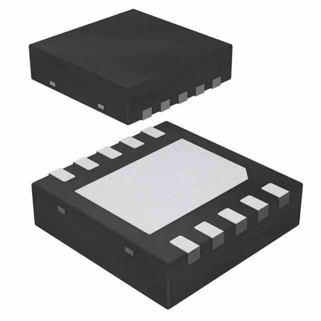
WSON (3 × 3 × 0.8 mm) Packaging
Create a custom design using the LMR10530 with
the WEBENCH® Power Designer
2 Applications
•
•
Point-of-load Conversions from 3.3-V and 5-V
Rails
Space-Constrained Applications
Device Information(1)
PART NUMBER
PACKAGE
LMR10530
WSON (10)
BODY SIZE (NOM)
3.00 mm × 3.00 mm
(1) For all available packages, see the orderable addendum at
the end of the data sheet.
Typical Application
9,10
VIN
SW
VIND
7,8
L1
VOUT
D1
R3
2
1
C1
R1
EN
LMR10530
FB
5
C2
VINC
NC
C3
SGND
3
4
R2
PGND
6
1
An IMPORTANT NOTICE at the end of this data sheet addresses availability, warranty, changes, use in safety-critical applications,
intellectual property matters and other important disclaimers. PRODUCTION DATA.
�LMR10530
SNVS814B – JUNE 2012 – REVISED JUNE 2019
www.ti.com
Table of Contents
1
2
3
4
5
6
7
Features ..................................................................
Applications ...........................................................
Description .............................................................
Revision History.....................................................
Pin Configuration and Functions .........................
Specifications.........................................................
1
1
1
2
3
4
6.1
6.2
6.3
6.4
4
4
5
6
Absolute Maximum Ratings ......................................
Recommended Operating Ratings............................
Electrical Characteristics...........................................
Typical Characteristics ..............................................
Detailed Description ............................................ 10
7.1 Overview ................................................................. 10
7.2 Functional Block Diagram ....................................... 11
7.3 Feature Description................................................. 12
8
Application and Implementation ........................ 16
8.1 Application Information............................................ 16
8.2 Typical Application ................................................. 16
9
Layout ................................................................... 26
9.1 Layout Considerations ............................................ 26
10 Device and Documentation Support ................. 27
10.1
10.2
10.3
10.4
10.5
10.6
Device Support......................................................
Receiving Notification of Documentation Updates
Community Resources..........................................
Trademarks ...........................................................
Electrostatic Discharge Caution ............................
Glossary ................................................................
27
27
27
27
27
28
11 Mechanical, Packaging, and Orderable
Information ........................................................... 28
4 Revision History
NOTE: Page numbers for previous revisions may differ from page numbers in the current version.
Changes from Revision A (April 2013) to Revision B
•
Editorial changes only; add WEBENCH links ........................................................................................................................ 1
Changes from Original (April 2013) to Revision A
•
2
Page
Page
Changed layout of National Semiconductor data sheet to TI format...................................................................................... 1
Submit Documentation Feedback
Copyright © 2012–2019, Texas Instruments Incorporated
Product Folder Links: LMR10530
�LMR10530
www.ti.com
SNVS814B – JUNE 2012 – REVISED JUNE 2019
5 Pin Configuration and Functions
DSC Package
10-Pin WSON
Top View
VINC
1
10
VIND
EN
2
9
VIND
SGND
3
8
SW
NC
4
7
SW
FB
5
6
PGND
DAP
Pin Descriptions
PIN
NO.
DESCRIPTION
NAME
1
VINC
Input supply for internal bias and control circuitry. Need to locally bypass this pin to GND.
2
EN
3
SGND
4
NC
No user function, connect this pin to GND.
5
FB
Feedback pin. Connect this pin to the external resistor divider to set output voltage.
6
PGND
7, 8
SW
9, 10
VIND
DAP
Die Attach Pad
Enable control input. Logic high enables operation. Do not allow this pin to float or subject to voltages
greater than VIN + 0.3V.
Signal (analog) ground. Place the bottom resistor of the feedback network as close as possible to this pin
for good load regulation.
Power ground pin. Provides ground return path for the internal driver.
Switch pins. Connect these pins to the inductor and catch diode.
Input supply voltage. Connect a bypass capacitor locally from these pins to PGND.
Connect to system ground for low thermal impedance, but it cannot be used as a primary GND
connection.
Submit Documentation Feedback
Copyright © 2012–2019, Texas Instruments Incorporated
Product Folder Links: LMR10530
3
�LMR10530
SNVS814B – JUNE 2012 – REVISED JUNE 2019
www.ti.com
6 Specifications
6.1 Absolute Maximum Ratings
See notes (1) (2).
VINC, VIND
-0.5V to 7V
FB Voltage
-0.5V to 3V
EN Voltage
-0.5V to VIN+o.3V
SW Voltage
-0.5V to 7V
ESD Susceptibility (3)
Junction Temperature
2kV
(4)
150°C
Storage Temperature
-65°C to +150°C
Soldering Information Infrared/Convection Reflow (15 sec)
(1)
(2)
(3)
(4)
220°C
Absolute Maximum Ratings indicate limits beyond which damage to the device may occur, including inoperability and degradation of
device reliability and/or performance. Functional operation of the device and/or non-degradation at the Absolute Maximum Ratings or
other conditions beyond those indicated in the recommended Operating Ratings is not implied. The recommended Operating Ratings
indicate conditions at which the device is functional and should not be operated beyond such conditions.
If Military/Aerospace specified devices are required, contact the Texas Instruments Sales Office/ Distributors for availability and
specifications.
Human body model, 1.5 kΩ in series with 100 pF.
Thermal shutdown occurs if the junction temperature exceeds the maximum junction temperature of the device.
6.2 Recommended Operating Ratings
VINC, VIND
3V to 5.5V
Junction Temperature
4
-40°C to +125°C
Submit Documentation Feedback
Copyright © 2012–2019, Texas Instruments Incorporated
Product Folder Links: LMR10530
�LMR10530
www.ti.com
SNVS814B – JUNE 2012 – REVISED JUNE 2019
6.3 Electrical Characteristics
Unless otherwise specified under the Conditions column, VIN = 5 V. Limits in standard type are for TJ = 25°C only; limits in
boldface type apply over the junction temperature (TJ) range of –40°C to +125°C. Minimum and Maximum limits are ensured
through test, design, or statistical correlation. Typical values represent the most likely parametric norm, and are provided for
reference purposes only.
PARAMETER
VFB
ΔVFB/(ΔVINxVFB)
IB
UVLO
TEST CONDITIONS
Feedback Voltage
WSON-10 Package
Feedback Voltage Line Regulation
VIN = 3V to 5.5V
MIN
TYP
MAX
0.588
0.600
0.612
0.08
Feedback Input Bias Current
VIN Rising
Undervoltage Lockout
VIN Falling
1.85
UVLO Hysteresis
Switching Frequency
DMAX
Maximum Duty Cycle
DMIN
Minimum Duty Cycle
RDS(ON)
ICL
VEN_TH
(1)
(2)
2.70
2.90
2.35
1.1
1.5
1.95
2.25
3.0
3.75
LMR10530X
86%
95%
LMR10530Y
80%
90%
5%
LMR10530Y
7%
58
3.4
Enable Threshold Voltage
1.8
Switch Leakage
Enable Pin Current
90
4.4
Shutdown Threshold Voltage
V
MHz
mΩ
A
0.4
100
Quiescent Current (switching)
nA
V
LMR10530Y
Switch Current Limit
IEN
VFB_F
100
LMR10530X
Switch On Resistance
ISW
IQ
0.1
LMR10530X
V
%/V
0.35
fSW
UNIT
V
nA
Sink/Source
100
LMR10530X, VFB = 0.55
3.2
5
nA
LMR10530Y, VFB = 0.55
4.3
6.5
mA
Quiescent Current (shutdown)
All Options VEN = 0V
300
nA
FB Frequency Foldback Threshold
All Options
0.32
V
LMR10530X, VFB = 0V
400
LMR10530Y, VFB = 0V
800
fFB
Foldback Frequency
θJA
Junction to Ambient
0 LFPM Air Flow (1)
θJC
Junction to Case
TSD
Thermal Shutdown Threshold
TSD_HYS
Thermal Shutdown Hysteresis
(1)
(2)
kHz
53
°C/W
12
°C/W
Junction Temperature
Rising
165
°C
Junction Temperature
Falling
15
°C
Applies for packages soldered directly onto a 4” × 3” 4-layer standard JEDEC board in still air.
Thermal shutdown occurs if the junction temperature exceeds the maximum junction temperature of the device.
Submit Documentation Feedback
Copyright © 2012–2019, Texas Instruments Incorporated
Product Folder Links: LMR10530
5
�LMR10530
SNVS814B – JUNE 2012 – REVISED JUNE 2019
www.ti.com
6.4 Typical Characteristics
Unless otherwise specified, VIN = 5 V and TA = 25°C
6
Figure 1. Efficiency vs Load Current - Both Options
Figure 2. Efficiency vs Load Current - LMR10530X
Figure 3. Efficiency vs Load Current - LMR10530Y
Figure 4. Oscillator Frequency vs Temperature - LMR10530X
Figure 5. Oscillator Frequency vs Temperature - LMR10530Y
Figure 6. Current Limit vs Temperature
Submit Documentation Feedback
Copyright © 2012–2019, Texas Instruments Incorporated
Product Folder Links: LMR10530
�LMR10530
www.ti.com
SNVS814B – JUNE 2012 – REVISED JUNE 2019
Typical Characteristics (continued)
Unless otherwise specified, VIN = 5 V and TA = 25°C
Figure 7. RDS(ON) vs Temperature
Figure 8. LMR10530X IQ (Switching)
Figure 9. LMR10530Y IQ (Switching)
Figure 10. VFB vs Temperature
Figure 11. Frequency Foldback
Figure 12. Loop Gain and Phase - LMR10530X
Submit Documentation Feedback
Copyright © 2012–2019, Texas Instruments Incorporated
Product Folder Links: LMR10530
7
�LMR10530
SNVS814B – JUNE 2012 – REVISED JUNE 2019
www.ti.com
Typical Characteristics (continued)
Unless otherwise specified, VIN = 5 V and TA = 25°C
8
Figure 13. Loop Gain And Phase - LMR10530Y
Figure 14. Load Step Response - LMR10530X
Figure 15. Start-up by EN - LMR10530X
Figure 16. Shutdown by EN - LMR10530X
Figure 17. Startup With EN Tied to VIN - LMR10530X
Figure 18. Short-Circuit Triggering - LMR10530X
Submit Documentation Feedback
Copyright © 2012–2019, Texas Instruments Incorporated
Product Folder Links: LMR10530
�LMR10530
www.ti.com
SNVS814B – JUNE 2012 – REVISED JUNE 2019
Typical Characteristics (continued)
Unless otherwise specified, VIN = 5 V and TA = 25°C
Figure 19. Short-Circuit Release - LMR10530X
Submit Documentation Feedback
Copyright © 2012–2019, Texas Instruments Incorporated
Product Folder Links: LMR10530
9
�LMR10530
SNVS814B – JUNE 2012 – REVISED JUNE 2019
www.ti.com
7 Detailed Description
7.1 Overview
The LMR10530 is a constant frequency PWM buck regulator IC that delivers a 3-A load current. The regulator is
available in preset switching frequencies of 1.5 MHz or 3 MHz. This high frequency allows the LMR10530 to
operate with small surface mount capacitors and inductors, resulting in a DC/DC converter that requires a
minimum amount of board space. The LMR10530 is internally compensated, therefore it is simple to use and
requires few external components. The LMR10530 uses peak current-mode control to regulate the output
voltage. The following description of operation of the LMR10530 will refer to the Figure 30, to the waveforms in
Figure 20 and simplified block diagram in Functional Block Diagram. The LMR10530 supplies a regulated output
voltage by switching the internal PMOS power switch at a constant frequency and variable duty cycle. A
switching cycle begins at the falling edge of the reset pulse generated by the internal oscillator. When this pulse
goes low, the output control logic turns on the internal PMOS power switch. During this on-time, the SW pin
voltage (VSW) swings up to approximately VIN, and the inductor current (IL) increases with a linear slope. IL is
measured by the current sense amplifier, which generates an output proportional to the switch current. The
sense signal is summed with the regulator’s corrective ramp and compared to the error amplifier’s output, which
is proportional to the difference between the feedback voltage and VREF. When the PWM comparator output goes
high, the internal power switch turns off until the next switching cycle begins. During the switch off-time, the
inductor current discharges through the catch diode D1, which forces the SW pin to swing below ground by the
forward voltage (VD) of the catch diode. The regulator loop adjusts the duty cycle (D) to maintain a constant
output voltage.
VSW
D = TON/TSW
VIN
SW
Voltage
TOFF
TON
0
-VD
IL
t
TSW
ILPK
IOUT
Inductor
Current
'iL
0
t
Figure 20. Typical Waveforms
10
Submit Documentation Feedback
Copyright © 2012–2019, Texas Instruments Incorporated
Product Folder Links: LMR10530
�LMR10530
www.ti.com
SNVS814B – JUNE 2012 – REVISED JUNE 2019
7.2 Functional Block Diagram
Submit Documentation Feedback
Copyright © 2012–2019, Texas Instruments Incorporated
Product Folder Links: LMR10530
11
�LMR10530
SNVS814B – JUNE 2012 – REVISED JUNE 2019
www.ti.com
7.3 Feature Description
7.3.1 Frequency Foldback
The LMR10530 uses frequency foldback to help limit switch current and power dissipation during start-up, shortcircuit and over load conditions by sensing if the feedback voltage is below 0.32 V (typical). The LMR10530
reduces the switching frequency from the nominal fixed value (1.5 MHz or 3 MHz) down to 400 kHz
(LMR10530X) or 800 kHz (LMR10530Y) when the feedback voltage drops to 0 V. See Figure 11 plot in the
Typical Characteristics section.
7.3.2 Load Step Response
The LMR10530 has a fixed internal loop compensation, which results in a small-signal loop bandwidth highly
related to the output voltage level. In general, the loop bandwidth at low voltage is larger than at high voltage due
to the increased overall loop gain. The limited bandwidth at high output voltage may pose a challenge when loop
step response is concerned. In this case, one effective approach to improving loop step response is to add a
feed-forward capacitor CFF) in the range of 27 nF to 100 nF in parallel with the upper feedback resistor
(assuming the lower feedback resistor is 2 kΩ), as shown in Figure 21. The feedforward capacitor introduces a
zero-pole pair which helps compensate the loop. The position of the zero-pole pair is a function of the feedback
resistors and capacitor:
(1)
(2)
Note the factor in parenthesis is the ratio of the output voltage to the feedback voltage. As the output voltage
gets close to 0.6V, the pole moves towards the zero, tending to cancel it out. Consequently, adding CFF will have
less effect on the step response at lower output voltages.
As an example, Figure 23 shows that at the output voltage of 3.3 V, 47 nF of CFF can boost the loop bandwidth
to 117kHz, from the original 23kHz as shown in Figure 22. Correspondingly, the responses to a load step
between 0.3 A and 3 A without and with CFF are shown in Figure 24 and Figure 25 respectively. The higher loop
bandwidth as a result of CFF reduces the total output excursion by more than half.
Aside from the above approach, increasing the output capacitance is generally also effective to reduce the
excursion in output voltage caused by a load step. This approach remains valid for applications where the
desired output voltages are close to the feedback voltage.
Figure 21. Adding a CFF Capacitor
12
Submit Documentation Feedback
Copyright © 2012–2019, Texas Instruments Incorporated
Product Folder Links: LMR10530
�LMR10530
www.ti.com
SNVS814B – JUNE 2012 – REVISED JUNE 2019
Feature Description (continued)
Figure 22. Loop Gain and Phase Without CFF
Figure 23. Loop Gain and Phase With CFF
Figure 24. Load Step Response Without CFF
Figure 25. Load Step Response With CFF
7.3.3 Output Overvoltage Protection
The LMR10530 has a builtin output overvoltage comparator that compares the FB pin voltage to a threshold
voltage that is 15% higher than the internal reference VREF. Once the FB pin voltage exceeds this threshold level
(typically 0.69 V), the internal PMOS power switch is turned off, which allows the output voltage to decrease
towards regulation.
7.3.4 Undervoltage Lockout
Undervoltage lockout (UVLO) prevents the LMR10530 from operating until the input voltage exceeds 2.7 V
(typical). The UVLO threshold has approximately 350 mV of hysteresis, so the device operates until VIN drops
below 2.35 V (typical). Hysteresis prevents the part from turning off during power up if VIN is non-monotonic.
Submit Documentation Feedback
Copyright © 2012–2019, Texas Instruments Incorporated
Product Folder Links: LMR10530
13
�LMR10530
SNVS814B – JUNE 2012 – REVISED JUNE 2019
www.ti.com
Feature Description (continued)
7.3.5 Current Limit
The LMR10530 uses cycle-by-cycle current limiting to protect the internal power switch. During each switching
cycle, a current limit comparator detects if the power switch current exceeds 4.4 A (typical), and turns off the
switch until the next switching cycle begins.
7.3.6 Soft Start/Shutdown
The LMR10530 has both enable and shutdown modes that are controlled by the EN pin. Connecting a voltage
source greater than 1.8 V to the EN pin enables the operation of the LMR10530, while reducing this voltage
below 0.4 V places the part in a low quiescent current (300 nA typical) shutdown mode. There is no internal pullup on EN pin, therefore an external signal is required to initiate switching. Do not allow this pin to float or rise to
0.3 V above VIN. It should be noted that when the EN pin voltage rises above 1.8 V while the input voltage is
greater than UVLO, there is 15-µs delay before switching starts. During this delay the LMR10530 goes through a
power on reset state after which the internal soft-start process commences. During soft-start, the error amplifier’s
reference voltage ramps from 0V to its nominal value of 0.6 V in approximately 600 µs. This forces the regulator
output to ramp up in a controlled fashion, which helps reduce inrush current seen at the input and minimizes
output voltage overshoot.
The simplest way to enable the operation of the LMR10530 is to connect the EN pin to VIN which allows self
start-up of the LMR10530 whenever the input voltage is applied. However, when an input voltage of slow rise
time is used to power the application and if both the input voltage and the output voltage are not fully established
before the soft-start time elapses, the control circuit commands maximum duty cycle operation of the internal
power switch to bring up the output voltage rapidly. When the feedback pin voltage exceeds 0.6 V, the duty cycle
will have to reduce from the maximum value accordingly, to maintain regulation. The reduction of duty cycle
takes a finite amount of time and can result in a transient in output voltage for a short duration, as shown in
Figure 26. In applications where this output voltage overshoot is undesirable, one simple solution is to add a
feed-forward capacitor CFF) across the top feedback resistor R1 to speed Gm Amplifier recovery. In practice, a
27-nF to 100-nF ceramic capacitor is usually a good choice to remove the overshoot completely or limit the
overshoot to an insignificant level during startup, as shown in Figure 27. Another more effective solution is to
control EN pin voltage by a separate logic signal, and pull the signal high only after VIN is fully established. In this
way, the chip can execute a normal, complete soft start process, minimizing any output voltage overshoot. Under
some circumstances at cold temperature, this approach may also be required to minimize any unwanted output
voltage transients that may occur when the input voltage rises slowly. For a fast rising input voltage (100 µs for
example), there is no need to control EN separately or add a feedforward capacitor since the soft start can bring
up output voltage smoothly as shown in Figure 28.
During startup, the LMR10530 gradually increases the switching frequency from 400 kHz (LMR10530X) or 800
kHz (LMR10530Y) to the nominal fixed value, as the feedback voltage increases (see Frequency Foldback
section for more information). Since the internal corrective ramp signal adjusts its slope dynamically, and is
proportional to the switching frequency during startup, a larger output capacitance may be required to insure a
smooth output voltage rise, at low programmed output voltage and high output load current.
14
Submit Documentation Feedback
Copyright © 2012–2019, Texas Instruments Incorporated
Product Folder Links: LMR10530
�LMR10530
www.ti.com
SNVS814B – JUNE 2012 – REVISED JUNE 2019
Feature Description (continued)
Figure 26. Start-up Response to VIN
Figure 27. Start-up Response to VIN With CFF
Figure 29. Recovery From Thermal Shutdown "LMR10530X"
Figure 28. Startup Response To VIN With 100-µs Rise Time
7.3.7 Thermal Shutdown
Thermal shutdown limits total power dissipation by turning off the internal power switch when the IC junction
temperature typically exceeds 165°C. After thermal shutdown occurs, the power switch does not turn on again
until the junction temperature drops below approximately 150°C.
Submit Documentation Feedback
Copyright © 2012–2019, Texas Instruments Incorporated
Product Folder Links: LMR10530
15
�LMR10530
SNVS814B – JUNE 2012 – REVISED JUNE 2019
www.ti.com
8 Application and Implementation
NOTE
Information in the following applications sections is not part of the TI component
specification, and TI does not warrant its accuracy or completeness. TI’s customers are
responsible for determining suitability of components for their purposes. Customers should
validate and test their design implementation to confirm system functionality.
8.1 Application Information
The LMR10530 regulator is a monolithic, high frequency, PWM step-down DC/DC converter available in a 10-pin
WSON package. It contains all the active functions to provide local DC/DC conversion with fast transient
response and accurate regulation in the smallest possible PCB area. With a minimum of external components,
the LMR10530 is easy to use. Switching frequency is internally set to 1.5 MHz or 3 MHz, allowing the use of
extremely small surface mount inductors and capacitors. Even though the operating frequency is high,
efficiencies up to 93% are easy to achieve.
8.2 Typical Application
EN
3.3 PH
(³;´ YHUVLRQ)
U1
R3
6
VIN
4, 5
2
EN
SW
1.0 PH
VINA/VIND
GND
VOUT
L1
3
FB
1
1.8V
R1
20k
C3
22 PF
C2
C1
2.2 PF
R2
10k
D1
2.2 PF
GND
C4
22 PF
Chf
22 nF
(opt.)
GND
Figure 30. Typical Application Schematic
8.2.1 Detailed Design Procedure
8.2.1.1 Custom Design With WEBENCH® Tools
Click here to create a custom design using the LMR10530 device with the WEBENCH® Power Designer.
1. Start by entering the input voltage (VIN), output voltage (VOUT), and output current (IOUT) requirements.
2. Optimize the design for key parameters such as efficiency, footprint, and cost using the optimizer dial.
3. Compare the generated design with other possible solutions from Texas Instruments.
The WEBENCH Power Designer provides a customized schematic along with a list of materials with real-time
pricing and component availability.
In most cases, these actions are available:
• Run electrical simulations to see important waveforms and circuit performance
• Run thermal simulations to understand board thermal performance
• Export customized schematic and layout into popular CAD formats
• Print PDF reports for the design, and share the design with colleagues
Get more information about WEBENCH tools at www.ti.com/WEBENCH.
16
Submit Documentation Feedback
Copyright © 2012–2019, Texas Instruments Incorporated
Product Folder Links: LMR10530
�LMR10530
www.ti.com
SNVS814B – JUNE 2012 – REVISED JUNE 2019
Typical Application (continued)
8.2.1.2 Inductor Selection
The duty cycle (D) can be approximated quickly using the ratio of output voltage (VOUT) to input voltage (VIN):
D=
VOUT
VIN
(3)
The catch diode (D1) forward voltage drop and the voltage drop across the internal PMOS must be included to
calculate a more accurate duty cycle. Calculate D by using the following formula:
D=
VOUT + VD
VIN + VD - VSW
(4)
VSW can be approximated by:
VSW = IOUT x RDS(ON)
where
•
IOUT is output load current.
(5)
The diode forward drop (VD) can range from 0.3 V to 0.7 V depending on the quality of the diode. The lower the
VD, the higher the operating efficiency of the converter.
The inductor value determines the output ripple current (ΔiL, as defined in ). Lower inductor values decrease the
size of the inductor, but increase the output ripple current. An increase in the inductor value decreases the output
ripple current. In general, the ratio of ripple current to the output current is optimized when it is set between 0.2
and 0.4 for output currents above 2 A. This ratio r is defined as:
r=
'iL
lOUT
(6)
One must ensure that the minimum current limit (3.4 A) is not exceeded, so the peak current in the inductor must
be calculated. The peak current (ILPK) in the inductor is calculated by:
ILPK = IOUT + ΔiL/2
(7)
When the designed maximum output current is reduced, the ratio r can be increased. At a current of 0.1 A, r can
be made as high as 0.9. The ripple ratio can be increased at lighter loads because the net ripple is actually quite
low, and if r remains constant the inductor value can be made quite large. An equation empirically developed for
the maximum ripple ratio at any current below 2 A is:
r = 0.387 x IOUT-0.3667
(8)
Note that this is just a guideline, and it needs to be combined with two important factors for proper selection of
inductance values at any operating condition. The first consideration is at output voltage above 2.5 V, one needs
to ensure that the inductance given by the above guideline should not be less than 1 µH for the LMR10530X or
0.5 µH for the LMR10530Y. Because the LMR10530 has a fixed internal corrective ramp signal, a very low
inductance value at high output voltage generates a very steep down slope of inductor current, which results in
an insufficient slope compensation, and cause instability known as sub-harmonic oscillation. Another
consideration is at low load current, one needs to ensure that the inductance value given by the guideline should
not exceed 10 µH for the LMR10530X and 4.7 µH for the LMR10530Y, since too much inductance effectively
flattens the down slope of the inductor current, and may significantly limit the system bandwidth and phase
margin resulting in instability.
The LMR10530 operates at frequencies allowing the use of ceramic output capacitors without compromising
transient response. Ceramic capacitors allow higher inductor ripple without significantly increasing output ripple.
See the Output Capacitor section for more details on calculating output voltage ripple.
Now that the ripple current is determined, the inductance is calculated by:
L=
VOUT + VD
IOUT x r x fSW
x (1-D)
where
•
fSW is the switching frequency.
(9)
Submit Documentation Feedback
Copyright © 2012–2019, Texas Instruments Incorporated
Product Folder Links: LMR10530
17
�LMR10530
SNVS814B – JUNE 2012 – REVISED JUNE 2019
www.ti.com
Typical Application (continued)
When selecting an inductor, make sure that it is capable of supporting the peak output current without saturating.
Inductor saturation will result in a sudden reduction in inductance and prevent the regulator from operating
properly. Because of the operating frequency of the LMR10530, ferrite based inductors are preferred to minimize
core losses. This presents little restriction since the variety and availability of ferrite-based inductors is large.
Lastly, inductors with lower series resistance (DCR) will provide better operating efficiency. For recommended
inductor selection, refer to Other System Examples.
8.2.1.3 Input Capacitor
An input capacitor is necessary to ensure that VIN does not drop excessively during switching transients. The
primary specifications of the input capacitor are capacitance, voltage rating, RMS current rating, and equivalent
series inductance (ESL). The input voltage rating is specifically stated by the capacitor manufacturer. Make sure
to check any recommended deratings and also verify if there is any significant change in capacitance at the
operating input voltage and the operating temperature. The input capacitor maximum RMS input current rating
(IRMS-IN) must be greater than:
2
IRMS-IN = IOUT x D x 1 - D + r
12
(10)
Neglecting inductor ripple simplifies the above equation to:
IRMS-IN = IOUT x D x 1 - D
(11)
It can be shown from the above equation that maximum RMS capacitor current occurs when D = 0.5. Always
calculate the RMS at the point where the duty cycle D is closest to 0.5. The ESL of an input capacitor is usually
determined by the effective cross sectional area of the current path. As a rule of thumb, a large leaded capacitor
will have high ESL and a 1206 ceramic chip capacitor will have very low ESL. At the operating frequencies of the
LMR10530, leaded capacitors may have an ESL so large that the resulting impedance (2 πfL) will be higher than
that required to provide stable operation. TI strongly recommends usin ceramic capacitors due to their low ESR
and low ESL. A 22-µF multilayer ceramic capacitor (MLCC) is a good choice for most applications. In cases
where large capacitance is required, use surface mount capacitors such as Tantalum capacitors and place at
least a 4.7-µF ceramic capacitor close to the VIN pin. For MLCCs TI recommends using X7R or X5R dielectrics.
Consult capacitor manufacturer datasheet to see how rated capacitance varies over operating conditions.
8.2.1.4 Output Capacitor
The output capacitor is selected based upon the desired output ripple and transient response. The initial current
of a load transient is provided mainly by the output capacitor. The output ripple of the converter is:
'VOUT = 'IL RESR +
1
8 x fSW x COUT
(12)
When using MLCCs, the ESR is typically so low that the capacitive ripple may dominate. When this occurs, the
output ripple will be approximately sinusoidal and 90° phase shifted from the switching action. Given the
availability and quality of MLCCs and the expected output voltage of designs using the LMR10530, there is really
no need to review any other capacitor technologies. Another benefit of ceramic capacitors is their ability to
bypass high frequency noise. A certain amount of switching edge noise will couple through parasitic
capacitances in the inductor to the output. A ceramic capacitor will bypass this noise while a tantalum will not.
Since the output capacitor is one of the two external components that control the stability of the regulator control
loop, most applications will require a minimum of 22-µF output capacitance. In the case of low output voltage, a
larger output capacitance is required to ensure sufficient phase margin. Capacitance can often, but not always,
be increased significantly with little detriment to the regulator stability. Like the input capacitor, recommended
multilayer ceramic capacitors are X7R or X5R types. Again, verify actual capacitance at the desired operating
voltage and temperature. Check the RMS current rating of the capacitor. The maximum RMS current rating of the
capacitor is:
(13)
One may select a 1206 size MLCC for output capacitor, since its current rating is typically above 1 A, more than
enough for the requirement.
18
Submit Documentation Feedback
Copyright © 2012–2019, Texas Instruments Incorporated
Product Folder Links: LMR10530
�LMR10530
www.ti.com
SNVS814B – JUNE 2012 – REVISED JUNE 2019
Typical Application (continued)
8.2.1.5 Catch Diode
The catch diode conducts during the switch off-time. TI recommends a Schottky diode for its fast switching time
and low forward voltage drop. The catch diode should be chosen such that its current rating is greater than:
ID = IOUT × (1-D)
(14)
The reverse breakdown rating of the diode must be at least the maximum input voltage plus appropriate margin.
To improve efficiency, choose a Schottky diode with a low forward voltage drop.
8.2.1.6 Output Voltage
The output voltage is set using the following equation where R2 is connected between the FB pin and GND, and
R1 is connected between VOUT and the FB pin. A good value for R2 is 2 kΩ.
VOUT
R1 =
VREF
- 1 x R2
(15)
(16)
VREF = 0.6 V
8.2.1.7
Efficiency Estimation
The complete LMR10530 DC/DC converter efficiency can be calculated in the following manner:
K=
POUT
PIN
(17)
or
K=
POUT
POUT + PLOSS
(18)
Calculations for determining the most significant power losses are shown in the following examples. Other losses
totaling less than 2% are not discussed.
The main power loss (PLOSS) in the converter includes two basic types of losses: switching loss and conduction
loss. In addition, there is loss associated with the power required for the internal circuitry of IC. Conduction
losses usually dominate at higher output loads, whereas switching losses dominate at lower output loads. The
first step in determining the losses is to calculate the duty cycle (D):
D=
VOUT + VD
VIN + VD - VSW
(19)
VSW is the voltage drop across the internal power switch when it is on, and is equal to:
VSW = IOUT × RDS(ON)
(20)
VD is the forward voltage drop across the catch diode. It can be obtained from the diode manufactures Electrical
Characteristics section. If the DC voltage drop across the inductor (VDCR) is accounted for, the equation
becomes:
D=
VOUT + VD + VDCR
VIN + VD - VSW
(21)
The conduction losses in the catch diode are calculated as follows:
PDIODE = VD × IOUT × (1-D)
(22)
Often this is the single most significant power loss in the circuit. Take care to choose a Schottky diode with a low
forward-voltage drop.
Another significant external power loss is the conduction loss in the output inductor. The equation can be
simplified to:
PIND = IOUT2 × RDCR
(23)
The LMR10530 conduction loss is mainly associated with the internal power switch:
Submit Documentation Feedback
Copyright © 2012–2019, Texas Instruments Incorporated
Product Folder Links: LMR10530
19
�LMR10530
SNVS814B – JUNE 2012 – REVISED JUNE 2019
www.ti.com
Typical Application (continued)
2
PCOND = (IOUT x D) x 1 +
'iL
1
x
3
IOUT
2
x RDS (ON)
(24)
If the inductor ripple current is fairly small, the conduction losses can be simplified to:
PCOND = IOUT2 × RDS(ON) x D
(25)
Switching losses are also associated with the internal power switch. They occur during the switch on and off
transition periods, where voltages and currents overlap resulting in power loss. The simplest means to determine
this loss is to empirically measuring the rise and fall times (10% to 90%) of the switch at the switch node.
Switching Power Loss is calculated as follows:
PSWR = 0.5 × (VIN × IOUT × fSW × TRISE)
PSWF = 0.5 × (VIN × IOUT × fSW × TFALL)
PSW = PSWR + PSWF
(26)
(27)
(28)
The power loss required for operation of the internal circuitry is given by:
PQ = IQ × VIN
(29)
IQ is the quiescent operating current, and is typically around 3.2 mA for the LMR10530X, and 4.3 mA for the
LMR10530Y.
An example of efficiency calculation for a typical application is shown in Table 1:
Table 1. Power Loss Tabulation
CONDITIONS
POWER LOSS
VIN
5V
VOUT
3.3 V
IOUT
3A
POUT
9.9 W
VD
0.33 V
PDIODE
277 mW
RDS(ON)
56 mΩ
PCOND
363 mW
PSW
225 mW
fSW
1.5 MHz
TRISE
10 ns
TFALL
10 ns
INDDCR
28 mΩ
PIND
252 mW
IQ
3.2 mA
PQ
16 mW
η
89.7%
D is calculated to be 0.72
PLOSS = Σ ( PCOND + PSW + PQ + PIND + PDIODE )
PLOSS = 1.133W
20
Submit Documentation Feedback
(30)
(31)
Copyright © 2012–2019, Texas Instruments Incorporated
Product Folder Links: LMR10530
�LMR10530
www.ti.com
SNVS814B – JUNE 2012 – REVISED JUNE 2019
8.2.2 Application Curve
Figure 31. Line Transient Response - "LMR10530X"
Submit Documentation Feedback
Copyright © 2012–2019, Texas Instruments Incorporated
Product Folder Links: LMR10530
21
�LMR10530
SNVS814B – JUNE 2012 – REVISED JUNE 2019
www.ti.com
8.2.3 Other System Examples
8.2.3.1 LMR10530X Design Example 1
VIN
9,10
SW
VIND
L1
7,8
VOUT
D1
R3
2
1
C1
R1
EN
LMR10530X
FB
VINC
C3
NC
SGND
3
5
C2
4
R2
PGND
6
VIN = 3.3 V
VOUT = 1.2 V
IOUT = 3 A
Figure 32. LMR10530X (1.5 MHz)
Table 2. Bill Of Materials
22
DEVICE ID
DEVICE VALUE
MANUFACTURER
U1
3-A buck regulator
TI
DEVICE NUMBER
LMR10530X
C1, Input Capacitor
22 µF, 6.3 V, X5R
TDK
C3216X5R0J226M
C2, Output Capacitor
47 µF, 6.3 V, X5R
TDK
C3216X5R0J476M
C3, Bypass Capacitor
0.22 µF, 10 V, X7R
Murata
GRM216R71A224KC01D
D1, Catch Diode
Schottky, 0.33 V at 3 A, VR= 30
V
Toshiba
CMS01
L1
1.8 µH, 3.6 A
TDK
LTF5022T-1R8N3R6
R1
2 kΩ, 1%
Vishay
CRCW08052K00FKEA
R2
2 kΩ, 1%
Vishay
CRCW08052K00FKEA
R3
10 Ω, 1%
Vishay
CRCW080510R0FKEA
Submit Documentation Feedback
Copyright © 2012–2019, Texas Instruments Incorporated
Product Folder Links: LMR10530
�LMR10530
www.ti.com
SNVS814B – JUNE 2012 – REVISED JUNE 2019
8.2.3.2 LMR10530X Design Example 2
VIN = 5 V
VOUT = 3.3 V
IOUT = 3 A
Figure 33. LMR10530X (1.5 MHz)
Table 3. Bill Of Materials
DEVICE ID
DEVICE VALUE
MANUFACTURER
DEVICE NUMBER
U1
3-A buck regulator
TI
LMR10530X
C1, Input Capacitor
22 µF, 6.3 V, X5R
TDK
C3216X5R0J226M
C2, Output Cap
47 µF, 6.3 V, X5R
TDK
C3216X5R0J476M
C3, Bypass Capacitor
0.22 µF, 10 V, X7R
Murata
GRM216R71A224KC01D
0805ZC473JAZ2A
CFF, Feed-forward Capacitor
47 nF, 10 V, X7R
AVX
D1, Catch Diode
Schottky, 0.43 V at 3 A, VR= 30 V
Vishay
SSA33L-E3/61T
L1
1.2 µH, 4.2 A
TDK
LTF5022T-1R2N4R2
R1
10.2 kΩ, 1%
Vishay
CRCW080510K2FKEA
R2
2.26 kΩ, 1%
Vishay
CRCW08052K26FKEA
R3
10 Ω, 1%
Vishay
CRCW080510R0FKEA
Submit Documentation Feedback
Copyright © 2012–2019, Texas Instruments Incorporated
Product Folder Links: LMR10530
23
�LMR10530
SNVS814B – JUNE 2012 – REVISED JUNE 2019
www.ti.com
8.2.3.3 LMR10530Y Design Example 3
VIN
9,10
SW
VIND
L1
7,8
VOUT
D1
R3
2
1
C1
R1
EN
LMR10530Y
FB
VINC
C3
NC
SGND
3
5
C2
4
R2
PGND
6
VIN = 3.3 V
VOUT = 1.2 V
IOUT = 3 A
Figure 34. LMR10530Y (3 MHz)
Table 4. Bill Of Materials
24
DEVICE ID
DEVICE VALUE
MANUFACTURER
U1
3-A buck regulator
TI
DEVICE NUMBER
LMR10530Y
C1, Input Capacitor
22 µF, 6.3 V, X5R
TDK
C3216X5R0J226M
C2, Output Capacitor
47µF, 6.3 V, X5R
TDK
C3216X5R0J476M
C3, Bypass Capacitor
0.22µF, 10 V, X7R
Murata
GRM216R71A224KC01D
D1, Catch Diode
Schottky, 0.33 V at 3 A, VR= 30
V
Toshiba
CMS01
L1
1 µH, 4 A
Taiyo Yuden
NP04SZB1R0N
R1
2 kΩ, 1%
Vishay
CRCW08052K00FKEA
R2
2 kΩ, 1%
Vishay
CRCW08052K00FKEA
R3
10 Ω, 1%
Vishay
CRCW080510R0FKEA
Submit Documentation Feedback
Copyright © 2012–2019, Texas Instruments Incorporated
Product Folder Links: LMR10530
�LMR10530
www.ti.com
SNVS814B – JUNE 2012 – REVISED JUNE 2019
8.2.3.4 LMR10530Y Design Example 4
VIN = 5 V
VOUT = 3.3 V
IOUT = 3 A
Figure 35. LMR10530Y (3 MHz)
Table 5. Bill Of Materials
DEVICE ID
DEVICE VALUE
MANUFACTURER
U1
3-A buck regulator
TI
DEVICE NUMBER
LMR10530Y
C1, Input Capacitor
22 µF, 6.3 V, X5R
TDK
C3216X5R0J226M
C2, Output Capacitor
47 µF, 6.3 V, X5R
TDK
C3216X5R0J476M
C3, Bypass Capacitor
0.22 µF, 10 V, X7R
Murata
GRM216R71A224KC01D
CFF, Feedforward Capacitor
47 nF, 10 V, X7R
AVX
0805ZC473JAZ2A
D1, Catch Diode
Schottky, 0.43 V at 3 A, VR= 30
V
Vishay
SSA33L-E3/61T
L1
1 µH, 4 A
Taiyo Yuden
NP04SZB1R0N
R1
10.2 kΩ, 1%
Vishay
CRCW080510K2FKEA
R2
2.26 kΩ, 1%
Vishay
CRCW08052K26FKEA
R3
10 Ω, 1%
Vishay
CRCW080510R0FKEA
Submit Documentation Feedback
Copyright © 2012–2019, Texas Instruments Incorporated
Product Folder Links: LMR10530
25
�LMR10530
SNVS814B – JUNE 2012 – REVISED JUNE 2019
www.ti.com
9 Layout
9.1 Layout Considerations
When planning layout there are a few things to consider to achieve a clean, regulated output. The most important
consideration is the close coupling of the GND connections of the input capacitor Cin and the catch diode D1.
These ground ends should be close to one another and be connected to the GND plane with at least two
through-holes. Place these components as close to the IC as possible. The next consideration is the location of
the GND connection of the output capacitor Co, which should be near the GND connections of C1 and D1. There
must be a continuous ground plane on the bottom layer of a two-layer board except under the switching node
island. Tie the signal ground SGND (pin 3) and power ground PGND (pin 6) together and connected to ground
plane through vias.
The FB pin is a high impedance node—take care to make the FB trace short to avoid noise pickup that causes
inaccurate regulation. The feedback resistors must be placed as close as possible to the IC, with the GND of
Rfbb placed as close as possible to the SGND of the IC. Route the VOUT trace to Rfb1 away from the inductor
and any other traces that are switching.
High AC currents flow through the VIN, SW, and VOUT traces, so they must be as short and wide as possible.
Radiated noise can be decreased by choosing a shielded inductor.
Place the remaining components as close as possible to the IC. See Application Note AN-2280 for further
considerations and the LMR10530 demo board as an example of a four-layer layout.
26
Submit Documentation Feedback
Copyright © 2012–2019, Texas Instruments Incorporated
Product Folder Links: LMR10530
�LMR10530
www.ti.com
SNVS814B – JUNE 2012 – REVISED JUNE 2019
10 Device and Documentation Support
10.1 Device Support
10.1.1 Third-Party Products Disclaimer
TI'S PUBLICATION OF INFORMATION REGARDING THIRD-PARTY PRODUCTS OR SERVICES DOES NOT
CONSTITUTE AN ENDORSEMENT REGARDING THE SUITABILITY OF SUCH PRODUCTS OR SERVICES
OR A WARRANTY, REPRESENTATION OR ENDORSEMENT OF SUCH PRODUCTS OR SERVICES, EITHER
ALONE OR IN COMBINATION WITH ANY TI PRODUCT OR SERVICE.
10.1.2 Development Support
10.1.2.1 Custom Design With WEBENCH® Tools
Click here to create a custom design using the LMR10530 device with the WEBENCH® Power Designer.
1. Start by entering the input voltage (VIN), output voltage (VOUT), and output current (IOUT) requirements.
2. Optimize the design for key parameters such as efficiency, footprint, and cost using the optimizer dial.
3. Compare the generated design with other possible solutions from Texas Instruments.
The WEBENCH Power Designer provides a customized schematic along with a list of materials with real-time
pricing and component availability.
In most cases, these actions are available:
• Run electrical simulations to see important waveforms and circuit performance
• Run thermal simulations to understand board thermal performance
• Export customized schematic and layout into popular CAD formats
• Print PDF reports for the design, and share the design with colleagues
Get more information about WEBENCH tools at www.ti.com/WEBENCH.
10.2 Receiving Notification of Documentation Updates
To receive notification of documentation updates, navigate to the device product folder on ti.com. In the upper
right corner, click on Alert me to register and receive a weekly digest of any product information that has
changed. For change details, review the revision history included in any revised document.
10.3 Community Resources
The following links connect to TI community resources. Linked contents are provided "AS IS" by the respective
contributors. They do not constitute TI specifications and do not necessarily reflect TI's views; see TI's Terms of
Use.
TI E2E™ Online Community TI's Engineer-to-Engineer (E2E) Community. Created to foster collaboration
among engineers. At e2e.ti.com, you can ask questions, share knowledge, explore ideas and help
solve problems with fellow engineers.
Design Support TI's Design Support Quickly find helpful E2E forums along with design support tools and
contact information for technical support.
10.4 Trademarks
E2E is a trademark of Texas Instruments.
WEBENCH is a registered trademark of Texas Instruments.
All other trademarks are the property of their respective owners.
10.5 Electrostatic Discharge Caution
This integrated circuit can be damaged by ESD. Texas Instruments recommends that all integrated circuits be handled with
appropriate precautions. Failure to observe proper handling and installation procedures can cause damage.
ESD damage can range from subtle performance degradation to complete device failure. Precision integrated circuits may be more
susceptible to damage because very small parametric changes could cause the device not to meet its published specifications.
Submit Documentation Feedback
Copyright © 2012–2019, Texas Instruments Incorporated
Product Folder Links: LMR10530
27
�LMR10530
SNVS814B – JUNE 2012 – REVISED JUNE 2019
www.ti.com
10.6 Glossary
SLYZ022 — TI Glossary.
This glossary lists and explains terms, acronyms, and definitions.
11 Mechanical, Packaging, and Orderable Information
The following pages include mechanical, packaging, and orderable information. This information is the most
current data available for the designated devices. This data is subject to change without notice and revision of
this document. For browser-based versions of this data sheet, refer to the left-hand navigation.
28
Submit Documentation Feedback
Copyright © 2012–2019, Texas Instruments Incorporated
Product Folder Links: LMR10530
�PACKAGE OPTION ADDENDUM
www.ti.com
10-Dec-2020
PACKAGING INFORMATION
Orderable Device
Status
(1)
Package Type Package Pins Package
Drawing
Qty
Eco Plan
(2)
Lead finish/
Ball material
MSL Peak Temp
Op Temp (°C)
Device Marking
(3)
(4/5)
(6)
LMR10530XSD/NOPB
ACTIVE
WSON
DSC
10
1000
RoHS & Green
SN
Level-1-260C-UNLIM
-40 to 125
L287B
LMR10530XSDX/NOPB
ACTIVE
WSON
DSC
10
4500
RoHS & Green
SN
Level-1-260C-UNLIM
-40 to 125
L287B
LMR10530YSD/NOPB
ACTIVE
WSON
DSC
10
1000
RoHS & Green
SN
Level-1-260C-UNLIM
-40 to 125
L286B
LMR10530YSDX/NOPB
ACTIVE
WSON
DSC
10
4500
RoHS & Green
SN
Level-1-260C-UNLIM
-40 to 125
L286B
(1)
The marketing status values are defined as follows:
ACTIVE: Product device recommended for new designs.
LIFEBUY: TI has announced that the device will be discontinued, and a lifetime-buy period is in effect.
NRND: Not recommended for new designs. Device is in production to support existing customers, but TI does not recommend using this part in a new design.
PREVIEW: Device has been announced but is not in production. Samples may or may not be available.
OBSOLETE: TI has discontinued the production of the device.
(2)
RoHS: TI defines "RoHS" to mean semiconductor products that are compliant with the current EU RoHS requirements for all 10 RoHS substances, including the requirement that RoHS substance
do not exceed 0.1% by weight in homogeneous materials. Where designed to be soldered at high temperatures, "RoHS" products are suitable for use in specified lead-free processes. TI may
reference these types of products as "Pb-Free".
RoHS Exempt: TI defines "RoHS Exempt" to mean products that contain lead but are compliant with EU RoHS pursuant to a specific EU RoHS exemption.
Green: TI defines "Green" to mean the content of Chlorine (Cl) and Bromine (Br) based flame retardants meet JS709B low halogen requirements of


 工商网监
湘ICP备2023018690号
工商网监
湘ICP备2023018690号
