LMR12010YMKDEMO/NOPB 数据手册
www.ti.com
Table of Contents
User’s Guide
LMR12010 Step-Down Converter Evaluation Module
User's Guide
Table of Contents
1 Introduction.............................................................................................................................................................................2
2 Features...................................................................................................................................................................................2
3 Enable Operation.................................................................................................................................................................... 2
4 Adjusting the Output Voltage................................................................................................................................................ 2
5 Test Setup................................................................................................................................................................................4
6 Typical Performance Characteristics....................................................................................................................................6
7 Layout...................................................................................................................................................................................... 7
8 Additional Circuit Configuration Schematics.................................................................................................................... 10
9 Revision History....................................................................................................................................................................11
Trademarks
All trademarks are the property of their respective owners.
SNVA490B – SEPTEMBER 2011 – REVISED DECEMBER 2021
LMR12010 Step-Down Converter Evaluation Module User's Guide
Submit Document Feedback
Copyright © 2021 Texas Instruments Incorporated
1
�Introduction
www.ti.com
1 Introduction
The LMR12010 is a step down DC-DC regulator that operates at the following switching frequencies: the
LMR12010X at 1.6 MHz and the LMR12010Y at 3 MHz. The demo board is configured to convert 5-V input to
1.8-V output at 1-A load current using the Y version. The tiny low profile thin SOT23 package allows the design
to use less than 1 square inch of board area.
The circuit is configured with the boost diode connected to VIN. VIN must not exceed the maximum operating
limit of 5.5 V + VfD2 using this configuration. This makes sure that the voltage between the boost and SW pins,
VBOOST – VSW, does not exceed 5.5 V for proper operation. For more information regarding this requirement, see
the LMR12010 SIMPLE SWITCHER® 20Vin, 1A Step-Down Voltage Regulator in SOT-23 Data Sheet.
The schematics at the end of this document show how to reconfigure this demo board for various input
and output conditions as discussed in the LMR12010 SIMPLE SWITCHER® 20Vin, 1A Step-Down Voltage
Regulator in SOT-23 Data Sheet. Short or leave open the connections as indicated in the schematics. The
previously mentioned restrictions for the input voltage are valid only for the demo board as shipped with the
demo board schematic shown in Figure 4-3
2 Features
•
•
•
•
•
3.0-V to 5-V input voltage range (as shipped)
1.8-V output voltage
Up to 1-A output current
Switching frequency of 3 MHz
Small solution size (17 mm × 17 mm)
3 Enable Operation
The demo board includes a spot for a pullup resistor R5 (not stuffed) to enable the device once VIN has
exceeded 1.8 V (typical). A typical value for this resistor is 100 KΩ. Otherwise, use the EN post to apply a logic
signal to test start-up and shutdown of the device. Never allow the EN voltage to exceed VIN.
4 Adjusting the Output Voltage
The output voltage can be changed from 1.8V to another voltage by adjusting the feedback resistors using
Equation 1:
VOUT = VFB(1 + (RFBT / RFBB))
(1)
where
• VFB is 0.8 V.
For more information on component selection and features, see the device-specific data sheet.
2
LMR12010 Step-Down Converter Evaluation Module User's Guide
SNVA490B – SEPTEMBER 2011 – REVISED DECEMBER 2021
Submit Document Feedback
Copyright © 2021 Texas Instruments Incorporated
�www.ti.com
Adjusting the Output Voltage
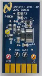
Figure 4-2. LMR12010 Demo Board Bottom View
Figure 4-1. LMR12010 Demo Board Top View
C4
D3
R3
D2
R4
VIN
VIN
C1
BOOST
C3
R5
L1
VOUT
SW
D1
EN
C2
EN
R1
FB
GND
R2
GND
GND
Figure 4-3. LMR12010Y Demo Board Schematic
Table 4-1. Bill of Materials (BOM) for LMR12010Y
Part ID
Part Value
Manufacturer
Part Number
Package Type
U1
1-A Buck Regulator
Texas Instruments
LMR12010
Thin SOT23-6
C1, Input Cap
10 µF, 10 V, X5R
Murata
GRM316R61A475KE19D
1206
C2, Output Cap
10 µF, 6.3 V, X5R
Murata
GRM319R60J106KE01D
1206
C3, Boost Cap
0.01 µF
Vishay
VJ0805Y103KXAAC
0805
D1, Catch Diode
0.45 Vf Schottky 1 A, 20VR
Vishay
MBRA120TRPBF
SMA
SNVA490B – SEPTEMBER 2011 – REVISED DECEMBER 2021
LMR12010 Step-Down Converter Evaluation Module User's Guide
Submit Document Feedback
Copyright © 2021 Texas Instruments Incorporated
3
�Test Setup
www.ti.com
Table 4-1. Bill of Materials (BOM) for LMR12010Y (continued)
Part ID
Part Value
Manufacturer
Part Number
Package Type
D2, Boost Diode
1 Vf at 50-mA Diode
L1
2.7 µH, 1.8 A, 33 mΩ
Diodes, Inc.
1N4148W-7-F
SOD-123
TDK
VLCF5028T-2R7N1R8-2
6028
R1
R2
12.4 kΩ, 1%
Vishay
CRCW080512K4FKEA
0805
10 kΩ, 1%
Vishay
CRCW080510K0FKEA
0805
R3
0Ω
Vishay
CRCW08050000Z0EA
0805
D3, C4, R4, R5
Open
5 Test Setup
Table 5-1. Demonstration Board Quick Setup Procedures
Step
Description
1
Connect a power supply to VIN terminals.
Notes
2
Connect a load to VO terminals.
3
EN should be connected to VIN for normal operation. Short this to ground to shut
down the part.
4
Set VIN = 5 V, with 0-A load applied. Check VO with a voltmeter.
Nominal 1.8 V
5
Apply a 1-A load and check VO.
Nominal 1.8 V
Ammeter
A
+
VOUT GND
Ammeter
A
GND
Voltmeter V
+
-
Electronic
Load
Power
Supply
Oscilloscope
VIN
V
Voltmeter
VO
GND
C2
Figure 5-2. Voltage Ripple Measurements
Demo Board
Figure 5-1. Efficiency Measurements
4
LMR12010 Step-Down Converter Evaluation Module User's Guide
SNVA490B – SEPTEMBER 2011 – REVISED DECEMBER 2021
Submit Document Feedback
Copyright © 2021 Texas Instruments Incorporated
�www.ti.com
Test Setup
I
I
I
VIN
I
I
I
I
GND
I
I
I
I
I
VOUT
75
86
9
10
A
B
A
C
B
D
CE
D
F
E
H
FJ
K
L
SPARE
46
VOUT SENSE+
53
VOUT SENSE -
42
VIN SENSE -
13
VIN SENSE+
2
EN
1
Figure 5-3. Edge Connector Schematic
SNVA490B – SEPTEMBER 2011 – REVISED DECEMBER 2021
LMR12010 Step-Down Converter Evaluation Module User's Guide
Submit Document Feedback
Copyright © 2021 Texas Instruments Incorporated
5
�Typical Performance Characteristics
www.ti.com
6 Typical Performance Characteristics
90
EFFICIENCY (%)
80
70
VOUT
100 mV/Div
IOUT
500 mA/Div
60
50
40
VIN =3.3V
VIN =5.0V
30
0.0 0.1 0.2 0.3 0.4 0.5 0.6 0.7 0.8 0.9 1.0
LOAD CURRENT (A)
Figure 6-1. Efficiency vs. Load Current
LMR12010Y, VO = 1.8 V
200 Ps/DIV
Figure 6-2. Load Transient Waveforms LMR12010Y,
IOUT = 100 mA to 1000 mA
10 mV/Div
VOUT
EN
SWITCH NODE
2V/Div
500 ns/DIV
1V/DIV
VOUT
1V/DIV
200 Ps/DIV
Figure 6-4. Start-Up Waveform
Figure 6-3. Switching Node and Output Voltage
Waveforms
6
LMR12010 Step-Down Converter Evaluation Module User's Guide
SNVA490B – SEPTEMBER 2011 – REVISED DECEMBER 2021
Submit Document Feedback
Copyright © 2021 Texas Instruments Incorporated
�www.ti.com
Layout
7 Layout
Figure 7-1. Top Layer
Figure 7-2. Top Overlay
SNVA490B – SEPTEMBER 2011 – REVISED DECEMBER 2021
LMR12010 Step-Down Converter Evaluation Module User's Guide
Submit Document Feedback
Copyright © 2021 Texas Instruments Incorporated
7
�Layout
www.ti.com
Figure 7-3. Inner Layer 1
8
LMR12010 Step-Down Converter Evaluation Module User's Guide
Figure 7-4. Inner Layer 2
SNVA490B – SEPTEMBER 2011 – REVISED DECEMBER 2021
Submit Document Feedback
Copyright © 2021 Texas Instruments Incorporated
�www.ti.com
Layout
Figure 7-5. Bottom Layer
Figure 7-6. Bottom Overlay
SNVA490B – SEPTEMBER 2011 – REVISED DECEMBER 2021
LMR12010 Step-Down Converter Evaluation Module User's Guide
Submit Document Feedback
Copyright © 2021 Texas Instruments Incorporated
9
�Additional Circuit Configuration Schematics
www.ti.com
8 Additional Circuit Configuration Schematics
C4
D3
R3
D2
VIN
R4
BOOST
VIN
C1
C3
R5
L1
VOUT
SW
D1
EN
C2
EN
R1
FB
GND
R2
GND
GND
Figure 8-1. VBOOST Derived from VOUT
D3
C4
R3
D2
VIN
R4
BOOST
VIN
C1
C3
R5
L1
VOUT
SW
D1
EN
C2
EN
R1
FB
GND
R2
GND
GND
Figure 8-2. VBOOST Derived from VSHUNT
10
LMR12010 Step-Down Converter Evaluation Module User's Guide
SNVA490B – SEPTEMBER 2011 – REVISED DECEMBER 2021
Submit Document Feedback
Copyright © 2021 Texas Instruments Incorporated
�www.ti.com
Revision History
D3
C4
R3
D2
VIN
R4
BOOST
VIN
C1
C3
R5
L1
VOUT
SW
D1
EN
C2
EN
R1
FB
GND
R2
GND
GND
Figure 8-3. VBOOST Derived from Series Zener Diode (VIN)
D3
C4
R3
D2
VIN
R4
BOOST
VIN
C3
C1
R5
L1
VOUT
SW
D1
EN
C2
EN
R1
FB
GND
R2
GND
GND
Figure 8-4. VBOOST Derived from Series Zener Diode (VOUT)
9 Revision History
NOTE: Page numbers for previous revisions may differ from page numbers in the current version.
Changes from Revision A (April 2013) to Revision B (December 2021)
Page
• Updated the numbering format for tables, figures, and cross-references throughout the document. ................2
• Updated the user's guide title............................................................................................................................. 2
• Edited user's guide for clarity..............................................................................................................................2
SNVA490B – SEPTEMBER 2011 – REVISED DECEMBER 2021
LMR12010 Step-Down Converter Evaluation Module User's Guide
Submit Document Feedback
Copyright © 2021 Texas Instruments Incorporated
11
�IMPORTANT NOTICE AND DISCLAIMER
TI PROVIDES TECHNICAL AND RELIABILITY DATA (INCLUDING DATA SHEETS), DESIGN RESOURCES (INCLUDING REFERENCE
DESIGNS), APPLICATION OR OTHER DESIGN ADVICE, WEB TOOLS, SAFETY INFORMATION, AND OTHER RESOURCES “AS IS”
AND WITH ALL FAULTS, AND DISCLAIMS ALL WARRANTIES, EXPRESS AND IMPLIED, INCLUDING WITHOUT LIMITATION ANY
IMPLIED WARRANTIES OF MERCHANTABILITY, FITNESS FOR A PARTICULAR PURPOSE OR NON-INFRINGEMENT OF THIRD
PARTY INTELLECTUAL PROPERTY RIGHTS.
These resources are intended for skilled developers designing with TI products. You are solely responsible for (1) selecting the appropriate
TI products for your application, (2) designing, validating and testing your application, and (3) ensuring your application meets applicable
standards, and any other safety, security, regulatory or other requirements.
These resources are subject to change without notice. TI grants you permission to use these resources only for development of an
application that uses the TI products described in the resource. Other reproduction and display of these resources is prohibited. No license
is granted to any other TI intellectual property right or to any third party intellectual property right. TI disclaims responsibility for, and you
will fully indemnify TI and its representatives against, any claims, damages, costs, losses, and liabilities arising out of your use of these
resources.
TI’s products are provided subject to TI’s Terms of Sale or other applicable terms available either on ti.com or provided in conjunction with
such TI products. TI’s provision of these resources does not expand or otherwise alter TI’s applicable warranties or warranty disclaimers for
TI products.
TI objects to and rejects any additional or different terms you may have proposed. IMPORTANT NOTICE
Mailing Address: Texas Instruments, Post Office Box 655303, Dallas, Texas 75265
Copyright © 2022, Texas Instruments Incorporated
�


 工商网监
湘ICP备2023018690号
工商网监
湘ICP备2023018690号
