LMR14006
SNVSA10B – NOVEMBER 2013 – REVISED NOVEMBER 2014
LMR14006 SIMPLE SWITCHER® 40 V 600 mA Buck Regulator With High Efficiency Sleep
Mode
1 Features
3 Description
•
•
•
•
•
•
•
•
•
•
•
•
The LMR14006 is a PWM DC/DC buck (step-down)
regulator. With a wide input range of 4 V-40 V, it is
suitable for a wide range of application from industrial
to automotive for power conditioning from an
unregulated source. The regulator’s standby current
is 28 µA in sleep mode, which is suitable for battery
operating systems. An ultra low 1 µA current can
further prolong battery life in shutdown mode.
Operating frequency is fixed at 1.1 MHz (X version)
and 2.1 MHz (Y version) allowing the use of small
external components while still being able to have low
output ripple voltage. Soft-start and compensation
circuits are implemented internally, and these allow
the device to be used with minimized external
components. The LMR14006 is optimized for up to
600 mA load current which has a 0.765 V typical
feedback voltage. The device has built-in protection
features such as pulse by pulse current limit, thermal
sensing and shutdown due to excessive power
dissipation. The LMR14006 is available in a low
profile TSOT-6L package.
1
Ultra Low 28 µA Standby Current in Sleep Mode
Input Voltage Range 4 V to 40 V
1 µA Shutdown Current
High Duty Cycle Operation Supported
Output Current up to 600 mA
1.1 MHz and 2.1 MHz Switching Frequency
Internal Compensation
High Voltage Enable Input
Internal Soft Start
Over Current Protection
Over Temperature Protection
Small Overall Solution Size (TSOT-6L Package)
2 Applications
•
•
•
•
•
Industrial Distributed Power Systems
Automotive
Battery Powered Equipment
Portable Handheld Instruments
Portable Media Players
Device Information(1)
PART NUMBER
PACKAGE
BODY SIZE (NOM)
LMR14006
TSOT-6L
2.9mm × 1.6 mm
(1) For all available packages, see the orderable addendum at
the end of the datasheet.
VIN
VIN
CB
Cboot L1
Cin
SW
SHDN
LMR14006
Cout
D1
R1
GND
FB
R2
Figure 1. Typical Application Schematic
1
An IMPORTANT NOTICE at the end of this data sheet addresses availability, warranty, changes, use in safety-critical applications,
intellectual property matters and other important disclaimers. PRODUCTION DATA.
�LMR14006
SNVSA10B – NOVEMBER 2013 – REVISED NOVEMBER 2014
www.ti.com
Table of Contents
1
2
3
4
5
6
Features ..................................................................
Applications ...........................................................
Description .............................................................
Revision History.....................................................
Pin Configuration and Functions .........................
Specifications.........................................................
1
1
1
2
3
4
6.1
6.2
6.3
6.4
6.5
6.6
6.7
4
4
4
4
5
5
6
Absolute Maximum Ratings ......................................
Handling Ratings ......................................................
Recommended Operating Conditions .....................
Thermal Information ..................................................
Electrical Characteristics...........................................
Switching Characteristics ..........................................
Typical Characteristics ..............................................
7
Detailed Description .............................................. 8
7.1 Overview ................................................................... 8
7.2 Functional Block Diagram ......................................... 8
7.3 Feature Description................................................... 8
8
Applications and Implementation ...................... 11
9
Layout ................................................................... 16
8.1 Typical Applications ................................................ 11
9.1 Layout Guidelines ................................................... 16
10 Device and Documentation Support ................. 17
10.1 Trademarks ........................................................... 17
10.2 Electrostatic Discharge Caution ............................ 17
10.3 Glossary ................................................................ 17
11 Mechanical, Packaging, and Orderable
Information ........................................................... 17
4 Revision History
NOTE: Page numbers for previous revisions may differ from page numbers in the current version.
Changes from Original (November 2013) to Revision A
Page
•
Deleted the other part number LMR14003 from the rest of the document ........................................................................... 1
•
Added Device Information and Handling Rating tables, Feature Description, Application and Implementation, ,
Layout, Device and Documentation Support, and Mechanical, Packaging, and Orderable Information sections;
moved some curves to Application Curves section................................................................................................................ 1
•
Changed from 2kV to 1kV ...................................................................................................................................................... 4
Changes from Revision A (September 2014) to Revision B
Page
•
Changed from -0.3 to -1 ......................................................................................................................................................... 4
•
Changed from -0.3 to -1 ......................................................................................................................................................... 4
2
Submit Documentation Feedback
Copyright © 2013–2014, Texas Instruments Incorporated
Product Folder Links: LMR14006
�LMR14006
www.ti.com
SNVSA10B – NOVEMBER 2013 – REVISED NOVEMBER 2014
5 Pin Configuration and Functions
DDC Package
TSOP-6L
Top View
LMR14006
CB
1
GND
2
FB
3
PIN 1 ID
6
SW
5
VIN
4
SHDN
Pin Functions
PIN
NAME
NUMBER
I/O
DESCRIPTION
CB
1
I
SW FET Gate Bias voltage. Connect Cboot cap between CB and SW
GND
2
G
Ground Connection
FB
3
I
Feedback Pin. Set feedback voltage divider ratio with VOUT = VFB (1+(R1/R2))
/SHDN
4
I
Enable and disable input pin(high voltage tolerant). Internal pull-up current source. Pull below
1.2V to disable. Float to enable. Adjust the input undervoltage lockout with two resistors.
VIN
5
I
Power input voltage pin. Input for internal supply and drain node input for internal high-side
MOSFET
SW
6
O
Switch node. Connect to inductor, diode, and Cboot cap
Submit Documentation Feedback
Copyright © 2013–2014, Texas Instruments Incorporated
Product Folder Links: LMR14006
3
�LMR14006
SNVSA10B – NOVEMBER 2013 – REVISED NOVEMBER 2014
www.ti.com
6 Specifications
6.1 Absolute Maximum Ratings
over operating free-air temperature range (unless otherwise noted)
Input Voltages
Output Voltages
(1)
PARAMETER
MIN
MAX
VIN to GND
-0.3
45
SHDN to GND
-0.3
45
FB to GND
-0.3
7
CB to SW
-0.3
7
SW to GND
-1
45
SW to GND less than 30ns transients
-2
45
-40
150
TJ Operation Junction
Temperature
(1)
UNIT
V
V
°C
Stresses beyond those listed under Absolute Maximum Ratings may cause permanent damage to the device. These are stress ratings
only, which do not imply functional operation of the device at these or any other conditions beyond those indicated under Recommended
Operating Conditions. Exposure to absolute-maximum-rated conditions for extended periods may affect device reliability.
6.2 Handling Ratings
MIN
Tstg
Storage temperature range
V(ESD)
(1)
(2)
Electrostatic discharge
-55
MAX
UNIT
165
°C
Human body model (HBM), per ANSI/ESDA/JEDEC JS-001, all
pins except CB pin (1)
1000
Charged device model (CDM), per JEDEC specification
JESD22-C101, all pins (2)
500
V
JEDEC document JEP155 states that 500-V HBM allows safe manufacturing with a standard ESD control process, CB pin passes 500V
test.
JEDEC document JEP157 states that 250-V CDM allows safe manufacturing with a standard ESD control process.
6.3
Recommended Operating Conditions
(1)
Over operating free-air temperature range (unless otherwise noted)
PARAMETER
VIN
CB
Buck Regulator
MAX
UNIT
4
40
V
4
46
V
-0.3
6
V
SW
-1
40
FB
0
5.5
CB to SW
Control
SHDN
Temperature
Operating junction temperature
range, TJ
(1)
MIN
V
0
40
V
-40
125
°C
Stresses beyond those listed under Absolute Maximum Ratings may cause permanent damage to the device. These are stress ratings
only, which do not imply functional operation of the device at these or any other conditions beyond those indicated under Recommended
Operating Conditions. Exposure to absolute-maximum-rated conditions for extended periods may affect device reliability.
6.4 Thermal Information
THERMAL METRIC
(1)
TSOT
(6 PINS)
RθJA
Junction-to-ambient thermal resistance
102
RθJCtop
Junction-to-case (top) thermal resistance
36.9
RθJB
Junction-to board characterization parameter
28.4
(1)
4
UNIT
°C/W
All numbers apply for packages soldered directly onto a 3" x 3" PC board with 2 oz. copper on 4 layers in still air in accordance to
JEDEC standards. Thermal resistance varies greatly with layout, copper thickness, number of layers in PCB, power distribution, number
of thermal vias, board size, ambient temperature, and air flow.
Submit Documentation Feedback
Copyright © 2013–2014, Texas Instruments Incorporated
Product Folder Links: LMR14006
�LMR14006
www.ti.com
SNVSA10B – NOVEMBER 2013 – REVISED NOVEMBER 2014
6.5 Electrical Characteristics
VIN = /SHDN = 12V, TA = 25°C, unless otherwise specified.
SYMBOL
PARAMETER
CONDITIONS
MIN
TYP
MAX
UNIT
VIN (Input Power Supply)
VIN
Operating input voltage
ISHDN
Shutdown supply current
4
IQ
Operating quiescent current no load, VIN = 12V
(non- switching)
UVLO
Undervoltage lockout
thresholds
VEN = 0V
1
40
V
3
µA
28
µA
Rising threshold
Falling threshold
4
V
1.38
V
3
SHDN
VSHDN_Thre
Rising SHDN Threshold
Voltage
ISHDN_PIN
Input current
ISHDN_HYS
Hysteresis current
1.05
1.25
SHDN = 2.3V
–4.2
SHDN = 0.9V
–1
µA
–3
µA
600
mΩ
HIGH-SIDE MOSFET
RDS_ON
On-resistance
VIN = 12V, CB to SW = 5.8V
VOLTAGE REFERENCE (FB PIN)
VFB
Feedback voltage
0.747
0.765
0.782
V
CURRENT LIMIT
ILIMIT
Current limit
VIN = 12V, TJ = 25°C
1200
mA
THERMAL PERFORMANCE
TSHDN
Thermal shutdown
threshold
170
ºC
THYS
Hysteresis
10
ºC
6.6 Switching Characteristics
Over operating free-air temperature range (unless otherwise noted)
PARAMETER
TEST CONDITIONS
MIN
TYP
MAX
LMR14006X
935
1100
1285
LMR14006Y
1785
2100
2415
UNIT
SW (SW PIN)
fSW
Switching frequency
TON_MIN
Minimum turn-on time
DMAX
Maximum duty cycle
fSW = 2.1 MHz
95
LMR14006X
96%
LMR14006Y
97%
Submit Documentation Feedback
Copyright © 2013–2014, Texas Instruments Incorporated
Product Folder Links: LMR14006
kHz
ns
5
�LMR14006
SNVSA10B – NOVEMBER 2013 – REVISED NOVEMBER 2014
www.ti.com
6.7 Typical Characteristics
VIN = 12V, TA = 25°C, unless otherwise specified.
100
100
Vin = 15V
Vin = 18V
80
80
Efficiency (%)
Efficiency (%)
Vin = 12V
90
90
70
60
Vin = 15V
70
60
50
50
40
40
30
0.1
1
10
100
Output Current (mA)
fSW = 2.1 MHz
0.1
1000
10
100
1000
Output Current (mA)
VOUT = 12 V
fSW = 2.1 MHz
Figure 2. Efficiency vs. Load Current
C003
VOUT = 5 V
Figure 3. Efficiency vs. Load Current
4%
100
90
Vout = 5V
3%
70
Output Voltage Change
80
Efficiency (%)
1
C002
Vout = 3.3V
60
50
40
30
20
2%
1%
0%
±1%
±2%
±3%
10
0
±4%
0.1
1
10
100
5
1000
Output Current (mA)
7
9
11
13
15
17
Input Voltage (V)
C001
fSW = 2.1 MHz
IOUT = 200 mA
Figure 4. Efficiency vs. Load Current
19
21
C002
VOUT = 5 V
Figure 5. Line Regulation
100
1.5%
Sleep
Input Current (uA)
Output Voltage Change
1.0%
0.5%
0.0%
±0.5%
10
Shutdown
1
±1.0%
0.1
±1.5%
0
100
200
300
400
Load Current (mA)
500
600
4
14
24
Input Voltage (V)
C003
34
44
C001
VOUT = 5 V
Figure 6. Load Regulation
6
Figure 7. Supply Current vs Input Voltage (No Load)
Submit Documentation Feedback
Copyright © 2013–2014, Texas Instruments Incorporated
Product Folder Links: LMR14006
�LMR14006
www.ti.com
SNVSA10B – NOVEMBER 2013 – REVISED NOVEMBER 2014
Typical Characteristics (continued)
VIN = 12V, TA = 25°C, unless otherwise specified.
3.60
Undervoltage Lockout (V)
3.55
UVLO_H
3.50
3.45
3.40
3.35
3.30
3.25
UVLO_L
3.20
3.15
3.10
±50
0
50
100
Temperature (C)
150
C004
Figure 8. UVLO vs Temperature
Submit Documentation Feedback
Copyright © 2013–2014, Texas Instruments Incorporated
Product Folder Links: LMR14006
7
�LMR14006
SNVSA10B – NOVEMBER 2013 – REVISED NOVEMBER 2014
www.ti.com
7 Detailed Description
7.1 Overview
The LMR14006 device is a 40 V, 600 mA, step-down (buck) regulator. The buck regulator has a very low
quiescent current during light load to prolong the battery life.
For LMR14006, to improve performance during line and load transients it implements a constant frequency,
current mode control which requires less output capacitance and simplifies frequency compensation design. Two
switching frequency options, 1.1 MHz and 2.1 MHz, are available, thus smaller inductor and capacitor can be
used. The LMR14006 reduces the external component count by integrating the boot recharge diode. The bias
voltage for the integrated high side MOSFET is supplied by a capacitor on the CB to SW pin. The boot capacitor
voltage is monitored by an UVLO circuit and will turn the high side MOSFET off when the boot voltage falls
below a preset threshold. The LMR14006 can operate at high duty cycles because of the boot UVLO and refresh
wimp FET. The output voltage can be stepped down to as low as the 0.8 V reference. Internal soft start is
featured to minimize inrush currents.
7.2 Functional Block Diagram
VIN
Leading Edge
Blanking
Bootstrap
Regulator
CB
Logic &
PWM Latch
HS
Driver
SW
PWM
Comparator
±
Frequency
Shift
+
COMP
+
EA +
±
Main OSC
SHDN
Bandgap Ref
0.765V
SS
FB
Slope
Compensation
GND
Fixed 5V Option
7.3 Feature Description
7.3.1 Continuous Conduction Mode
The LMR14006 steps the input voltage down to a lower output voltage. In continuous conduction mode (when
the inductor current never reaches zero at steady state), the buck regulator operates in two cycles. The power
switch is connected between VIN and SW. In the first cycle of operation the transistor is closed and the diode is
reverse biased. Energy is collected in the inductor and the load current is supplied by Cout and the rising current
through the inductor. During the second cycle the transistor is open and the diode is forward biased due to the
fact that the inductor current cannot instantaneously change direction. The energy stored in the inductor is
transferred to the load and output capacitor. The ratio of these two cycles determines the output voltage. The
output voltage is defined approximately as: D = VOUT/VIN and D' = (1-D) where D is the duty cycle of the switch,
D and D' will be required for design calculations.
8
Submit Documentation Feedback
Copyright © 2013–2014, Texas Instruments Incorporated
Product Folder Links: LMR14006
�LMR14006
www.ti.com
SNVSA10B – NOVEMBER 2013 – REVISED NOVEMBER 2014
Feature Description (continued)
7.3.2 Fixed Frequency Pwm Control
The LMR14006 has two fixed frequency options, and it implements peak current mode control. The output
voltage is compared through external resistors on the VFB pin to an internal voltage reference by an error
amplifier which drives the internal COMP node. An internal oscillator initiates the turn on of the high side power
switch. The error amplifier output is compared to the high side power switch current. When the power switch
current reaches the level set by the internal COMP voltage, the power switch is turned off. The internal COMP
node voltage will increase and decrease as the output current increases and decreases. The device implements
a current limit by clamping the COMP node voltage to a maximum level.
7.3.3 Sleep Mode
The LMR14006 operates in sleep mode at light load currents to improve efficiency by reducing switching and
gate drive losses. The LMR14006 is designed so that if the output voltage is within regulation and the peak
switch current at the end of any switching cycle is below the sleep current threshold, IINDUCTOR ≤ 80 mA, the
device enters sleep mode. For sleep mode operation, the LMR14006 senses peak current, not average or load
current, so the load current where the device enters sleep mode is dependent on the output inductor value.
When the load current is low and the output voltage is within regulation, the device enters a sleep mode and
draws only 28 µA input quiescent current.
7.3.4 Bootstrap Voltage (CB)
The LMR14006 has an integrated boot regulator, and requires a small ceramic capacitor between the CB and
SW pins to provide the gate drive voltage for the high side MOSFET. The CB capacitor is refreshed when the
high side MOSFET is off and the low side diode conducts. To improve drop out, the LMR14006 is designed to
operate at 100% duty cycle as long as the CB to SW pin voltage is greater than 3 V. When the voltage from CB
to SW drops below 3V, the high side MOSFET is turned off using an UVLO circuit which allows the low side
diode to conduct and refresh the charge on the CB capacitor. Since the supply current sourced from the CB
capacitor is low, the high side MOSFET can remain on for more switching cycles than are required to refresh the
capacitor, thus the effective duty cycle of the switching regulator is high. Attention must be taken in maximum
duty cycle applications with light load. To ensure SW can be pulled to ground to refresh the CB capacitor, an
internal circuit will charge the CB capacitor when the load is light or the device is working in dropout condition.
7.3.5 Output Voltage Setting
The output voltage is set using the feedback pin and a resistor divider connected to the output as shown in
Functional Block Diagram. The feedback pin voltage 0.765V, so the ratio of the feedback resistors sets the
output voltage according to the following equation: VOUT = 0.765V (1+(R1/R2)) Typically R2 will be given as 100
Ω - 10 kΩ for a starting value. To solve for R1 given R2 and Vout uses R1 = R2 ((VOUT/0.765V)-1).
7.3.6 Enable (/SHDN) and VIN Under Voltage Lockout
LMR14006 /SHDN pin is a high voltage tolerant input with an internal pull up circuit. The device can be enabled
even if the /SHDN pin is floating. The regulator can also be turned on using 1.23V or higher logic signals. If the
use of a higher voltage is desired due to system or other constraints, a 100 kΩ or larger resistor is recommended
between the applied voltage and the /SHDN pin to protect the device. When /SHDN is pulled down to 0V, the
chip is turned off and enters the lowest shutdown current mode. In shutdown mode the supply current will be
decreased to approximately 1 µA. If the shutdown function is not to be used the /SHDN pin may be tied to VIN.
The maximum voltage to the SHDN pin should not exceed 40V. LMR14006 has an internal UVLO circuit to
shutdown the output if the input voltage falls below an internally fixed UVLO threshold level. This ensures that
the regulator is not latched into an unknown state during low input voltage conditions. The regulator will power up
when the input voltage exceeds the voltage level. If there is a requirement for a higher UVLO voltage, the /SHDN
can be used to adjust the input voltage UVLO by using external resistors.
Submit Documentation Feedback
Copyright © 2013–2014, Texas Instruments Incorporated
Product Folder Links: LMR14006
9
�LMR14006
SNVSA10B – NOVEMBER 2013 – REVISED NOVEMBER 2014
www.ti.com
Feature Description (continued)
7.3.7 Current Limit
The LMR14006 implements current mode control which uses the internal COMP voltage to turn off the high side
MOSFET on a cycle-by-cycle basis. Each cycle the switch current and internal COMP voltage are compared,
when the peak switch current intersects the COMP voltage, the high side switch is turned off. During overcurrent
conditions that pull the output voltage low, the error amplifier will respond by driving the COMP node high,
increasing the switch current. The error amplifier output is clamped internally, which functions as a switch current
limit.
7.3.8 Overvoltage Transient Protection
The LMR14006 incorporates an overvoltage transient protection (OVTP) circuit to minimize voltage overshoot
when recovering from output fault conditions or strong unload transients on power supply designs with low value
output capacitance. For example, when the power supply output is overloaded the error amplifier compares the
actual output voltage to the internal reference voltage. If the FB pin voltage is lower than the internal reference
voltage for a considerable time, the output of the error amplifier will respond by clamping the error amplifier
output to a high voltage. Thus, requesting the maximum output current. Once the condition is removed, the
regulator output rises and the error amplifier output transitions to the steady state duty cycle. In some
applications, the power supply output voltage can respond faster than the error amplifier output can respond, this
actuality leads to the possibility of an output overshoot. The OVTP feature minimizes the output overshoot, when
using a low value output capacitor, by implementing a circuit to compare the FB pin voltage to OVTP threshold
which is 108% of the internal voltage reference. If the FB pin voltage is greater than the OVTP threshold, the
high side MOSFET is disabled preventing current from flowing to the output and minimizing output overshoot.
When the FB voltage drops lower than the OVTP threshold, the high side MOSFET is allowed to turn on at the
next clock cycle.
7.3.9 Thermal Shutdown
The device implements an internal thermal shutdown to protect itself if the junction temperature exceeds
170°C(typ). The thermal shutdown forces the device to stop switching when the junction temperature exceeds
the thermal trip threshold. Once the junction temperature decreases below 160°C(typ), the device reinitiates the
power up sequence.
10
Submit Documentation Feedback
Copyright © 2013–2014, Texas Instruments Incorporated
Product Folder Links: LMR14006
�LMR14006
www.ti.com
SNVSA10B – NOVEMBER 2013 – REVISED NOVEMBER 2014
8 Applications and Implementation
NOTE
Information in the following applications sections is not part of the TI component
specification, and TI does not warrant its accuracy or completeness. TI’s customers are
responsible for determining suitability of components for their purposes. Customers should
validate and test their design implementation to confirm system functionality.
8.1 Typical Applications
VIN
VIN
CB
Cin
2.2µF/50V
Cboot L1
100nF 10µH
5V, 0.6A
SW
SHDN
LMR14006Y
GND
D1
Cout
10µF
R1
54.9k
FB
R2
10k
Figure 9. LMR14006 Design Example with 2.1 MHz Switching Frequency
Below are the recommended typical output voltage inductor/capacitor combinations for optimized total solution
size.
P/N
Vout(V)
R1(kΩ)
R2(kΩ)
L(μH)
Cout(μF)
LMR14006 Y
5
54.9(1%)
10(1%)
3.3
22
LMR14006 Y
12
147(1%)
10(1%)
3.3
10
VIN
VIN
CB
Cin
2.2µF/50V
Cboot L1
100nF 3.3µH
12V, 0.6A
SW
SHDN
LMR14006Y
GND
D1
R1
147k
Cout
10µF
FB
R2
10k
Figure 10. Application Circuit, 12 V Output
8.1.1 Design Requirements
This example details the design of a high frequency switching regulator using ceramic output capacitors. A few
parameters must be known in order to start the design process. These parameters are typically determined at the
system level:
Table 1. Design Parameters
Input Voltage, VIN
9V to 16V, Typical 12V
Output Voltage, VOUT
5.0V ± 3%
Maximum Output Current IO_max
0.6A
Minimum Output Current IO_min
0.03A
Transient Response 0.03A to 0.6A
5%
Submit Documentation Feedback
Copyright © 2013–2014, Texas Instruments Incorporated
Product Folder Links: LMR14006
11
�LMR14006
SNVSA10B – NOVEMBER 2013 – REVISED NOVEMBER 2014
www.ti.com
Table 1. Design Parameters (continued)
Output Voltage Ripple
1%
Switching Frequency Fsw
2.1MHz
Target during Load Transient
Over Voltage Peak Value
106% of Output Voltage
Under Voltage Value
91% of Output Voltage
8.1.2 Detailed Design Procedure
8.1.2.1 Selecting The Switching Frequency
The first step is to decide on a switching frequency for the regulator. Typically, the user will want to choose the
highest switching frequency possible since this will produce the smallest solution size. The high switching
frequency allows for lower valued inductors and smaller output capacitors compared to a power supply that
switches at a lower frequency. The switching frequency that can be selected is limited by the minimum on-time of
the internal power switch, the input voltage and the output voltage and the frequency shift limitation. For this
example, the output voltage is 5V and the maximum input voltage is 16 V, a switching frequency of 2100 kHz is
used.
8.1.2.2 Output Inductor Selection
The most critical parameters for the inductor are the inductance, peak current and the DC resistance. The
inductance is related to the peak-to-peak inductor ripple current, the input and the output voltages. Since the
ripple current increases with the input voltage, the maximum input voltage is always used to determine the
inductance. To calculate the minimum value of the output inductor, use Equation 1. KIND is a coefficient that
represents the amount of inductor ripple current relative to the maximum output current. A reasonable value is
setting the ripple current to be 30% of the DC output current. For this design example, the minimum inductor
value is calculated to be 9.1 µH, and a nearest standard value was chosen: 10 µH. For the output filter inductor,
it is important that the RMS current and saturation current ratings not be exceeded. The RMS and peak inductor
current can be found from Equation 3 and Equation 4. The inductor ripple current is 0.16 A, and the RMS current
is 0.602 A. As the equation set demonstrates, lower ripple currents will reduce the output voltage ripple of the
regulator but will require a larger value of inductance. A good starting point for most applications is a 10 μH with
2 A current rating. Using a rating near 2 A will enable the LMR14006 to current limit without saturating the
inductor. This is preferable to the LMR14006 going into thermal shutdown mode and the possibility of damaging
the inductor if the output is shorted to ground or other long-term overload.
Vin max � Vout
Vout
Lo min
u
I o u K IND
Vin max u f sw
(1)
I ripple
I L-RMS
I L � peak
Vout u (Vin max � Vout )
Vin max u Lo u f sw
(2)
1
I ripple2
12
(3)
I o2 �
Io �
I ripple
2
(4)
8.1.2.3 Output Capacitor
The selection of COUT is mainly driven by three primary considerations. The output capacitor will determine the
modulator pole, the output voltage ripple, and how the regulator responds to a large change in load current. The
output capacitance needs to be selected based on the most stringent of these three criteria.
12
Submit Documentation Feedback
Copyright © 2013–2014, Texas Instruments Incorporated
Product Folder Links: LMR14006
�LMR14006
www.ti.com
SNVSA10B – NOVEMBER 2013 – REVISED NOVEMBER 2014
The desired response to a large change in the load current is the first criteria. The regulator usually needs two or
more clock cycles for the control loop to see the change in load current and output voltage and adjust the duty
cycle to react to the change. The output capacitance must be large enough to supply the difference in current for
2 clock cycles while only allowing a tolerable amount of droop in the output voltage. Equation 5 shows the
minimum output capacitance necessary to accomplish this. For this example, the transient load response is
specified as a 3% change in VOUT for a load step from 0.03A to 0.6A (full load). For this example, ΔIOUT = 0.6 0.03 = 0.57 A and ΔVOUT = 0.03 × 5 = 0.15 V. Using these numbers gives a minimum capacitance of 3.6µF. For
ceramic capacitors, the ESR is usually small enough to ignore in this calculation. Aluminum electrolytic and
tantalum capacitors have higher ESR that should be taken into account.
The stored energy in the inductor will produce an output voltage overshoot when the load current rapidly
decreases. The output capacitor must also be sized to absorb energy stored in the inductor when transitioning
from a high load current to a lower load current. Equation 6 is used to calculate the minimum capacitance to
keep the output voltage overshoot to a desired value. Where L is the value of the inductor, IOH is the output
current under heavy load, IOL is the output under light load, Vf is the final peak output voltage, and Vi is the initial
capacitor voltage. For this example, the worst case load step will be from 0.6 A to 0.03 A. The output voltage will
increase during this load transition and the stated maximum in our specification is 3% of the output voltage. This
will make Vo_overshoot = 1.03 × 5 = 5.15 V. Vi is the initial capacitor voltage which is the nominal output voltage
of 5V. Using these numbers in Equation 6 yields a minimum capacitance of 2.36 µF.
Equation 7 calculates the minimum output capacitance needed to meet the output voltage ripple specification.
Where fsw is the switching frequency, Vo_ripple is the maximum allowable output voltage ripple, and IL_ripple is
the inductor ripple current. Equation 7 yields 0.21µF.
Equation 8 calculates the maximum ESR an output capacitor can have to meet the output voltage ripple
specification. Equation 8 indicates the ESR should be less than 277mΩ.
Additional capacitance de-ratings for aging, temperature and dc bias should be factored in which will increase
this minimum value. For this example, 10µF ceramic capacitors will be used. Capacitors in the range of 4.7µF100µF are a good starting point with an ESR of 0.1Ω or less.
2 u 'I out
Cout !
fsw u 'Vout
(5)
Cout ! Lo u
Cout
( Ioh2 � Iol 2 )
(Vf 2 � Vi 2 )
1
1
!
u
V
8 u fsw
o _ ripple
I L _ ripple
RESR �
(6)
(7)
Vo _ ripple
I L _ ripple
(8)
8.1.2.4 Schottky Diode
The breakdown voltage rating of the diode is preferred to be 25% higher than the maximum input voltage. The
current rating for the diode should be equal to the maximum output current for best reliability in most
applications. In cases where the input voltage is much greater than the output voltage the average diode current
is lower. In this case it is possible to use a diode with a lower average current rating, approximately (1-D) × IOUT
however the peak current rating should be higher than the maximum load current. A 0.5A to 1A rated diode is a
good starting point.
8.1.2.5 Input Capacitor
A low ESR ceramic capacitor is needed between the VIN pin and ground pin. This capacitor prevents large
voltage transients from appearing at the input. Use a 1µF-10µF value with X5R or X7R dielectric. Depending on
construction, a ceramic capacitor’s value can decrease up to 50% of its nominal value when rated voltage is
applied. Consult with the capacitor manufactures data sheet for information on capacitor derating over voltage
and temperature. The capacitor must also have a ripple current rating greater than the maximum input current
ripple of the LMR14006. The input ripple current can be calculated using below Equation 9.
Submit Documentation Feedback
Copyright © 2013–2014, Texas Instruments Incorporated
Product Folder Links: LMR14006
13
�LMR14006
SNVSA10B – NOVEMBER 2013 – REVISED NOVEMBER 2014
www.ti.com
For this example design, one 2.2µF, 50V capacitor is selected. The input capacitance value determines the input
ripple voltage of the regulator. The input voltage ripple can be calculated using Equation 10. Using the design
example values, IOUTmax = 0.6A, CIN = 2.2µF, ƒSW = 2100kHz, yields an input voltage ripple of 32.5mV and a
rms input ripple current of 0.3A.
I cirms
'Vin
I out u
(Vin min � Vout )
Vout
u
Vin min
Vin min
(9)
I out max u 0.25
Cin u fsw
(10)
8.1.2.6 Bootstrap Capacitor Selection
A 0.1μF ceramic capacitor or larger is recommended for the bootstrap capacitor (CBOOT). For applications where
the input voltage is close to output voltage a larger capacitor is recommended, generally 0.1 µF to 1 µF to ensure
plenty of gate drive for the internal switches and a consistently low RDSON. A ceramic capacitor with an X7R or
X5R grade dielectric with a voltage rating of 10V or higher is recommended because of the stable characteristics
over temperature and voltage.
8.1.3 Application Performance Curves
Vout = 5 V
600 mA Load
Vin = 18V
Figure 11. Switching Node And Output Voltage Waveform
Vin = 18 V
Figure 12. 12 V Output Start-Up Waveform
300 mA Load
Figure 13. 12 V Output Shutdown Waveform
14
300 mA Load
Figure 14. 5 V Output Start-Up Waveform (300 mA Load)
Submit Documentation Feedback
Copyright © 2013–2014, Texas Instruments Incorporated
Product Folder Links: LMR14006
�LMR14006
www.ti.com
SNVSA10B – NOVEMBER 2013 – REVISED NOVEMBER 2014
Figure 15. 5 V Output Shutdown Waveform (300 mA Load)
Figure 16. Short Circuit To Ground (5 V)
Figure 17. Load Transient Waveform (50 mA To 300 mA)
Submit Documentation Feedback
Copyright © 2013–2014, Texas Instruments Incorporated
Product Folder Links: LMR14006
15
�LMR14006
SNVSA10B – NOVEMBER 2013 – REVISED NOVEMBER 2014
www.ti.com
9 Layout
9.1 Layout Guidelines
To reduce problems with conducted noise pick up the ground side of feedback network should be connected
directly to the GND pin with its own connection. The feedback network, resistors R1 and R2, should be kept
close to the FB pin, and away from the inductor to minimize coupling noise into the feedback pin. The input
bypass capacitor CIN must be placed close to the VIN pin. This will reduce copper trace resistance which
effects input voltage ripple of the IC. The inductor L1 should be placed close to the SW pin to reduce
magnetic and electrostatic noise. The output capacitor, COUT should be placed close to the junction of L1 and
the diode D1. The L1, D1, and COUT trace should be as short as possible to reduce conducted and radiated
noise and increase overall efficiency. The ground connection for the diode, CIN, and COUT should be as small
as possible and tied to the system ground plane in only one spot (preferably at the COUT ground point) to
minimize conducted noise in the system ground plane. For more detail on switching power supply layout
considerations see Application Note AN-1149.
16
Submit Documentation Feedback
Copyright © 2013–2014, Texas Instruments Incorporated
Product Folder Links: LMR14006
�LMR14006
www.ti.com
SNVSA10B – NOVEMBER 2013 – REVISED NOVEMBER 2014
10 Device and Documentation Support
10.1 Trademarks
SIMPLE SWITCHER is a registered trademark of Texas Instruments.
All other trademarks are the property of their respective owners.
10.2 Electrostatic Discharge Caution
These devices have limited built-in ESD protection. The leads should be shorted together or the device placed in conductive foam
during storage or handling to prevent electrostatic damage to the MOS gates.
10.3 Glossary
SLYZ022 — TI Glossary.
This glossary lists and explains terms, acronyms, and definitions.
11 Mechanical, Packaging, and Orderable Information
The following pages include mechanical, packaging, and orderable information. This information is the most
current data available for the designated devices. This data is subject to change without notice and revision of
this document. For browser-based versions of this data sheet, refer to the left-hand navigation.
Submit Documentation Feedback
Copyright © 2013–2014, Texas Instruments Incorporated
Product Folder Links: LMR14006
17
�PACKAGE OPTION ADDENDUM
www.ti.com
28-Feb-2017
PACKAGING INFORMATION
Orderable Device
Status
(1)
Package Type Package Pins Package
Drawing
Qty
Eco Plan
Lead/Ball Finish
MSL Peak Temp
(2)
(6)
(3)
Op Temp (°C)
Device Marking
(4/5)
LMR14006XDDCR
ACTIVE
SOT-23-THIN
DDC
6
3000
Green (RoHS
& no Sb/Br)
CU NIPDAU
Level-1-260C-UNLIM
-40 to 125
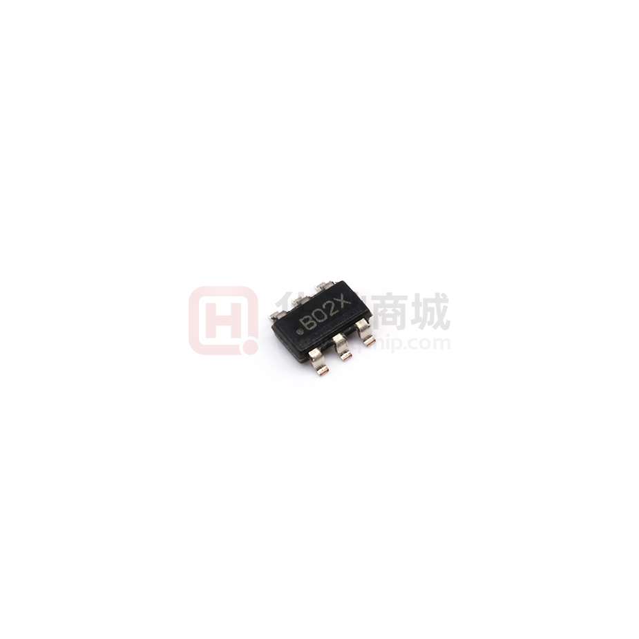
B02X
LMR14006XDDCT
ACTIVE
SOT-23-THIN
DDC
6
250
Green (RoHS
& no Sb/Br)
CU NIPDAU
Level-1-260C-UNLIM
-40 to 125
B02X
LMR14006YDDCR
ACTIVE
SOT-23-THIN
DDC
6
3000
Green (RoHS
& no Sb/Br)
CU NIPDAU
Level-1-260C-UNLIM
-40 to 125
B02Y
LMR14006YDDCT
ACTIVE
SOT-23-THIN
DDC
6
250
Green (RoHS
& no Sb/Br)
CU NIPDAU
Level-1-260C-UNLIM
-40 to 125
B02Y
(1)
The marketing status values are defined as follows:
ACTIVE: Product device recommended for new designs.
LIFEBUY: TI has announced that the device will be discontinued, and a lifetime-buy period is in effect.
NRND: Not recommended for new designs. Device is in production to support existing customers, but TI does not recommend using this part in a new design.
PREVIEW: Device has been announced but is not in production. Samples may or may not be available.
OBSOLETE: TI has discontinued the production of the device.
(2)
Eco Plan - The planned eco-friendly classification: Pb-Free (RoHS), Pb-Free (RoHS Exempt), or Green (RoHS & no Sb/Br) - please check http://www.ti.com/productcontent for the latest availability
information and additional product content details.
TBD: The Pb-Free/Green conversion plan has not been defined.
Pb-Free (RoHS): TI's terms "Lead-Free" or "Pb-Free" mean semiconductor products that are compatible with the current RoHS requirements for all 6 substances, including the requirement that
lead not exceed 0.1% by weight in homogeneous materials. Where designed to be soldered at high temperatures, TI Pb-Free products are suitable for use in specified lead-free processes.
Pb-Free (RoHS Exempt): This component has a RoHS exemption for either 1) lead-based flip-chip solder bumps used between the die and package, or 2) lead-based die adhesive used between
the die and leadframe. The component is otherwise considered Pb-Free (RoHS compatible) as defined above.
Green (RoHS & no Sb/Br): TI defines "Green" to mean Pb-Free (RoHS compatible), and free of Bromine (Br) and Antimony (Sb) based flame retardants (Br or Sb do not exceed 0.1% by weight
in homogeneous material)
(3)
MSL, Peak Temp. - The Moisture Sensitivity Level rating according to the JEDEC industry standard classifications, and peak solder temperature.
(4)
There may be additional marking, which relates to the logo, the lot trace code information, or the environmental category on the device.
(5)
Multiple Device Markings will be inside parentheses. Only one Device Marking contained in parentheses and separated by a "~" will appear on a device. If a line is indented then it is a continuation
of the previous line and the two combined represent the entire Device Marking for that device.
(6)
Lead/Ball Finish - Orderable Devices may have multiple material finish options. Finish options are separated by a vertical ruled line. Lead/Ball Finish values may wrap to two lines if the finish
value exceeds the maximum column width.
Addendum-Page 1
Samples
�PACKAGE OPTION ADDENDUM
www.ti.com
28-Feb-2017
Important Information and Disclaimer:The information provided on this page represents TI's knowledge and belief as of the date that it is provided. TI bases its knowledge and belief on information
provided by third parties, and makes no representation or warranty as to the accuracy of such information. Efforts are underway to better integrate information from third parties. TI has taken and
continues to take reasonable steps to provide representative and accurate information but may not have conducted destructive testing or chemical analysis on incoming materials and chemicals.
TI and TI suppliers consider certain information to be proprietary, and thus CAS numbers and other limited information may not be available for release.
In no event shall TI's liability arising out of such information exceed the total purchase price of the TI part(s) at issue in this document sold by TI to Customer on an annual basis.
Addendum-Page 2
�PACKAGE MATERIALS INFORMATION
www.ti.com
3-Mar-2017
TAPE AND REEL INFORMATION
*All dimensions are nominal
Device
Package Package Pins
Type Drawing
SPQ
Reel
Reel
A0
Diameter Width (mm)
(mm) W1 (mm)
B0
(mm)
K0
(mm)
P1
(mm)
LMR14006XDDCR
SOT23-THIN
DDC
6
3000
178.0
8.4
LMR14006XDDCT
SOT23-THIN
DDC
6
250
178.0
LMR14006YDDCR
SOT23-THIN
DDC
6
3000
LMR14006YDDCT
SOT23-THIN
DDC
6
250
3.2
3.2
1.4
4.0
8.0
Q3
8.4
3.2
3.2
1.4
4.0
8.0
Q3
178.0
8.4
3.2
3.2
1.4
4.0
8.0
Q3
178.0
8.4
3.2
3.2
1.4
4.0
8.0
Q3
Pack Materials-Page 1
W
Pin1
(mm) Quadrant
�PACKAGE MATERIALS INFORMATION
www.ti.com
3-Mar-2017
*All dimensions are nominal
Device
Package Type
Package Drawing
Pins
SPQ
Length (mm)
Width (mm)
Height (mm)
LMR14006XDDCR
SOT-23-THIN
DDC
6
3000
210.0
185.0
35.0
LMR14006XDDCT
SOT-23-THIN
DDC
6
250
210.0
185.0
35.0
LMR14006YDDCR
SOT-23-THIN
DDC
6
3000
210.0
185.0
35.0
LMR14006YDDCT
SOT-23-THIN
DDC
6
250
210.0
185.0
35.0
Pack Materials-Page 2
���IMPORTANT NOTICE AND DISCLAIMER
TI PROVIDES TECHNICAL AND RELIABILITY DATA (INCLUDING DATASHEETS), DESIGN RESOURCES (INCLUDING REFERENCE
DESIGNS), APPLICATION OR OTHER DESIGN ADVICE, WEB TOOLS, SAFETY INFORMATION, AND OTHER RESOURCES “AS IS”
AND WITH ALL FAULTS, AND DISCLAIMS ALL WARRANTIES, EXPRESS AND IMPLIED, INCLUDING WITHOUT LIMITATION ANY
IMPLIED WARRANTIES OF MERCHANTABILITY, FITNESS FOR A PARTICULAR PURPOSE OR NON-INFRINGEMENT OF THIRD
PARTY INTELLECTUAL PROPERTY RIGHTS.
These resources are intended for skilled developers designing with TI products. You are solely responsible for (1) selecting the appropriate
TI products for your application, (2) designing, validating and testing your application, and (3) ensuring your application meets applicable
standards, and any other safety, security, or other requirements. These resources are subject to change without notice. TI grants you
permission to use these resources only for development of an application that uses the TI products described in the resource. Other
reproduction and display of these resources is prohibited. No license is granted to any other TI intellectual property right or to any third
party intellectual property right. TI disclaims responsibility for, and you will fully indemnify TI and its representatives against, any claims,
damages, costs, losses, and liabilities arising out of your use of these resources.
TI’s products are provided subject to TI’s Terms of Sale (www.ti.com/legal/termsofsale.html) or other applicable terms available either on
ti.com or provided in conjunction with such TI products. TI’s provision of these resources does not expand or otherwise alter TI’s applicable
warranties or warranty disclaimers for TI products.
Mailing Address: Texas Instruments, Post Office Box 655303, Dallas, Texas 75265
Copyright © 2019, Texas Instruments Incorporated
�


 工商网监
湘ICP备2023018690号
工商网监
湘ICP备2023018690号
