Sample &
Buy
Product
Folder
Tools &
Software
Technical
Documents
Support &
Community
LMR16030
SNVSAH9A – DECEMBER 2015 – REVISED MAY 2016
LMR16030 SIMPLE SWITCHER® 60 V, 3 A Step-Down Converter With 40 µA IQ
1 Features
3 Description
•
•
•
•
•
•
The LMR16030 is a 60 V, 3 A SIMPLE SWITCHER®
step down regulator with an integrated high-side
MOSFET. With a wide input range from 4.3 V to 60
V, it’s suitable for various applications from industrial
to automotive for power conditioning from
unregulated sources. The regulator’s quiescent
current is 40 µA in Sleep-mode, which is suitable for
battery powered systems. An ultra-low 1 μA current in
shutdown mode can further prolong battery life. A
wide adjustable switching frequency range allows
either efficiency or external component size to be
optimized. Internal loop compensation means that the
user is free from the tedious task of loop
compensation design. This also minimizes the
external components of the device. A precision
enable input allows simplification of regulator control
and system power sequencing. The device also has
built-in protection features such as cycle-by-cycle
current limit, thermal sensing and shutdown due to
excessive power dissipation, and output overvoltage
protection.
1
•
•
•
•
•
•
•
4.3 V to 60 V Input Range
3 A Continuous Output Current
Ultra-low 40 µA Operating Quiescent Current
155 mΩ High-Side MOSFET
Current Mode Control
Adjustable Switching Frequency from 200 kHz to
2.5 MHz
Frequency Synchronization to External Clock
Internal Compensation for Ease of Use
High Duty Cycle Operation Supported
Precision Enable Input
1 µA Shutdown Current
Thermal, Overvoltage and Short Protection
8-Pin HSOIC with PowerPAD™ Package
2 Applications
•
•
•
•
Automotive Battery Regulation
Industrial Power Supplies
Telecom and Datacom Systems
General Purpose Wide Vin Regulation
space
The LMR16030 is available in an 8-pin HSOIC
package with exposed pad for low thermal resistance.
Device Information
(1)
PART NUMBER
PACKAGE
BODY SIZE (NOM)
LMR16030PDDAR
(Power Good)
HSOIC (8)
4.89 mm x 3.90 mm
HSOIC (8)
4.89 mm x 3.90 mm
LMR16030SDDAR
(Soft Start)
(1) For all available packages, see the orderable addendum at
the end of the datasheet.
Simplified Schematic
(for LMR16030S)
Efficiency vs Output Current
Vout = 5 V, fsw = 500 kHz
VIN up to 60 V
100
CIN
90
VIN
BOOT
CBOOT
RT/SYNC
80
L
D
RT
RFBT
COUT
FB
SS
CSS
GND
70
VOUT
SW
RFBB
Efficiency (%)
EN
60
50
40
30
20
VIN = 12 V
VIN = 24 V
VIN = 48 V
10
0
0.0001
0.001
0.01
0.05
IOUT (A)
0.2
0.5 1
2 3
D012
1
An IMPORTANT NOTICE at the end of this data sheet addresses availability, warranty, changes, use in safety-critical applications,
intellectual property matters and other important disclaimers. PRODUCTION DATA.
�LMR16030
SNVSAH9A – DECEMBER 2015 – REVISED MAY 2016
www.ti.com
Table of Contents
1
2
3
4
5
6
7
Features ..................................................................
Applications ...........................................................
Description .............................................................
Revision History.....................................................
Pin Configuration and Functions .........................
Specifications.........................................................
1
1
1
2
3
4
6.1
6.2
6.3
6.4
6.5
6.6
6.7
4
4
4
5
5
7
8
Absolute Maximum Ratings ......................................
ESD Ratings..............................................................
Recommended Operating Conditions ......................
Thermal Information ..................................................
Electrical Characteristics...........................................
Switching Characteristics ..........................................
Typical Characteristics ..............................................
Detailed Description ............................................ 10
7.1 Overview ................................................................. 10
7.2 Functional Block Diagram ....................................... 11
7.3 Feature Description................................................. 11
7.4 Device Functional Modes........................................ 18
8
Application and Implementation ........................ 19
8.1 Application Information............................................ 19
8.2 Typical Application ................................................. 19
9 Power Supply Recommendations...................... 24
10 Layout................................................................... 24
10.1 Layout Guidelines ................................................. 24
10.2 Layout Example .................................................... 25
11 Device and Documentation Support ................. 26
11.1
11.2
11.3
11.4
11.5
Device Support ....................................................
Community Resources..........................................
Trademarks ...........................................................
Electrostatic Discharge Caution ............................
Glossary ................................................................
26
26
26
26
26
12 Mechanical, Packaging, and Orderable
Information ........................................................... 26
4 Revision History
Changes from Original (December 2015) to Revision A
•
2
Page
Changed from Product Preview to Production Data with full version of the datasheet.......................................................... 1
Submit Documentation Feedback
Copyright © 2015–2016, Texas Instruments Incorporated
Product Folder Links: LMR16030
�LMR16030
www.ti.com
SNVSAH9A – DECEMBER 2015 – REVISED MAY 2016
5 Pin Configuration and Functions
DDA Package
8-Pin (HSOIC)
Top View
BOOT
1
VIN
2
EN
3
RT/SYNC
4
Thermal Pad
(9)
8
SW
7
GND
6
SS or PGOOD
5
FB
Pin Functions
PIN
TYPE
(1)
DESCRIPTION
NAME
NO.
BOOT
1
P
Bootstrap capacitor connection for high-side MOSFET driver. Connect a high quality 0.1 μF
capacitor from BOOT to SW.
VIN
2
P
Connect to power supply and bypass capacitors CIN. Path from VIN pin to high frequency
bypass CIN and GND must be as short as possible.
EN
3
A
Enable pin, with internal pull-up current source. Pull below 1.2 V to disable. Float or connect
to VIN to enable. Adjust the input under voltage lockout with two resistors. See the Enable
and Adjusting Under voltage lockout section.
RT/SYNC
4
A
Resistor Timing or External Clock input. An internal amplifier holds this pin at a fixed voltage
when using an external resistor to ground to set the switching frequency. If the pin is pulled
above the PLL upper threshold, a mode change occurs and the pin becomes a
synchronization input. The internal amplifier is disabled and the pin is a high impedance clock
input to the internal PLL. If clocking edges stop, the internal amplifier is re-enabled and the
operating mode returns to frequency programming by resistor.
FB
5
A
Feedback input pin, connect to the feedback divider to set VOUT. Do not short this pin to
ground during operation.
SS
or
PGOOD
6
A
SS pin for soft-start version, connect to a capacitor to set soft-start time.
PGOOD pin for Power Good version, open drain output for power-good flag, use a 10 kΩ to
100 kΩ pull-up resistor to logic rail or other DC voltage no higher than 7 V.
GND
7
G
System ground pin.
SW
8
P
Switching output of the regulator. Internally connected to high-side power MOSFET. Connect
to power inductor.
Thermal Pad
9
G
Major heat dissipation path of the die. Must be connected to ground plane on PCB.
(1)
A = Analog, P = Power, G = Ground
Submit Documentation Feedback
Copyright © 2015–2016, Texas Instruments Incorporated
Product Folder Links: LMR16030
3
�LMR16030
SNVSAH9A – DECEMBER 2015 – REVISED MAY 2016
www.ti.com
6 Specifications
6.1 Absolute Maximum Ratings
(1)
Over the recommended operating junction temperature range of -40 °C to 125 °C (unless otherwise noted)
Input Voltages
MIN
MAX
VIN, EN to GND
-0.3
65
BOOT to GND
-0.3
71
SS to GND
-0.3
5
FB to GND
-0.3
7
RT/SYNC to GND
-0.3
3.6
PGOOD to GND
-0.3
BOOT to SW
Output Voltages
UNIT
V
7
6.5
V
SW to GND
-3
65
TJ
Junction temperature
-40
150
°C
Tstg
Storage temperature
-65
150
°C
(1)
Stresses beyond those listed under Absolute Maximum Ratings may cause permanent damage to the device. These are stress ratings
only, which do not imply functional operation of the device at these or any other conditions beyond those indicated under Recommended
Operating Conditions. Exposure to absolute-maximum-rated conditions for extended periods may affect device reliability.
6.2 ESD Ratings
VALUE
V(ESD)
(1)
(2)
Electrostatic discharge
Human-body model (HBM) (1)
Charged-device model (CDM)
UNIT
±2000
(2)
V
±500
JEDEC document JEP155 states that 500-V HBM allows safe manufacturing with a standard ESD control process.
JEDEC document JEP157 states that 250-V CDM allows safe manufacturing with a standard ESD control process.
6.3 Recommended Operating Conditions
Over the recommended operating junction temperature range of -40 °C to 125 °C (unless otherwise noted)
Buck Regulator
Control
Frequency
Temperature
(1)
4
(1)
MIN
MAX
VIN
4.3
60
VOUT
0.8
50
BOOT
66
SW
-1
FB
0
5
EN
0
60
RT/SYNC
0
3.3
SS
0
3
PGOOD to GND
0
5
Switching frequency range at RT mode
200
2500
Switching frequency range at SYNC mode
250
2300
Operating junction temperature, TJ
-40
125
UNIT
V
60
V
kHz
°C
Operating Ratings indicate conditions for which the device is intended to be functional, but do not guarantee specific performance limits.
For guaranteed specifications, see Electrical Characteristics .
Submit Documentation Feedback
Copyright © 2015–2016, Texas Instruments Incorporated
Product Folder Links: LMR16030
�LMR16030
www.ti.com
SNVSAH9A – DECEMBER 2015 – REVISED MAY 2016
6.4 Thermal Information
LMR16030
THERMAL METRIC
(1) (2)
DDA (HSOIC)
UNIT
8 PINS
RθJA
Junction-to-ambient thermal resistance
42.5
°C/W
ψJT
ψJB
Junction-to-top characterization parameter
9.9
°C/W
Junction-to-board characterization parameter
25.4
°C/W
RθJC(top)
Junction-to-case (top) thermal resistance
56.1
°C/W
RθJC(bot)
Junction-to-case (bottom) thermal resistance
3.8
°C/W
RθJB
Junction-to-board thermal resistance
25.5
°C/W
(1)
(2)
For more information about traditional and new thermal metrics, see the Semiconductor and IC Package Thermal Metrics application
report, SPRA953.
Power rating at a specific ambient temperature TA should be determined with a maximum junction temperature (TJ) of 125 °C, which is
illustrated in Recommended Operating Conditions section.
6.5 Electrical Characteristics
Limits apply over the recommended operating junction temperature (TJ) range of -40 °C to +125 °C, unless otherwise stated.
Minimum and Maximum limits are specified through test, design or statistical correlation. Typical values represent the most
likely parametric norm at TJ = 25 °C, and are provided for reference purposes only. Unless otherwise specified, the following
conditions apply: VIN = 4.3 V to 60 V
PARAMETER
TEST CONDITIONS
MIN
TYP
MAX
UNIT
60
V
POWER SUPPLY (VIN PIN)
VIN
Operation input voltage
UVLO
Under voltage lockout thresholds
4.3
Rising threshold
3.8
4.0
Hysteresis
285
ISHDN
Shutdown supply current
VEN = 0 V, TA = 25 °C, 4.3 V ≤ VIN ≤ 60 V
1.0
IQ
Operating quiescent current (nonswitching)
VFB = 1.0 V, TA = 25 °C
40
4.2
V
mV
3.0
μA
μA
ENABLE (EN PIN)
VEN_TH
EN Threshold Voltage
IEN_PIN
EN PIN current
IEN_HYS
1.05
1.20
Enable threshold +50 mV
-4.6
Enable threshold -50 mV
-1.0
EN hysteresis current
1.38
V
μA
-3.6
μA
SOFT-START
ISS
SS pin current
For External Soft-Start version only, TA =
25 °C
-3.0
μA
tSS
Internal soft-start time
For Power-Good version only, 10% to
90% of FB voltage
4.0
ms
94
%
POWER GOOD (PGOOD PIN)
VPG_UV
Power-good flag under voltage tripping
threshold
POWER GOOD (% of FB voltage)
POWER BAD (% of FB voltage)
92
%
VPG_OV
Power-good flag over voltage tripping
threshold
POWER BAD (% of FB voltage)
109
%
POWER GOOD (% of FB voltage)
107
%
VPG_HYS
Power-good flag recovery hysteresis
% of FB voltage
2
IPG
PGOOD leakage current at high level
output
VPull-Up = 5 V
10
VPG_LOW
PGOOD low level output voltage
IPull-Up = 1 mA
0.1
VIN_PG_MIN
Minimum VIN for valid PGOOD output
VPull-Up < 5 V at IPull-Up = 100 μA
1.6
1.95
V
%
200
nA
V
VOLTAGE REFERENCE (FB PIN)
VFB
Feedback voltage
TJ = 25 °C
0.746
0.750
0.754
V
TJ = -40 °C to 125 °C
0.735
0.750
0.765
V
Submit Documentation Feedback
Copyright © 2015–2016, Texas Instruments Incorporated
Product Folder Links: LMR16030
5
�LMR16030
SNVSAH9A – DECEMBER 2015 – REVISED MAY 2016
www.ti.com
Electrical Characteristics (continued)
Limits apply over the recommended operating junction temperature (TJ) range of -40 °C to +125 °C, unless otherwise stated.
Minimum and Maximum limits are specified through test, design or statistical correlation. Typical values represent the most
likely parametric norm at TJ = 25 °C, and are provided for reference purposes only. Unless otherwise specified, the following
conditions apply: VIN = 4.3 V to 60 V
PARAMETER
TEST CONDITIONS
MIN
TYP
MAX
UNIT
155
320
mΩ
4.75
5.70
A
HIGH-SIDE MOSFET
RDS_ON
On-resistance
VIN = 12 V, BOOT to SW = 5.8 V
HIGH-SIDE MOSFET CURRENT LIMIT
ILIMT
Current limit
VIN = 12 V, TA = 25 °C, Open Loop
3.80
THERMAL PERFORMANCE
TSHDN
Thermal shutdown threshold
170
THYS
Hysteresis
12
6
Submit Documentation Feedback
°C
Copyright © 2015–2016, Texas Instruments Incorporated
Product Folder Links: LMR16030
�LMR16030
www.ti.com
SNVSAH9A – DECEMBER 2015 – REVISED MAY 2016
6.6 Switching Characteristics
Over the recommended operating junction temperature range of -40 °C to 125 °C (unless otherwise noted)
PARAMETER
fSW
TEST CONDITIONS
Switching frequency
RT = 11.5 kΩ
MIN
TYP
MAX
1758
1912
2066
2300
UNIT
kHz
Switching frequency range at SYNC mode
250
VSYNC_HI
SYNC clock high level threshold
1.7
VSYNC_LO
SYNC clock low level threshold
TSYNC_MIN
Minimum SYNC input pulse width
Measured at 500 kHz, VSYNC_HI > 3 V,
VSYNC_LO < 0.3 V
30
ns
TLOCK_IN
PLL lock in time
Measured at 500 kHz
100
µs
TON_MIN
Minimum controllable on time
VIN = 12 V, BOOT to SW = 5.8 V, ILoad =
1A
90
ns
DMAX
Maximum duty cycle
fSW = 200 kHz
0.5
97%
Submit Documentation Feedback
Copyright © 2015–2016, Texas Instruments Incorporated
Product Folder Links: LMR16030
V
7
�LMR16030
SNVSAH9A – DECEMBER 2015 – REVISED MAY 2016
www.ti.com
6.7 Typical Characteristics
100
100
90
90
80
80
Efficiency (%)
Efficiency (%)
Unless otherwise specified the following conditions apply: VIN = 24 V, fSW = 500 KHz, L = 8.2 µH, COUT = 2 x 47 µF, TA = 25
°C.
70
60
70
60
50
50
VIN = 12 V
VIN = 18 V
VIN = 24 V
40
30
0.001
0.01
VOUT = 3.3 V
0.1
IOUT (A)
1
VIN = 36 V
VIN = 48 V
VIN = 60 V
40
30
0.001
3
fSW = 500 KHz
VOUT = 3.3 V
100
90
90
80
80
70
60
50
1
3
D002
fSW = 500 KHz
70
60
50
VIN = 12 V
VIN = 18 V
VIN = 24 V
40
30
0.001
0.01
VOUT = 5 V
0.1
IOUT (A)
1
VIN = 36 V
VIN = 48 V
VIN = 60 V
40
30
0.001
3
0.01
0.1
IOUT (A)
D003
fSW = 500 KHz
VOUT = 5 V
Figure 3. Efficiency vs. Load Current
1
3
D004
fSW = 500 KHz
Figure 4. Efficiency vs. Load Current
125
Nominal Switching Frequency (%)
0.2
0.15
0.1
VOUT Deviation (%)
0.1
IOUT (A)
Figure 2. Efficiency vs. Load Current
100
Efficiency (%)
Efficiency (%)
Figure 1. Efficiency vs. Load Current
0.05
0
-0.05
-0.1
VIN = 12 V
VIN = 24 V
VIN = 36 V
VIN = 48 V
-0.15
-0.2
0.001
VOUT = 5 V
0.01
VFB Falling
VFB Rising
100
75
50
25
0
0.1
IOUT (A)
1
3
0
D005
0.1
0.2
0.3
0.4
VFB (V)
0.5
0.6
0.7
D005
fSW = 500 KHz
Figure 6. Frequency vs VFB
Figure 5. Load Regulation
8
0.01
D001
Submit Documentation Feedback
Copyright © 2015–2016, Texas Instruments Incorporated
Product Folder Links: LMR16030
�LMR16030
www.ti.com
SNVSAH9A – DECEMBER 2015 – REVISED MAY 2016
Typical Characteristics (continued)
Unless otherwise specified the following conditions apply: VIN = 24 V, fSW = 500 KHz, L = 8.2 µH, COUT = 2 x 47 µF, TA = 25
°C.
3.4
5.5
5
VOUT (V)
VOUT (V)
3.3
3.2
3A
2A
1A
0.5 A
0.1 A
3.1
4.1
4.2
4.3
VOUT = 3.3 V
4.4
4.5 4.6
VIN (V)
4.7
4.8
4.9
4
3A
2A
1A
0.5 A
0.1 A
3.5
3
4
4.5
3
4.5
5
5
5.5
VIN (V)
D006
fSW = 500 KHz
VOUT = 5 V
6
6.5
D007
fSW = 500 KHz
Figure 7. Dropout Curve
Figure 8. Dropout Curve
6
0.754
VIN = 12 V
VIN = 60 V
5.8
5.6
0.752
Current (A)
VFB (V)
5.4
0.75
0.748
5.2
5
4.8
4.6
4.4
0.746
4.2
0.744
-50
-25
0
25
50
75
100
Junction Temperature (qC)
125
4
-50
150
-25
0
D010
25
50
75
100
Junction Temperature (°C)
125
150
D011
VIN = 12 V
Figure 9. Voltage Reference vs Junction Temperature
Figure 10. High-Side Current Limit vs Junction Temperature
50
4
45
3.95
40
30
UVLO (V)
IQ & ISHDN (uA)
3.9
35
25
IQ
ISHDN
20
3.85
UVLO_H
UVLO_L
3.8
3.75
15
3.7
10
3.65
5
0
0
5
10
15
20
25
30 35
VIN (V)
40
45
50
55
60
3.6
-50
-25
D008
0
25
50
75
100
Junction Temperature (qC)
125
150
D009
IOUT = 0 A
Figure 11. Shut-down Current and Quiescent Current
Figure 12. UVLO Threshold
Submit Documentation Feedback
Copyright © 2015–2016, Texas Instruments Incorporated
Product Folder Links: LMR16030
9
�LMR16030
SNVSAH9A – DECEMBER 2015 – REVISED MAY 2016
www.ti.com
7 Detailed Description
7.1 Overview
The LMR16030 SIMPLE SWITCHER® regulator is an easy to use step-down DC-DC converter that operates
from a 4.3 V to 60 V supply voltage. It integrates a 155 mΩ (typical) high-side MOSFET, and is capable of
delivering up to 3 A DC load current with exceptional efficiency and thermal performance in a very small solution
size. The operating current is typically 40 μA under no load condition (not switching). When the device is
disabled, the supply current is typically 1 μA. An extended family is available in 1 A and 2 A load options in pin to
pin compatible packages.
The LMR16030 implements constant frequency peak current mode control with Sleep-mode at light load to
achieve high efficiency. The device is internally compensated, which reduces design time, and requires fewer
external components. The switching frequency is programmable from 200 kHz to 2.5 MHz by an external resistor
RT. The LMR16030 is also capable of synchronization to an external clock within the 250 kHz to 2.3 MHz
frequency range, which allows the device to be optimized to fit small board space at higher frequency, or high
efficient power conversion at lower frequency.
Other features are included for more comprehensive system requirements, including precision enable, adjustable
soft-start time, and approximate 97% duty cycle by BOOT capacitor recharge circuit. These features provide a
flexible and easy to use platform for a wide range of applications. Protection features include over temperature
shutdown, VOUT over voltage protection (OVP), VIN under-voltage lockout (UVLO), cycle-by-cycle current limit,
and short-circuit protection with frequency fold-back.
10
Submit Documentation Feedback
Copyright © 2015–2016, Texas Instruments Incorporated
Product Folder Links: LMR16030
�LMR16030
www.ti.com
SNVSAH9A – DECEMBER 2015 – REVISED MAY 2016
7.2 Functional Block Diagram
EN
PGOOD
VIN
Thermal
Shutdown
Logic
Enable
Comparator
UVLO
Shutdown
Shutdown
Logic
Enable
Threshold
UV
Voltage
Reference
Boot
Charge
OV
Boot
UVLO
Error
Amplifier
FB
PWM
Comparator
BOOT
PWM
Control
Logic
Comp
Components
Shutdown
S
Slope
Compensation
SW
Frequency
Shift
Bootstrap
Control
VIN
Oscillator
with PLL
SS
SW
Internal
Soft-Start
GND
RT/SYNC
Copyright © 2016, Texas Instruments Incorporated
7.3 Feature Description
7.3.1 Fixed Frequency Peak Current Mode Control
The following operating description of the LMR16030 will refer to the Functional Block Diagram and to the
waveforms in Figure 13. LMR16030 output voltage is regulated by turning on the high-side N-MOSFET with
controlled ON time. During high-side switch ON time, the SW pin voltage swings up to approximately VIN, and the
inductor current iL increase with linear slope (VIN – VOUT) / L. When high-side switch is off, inductor current
discharges through freewheel diode with a slope of –VOUT / L. The control parameter of Buck converter is defined
as Duty Cycle D = tON / TSW, where tON is the high-side switch ON time and TSW is the switching period. The
regulator control loop maintains a constant output voltage by adjusting the duty cycle D. In an ideal Buck
converter, where losses are ignored, D is proportional to the output voltage and inversely proportional to the input
voltage: D = VOUT / VIN.
Submit Documentation Feedback
Copyright © 2015–2016, Texas Instruments Incorporated
Product Folder Links: LMR16030
11
�LMR16030
SNVSAH9A – DECEMBER 2015 – REVISED MAY 2016
www.ti.com
Feature Description (continued)
VSW
SW Voltage
D = tON/ TSW
VIN
tON
tOFF
t
0
-VD
Inductor Current
iL
TSW
ILPK
IOUT
ûiL
t
0
Figure 13. SW Node and Inductor Current Waveforms in
Continuous Conduction Mode (CCM)
The LMR16030 employs fixed frequency peak current mode control. A voltage feedback loop is used to get
accurate DC voltage regulation by adjusting the peak current command based on voltage offset. The peak
inductor current is sensed from the high-side switch and compared to the peak current to control the ON time of
the high-side switch. The voltage feedback loop is internally compensated, which allows for fewer external
components, makes it easy to design, and provides stable operation with almost any combination of output
capacitors. The regulator operates with fixed switching frequency at normal load condition. At very light load, the
LMR16030 will operate in Sleep-mode to maintain high efficiency and the switching frequency will decrease with
reduced load current.
7.3.2 Slope Compensation
The LMR16030 adds a compensating ramp to the MOSFET switch current sense signal. This slope
compensation prevents sub-harmonic oscillations at duty cycles greater than 50%. The peak current limit of the
high-side switch is not affected by the slope compensation and remains constant over the full duty cycle range.
7.3.3 Sleep-mode
The LMR16030 operates in Sleep-mode at light load currents to improve efficiency by reducing switching and
gate drive losses. If the output voltage is within regulation and the peak switch current at the end of any
switching cycle is below the current threshold of 300 mA, the device enters Sleep-mode. The Sleep-mode current
threshold is the peak switch current level corresponding to a nominal internal COMP voltage of 400 mV.
When in Sleep-mode, the internal COMP voltage is clamped at 400 mV and the high-side MOSFET is inhibited,
and the device draws only 40 μA (typical) input quiescent current. Since the device is not switching, the output
voltage begins to decay. The voltage control loop responds to the falling output voltage by increasing the internal
COMP voltage. The high-side MOSFET is enabled and switching resumes when the error amplifier lifts internal
COMP voltage above 400 mV. The output voltage recovers to the regulated value, and internal COMP voltage
eventually falls below the Sleep-mode threshold at which time the device again enters Sleep-mode.
7.3.4 Low Dropout Operation and Bootstrap Voltage (BOOT)
The LMR16030 provides an integrated bootstrap voltage regulator. A small capacitor between the BOOT and
SW pins provides the gate drive voltage for the high-side MOSFET. The BOOT capacitor is refreshed when the
high-side MOSFET is off and the external low side diode conducts. The recommended value of the BOOT
capacitor is 0.1 μF. A ceramic capacitor with an X7R or X5R grade dielectric with a voltage rating of 16 V or
greater is recommended for stable performance over temperature and voltage.
12
Submit Documentation Feedback
Copyright © 2015–2016, Texas Instruments Incorporated
Product Folder Links: LMR16030
�LMR16030
www.ti.com
SNVSAH9A – DECEMBER 2015 – REVISED MAY 2016
Feature Description (continued)
When operating with a low voltage difference from input to output, the high-side MOSFET of the LMR16030 will
operate at approximate 97% duty cycle. When the high-side MOSFET is continuously on for 5 or 6 switching
cycles (5 or 6 switching cycles for frequency lower than 1 MHz, and 10 or 11 switching cycles for frequency
higher than 1 MHz) and the voltage from BOOT to SW drops below 3.2 V, the high-side MOSFET is turned off
and an integrated low side MOSFET pulls SW low to recharge the BOOT capacitor.
Since the gate drive current sourced from the BOOT capacitor is small, the high-side MOSFET can remain on for
many switching cycles before the MOSFET is turned off to refresh the capacitor. Thus the effective duty cycle of
the switching regulator can be high, approaching 97%. The effective duty cycle of the converter during dropout is
mainly influenced by the voltage drops across the power MOSFET, the inductor resistance, the low side diode
voltage and the printed circuit board resistance.
7.3.5 Adjustable Output Voltage
The internal voltage reference produces a precise 0.75 V (typical) voltage reference over the operating
temperature range. The output voltage is set by a resistor divider from output voltage to the FB pin. It is
recommended to use 1% tolerance or better and temperature coefficient of 100 ppm or less divider resistors.
Select the low side resistor RFBB for the desired divider current and use Equation 1 to calculate high-side RFBT.
Larger value divider resistors are good for efficiency at light load. However, if the values are too high, the
regulator will be more susceptible to noise and voltage errors from the FB input current may become noticeable.
RFBB in the range from 10 kΩ to 100 kΩ is recommended for most applications.
VOUT
RFBT
FB
RFBB
Figure 14. Output Voltage Setting
RFBT
VOUT 0.75
u RFBB
0.75
(1)
7.3.6 Enable and Adjustable Under-voltage Lockout
The LMR16030 is enabled when the VIN pin voltage rises above 4.0 V (typical) and the EN pin voltage exceeds
the enable threshold of 1.2 V (typical). The LMR16030 is disabled when the VIN pin voltage falls below 3.715 V
(typical) or when the EN pin voltage is below 1.2 V. The EN pin has an internal pull-up current source (typically
IEN = 1 μA) that enables operation of the LMR16030 when the EN pin is floating.
Many applications will benefit from the employment of an enable divider RENT and RENB in Figure 15 to establish
a precision system UVLO level for the stage. System UVLO can be used for supplies operating from utility power
as well as battery power. It can be used for sequencing, ensuring reliable operation, or supply protection, such
as a battery. An external logic signal can also be used to drive EN input for system sequencing and protection.
When EN terminal voltage exceeds 1.2 V, an additional hysteresis current (typically IHYS = 3.6 μA) is sourced out
of EN terminal. When the EN terminal is pulled below 1.2 V, IHYS current is removed. This additional current
facilitates adjustable input voltage UVLO hysteresis. Use Equation 2 and Equation 3 to calculate RENT and RENB
for desired UVLO hysteresis voltage.
Submit Documentation Feedback
Copyright © 2015–2016, Texas Instruments Incorporated
Product Folder Links: LMR16030
13
�LMR16030
SNVSAH9A – DECEMBER 2015 – REVISED MAY 2016
www.ti.com
Feature Description (continued)
IEN_HYS
IEN
VIN
VIN
RENT
VEN
EN
RENB
Figure 15. System UVLO By Enable Dividers
RENT
RENB
VSTART VSTOP
IHYS
VEN
VSTART VEN
RENT
(2)
IEN
(3)
where VSTART is the desired voltage threshold to enable LMR16030, VSTOP is the desired voltage threshold to
disable device, IEN = 1 μA and IHYS = 3.6 μA typically.
7.3.7 External Soft-start
The LMR16030S has external soft-start pin for programmable output ramp up time. The soft-start feature is used
to prevent inrush current impacting the LMR16030 and its load when power is first applied. The soft-start time
can be programed by connecting an external capacitor CSS from SS pin to GND. An internal current source
(typically ISS = 3 μA) charges CSS and generates a ramp from 0 V to VREF. The soft-start time can be calculated
by Equation 4:
CSS (nF) u VREF (V)
tSS (ms)
ISS (PA)
(4)
The internal soft-start resets while device is disabled or in thermal shutdown.
7.3.8 Switching Frequency and Synchronization (RT/SYNC)
The switching frequency of the LMR16030 can be programmed by the resistor RT from the RT/SYNC pin and
GND pin. The RT/SYNC pin can’t be left floating or shorted to ground. To determine the timing resistance for a
given switching frequency, use Equation 5 or the curve in Figure 16. Table 1 gives typical RT values for a given
fSW.
RT (k:)
14
42904 u ¦SW N+]
1.088
(5)
Submit Documentation Feedback
Copyright © 2015–2016, Texas Instruments Incorporated
Product Folder Links: LMR16030
�LMR16030
www.ti.com
SNVSAH9A – DECEMBER 2015 – REVISED MAY 2016
Feature Description (continued)
140
120
RT (k:)
100
80
60
40
20
0
0
500
1000
1500
Frequency (kHz)
2000
2500
D008
Figure 16. RT vs Frequency Curve
Table 1. Typical Frequency Setting RT Resistance
fSW (kHz)
RT (kΩ)
200
133
350
73.2
500
49.9
750
32.4
1000
23.2
1500
15.0
1912
11.5
2200
9.76
The LMR16030 switching action can also be synchronized to an external clock from 250 kHz to 2.3 MHz.
Connect a square wave to the RT/SYNC pin through either circuit network shown in Figure 17. Internal oscillator
is synchronized by the falling edge of external clock. The recommendations for the external clock include: high
level no lower than 1.7 V, low level no higher than 0.5 V and have a pulse width greater than 30 ns. When using
a low impedance signal source, the frequency setting resistor RT is connected in parallel with an AC coupling
capacitor CCOUP to a termination resistor RTERM (e.g., 50 Ω). The two resistors in series provide the default
frequency setting resistance when the signal source is turned off. A 10 pF ceramic capacitor can be used for
CCOUP. Figure 18, Figure 19 and Figure 20 show the device synchronized to an external system clock.
CCOUP
PLL
PLL
Lo-Z
Clock
Source
RT
RT/SYNC
RTERM
Hi-Z
Clock
Source
RT/SYNC
RT
Figure 17. Synchronizing to an External Clock
Submit Documentation Feedback
Copyright © 2015–2016, Texas Instruments Incorporated
Product Folder Links: LMR16030
15
�LMR16030
SNVSAH9A – DECEMBER 2015 – REVISED MAY 2016
www.ti.com
Figure 18. Synchronizing in CCM
Figure 19. Synchronizing in DCM
Figure 20. Synchronizing in Sleep-mode Mode
Equation 6 calculates the maximum switching frequency limitation set by the minimum controllable on time and
the input to output step down ratio. Setting the switching frequency above this value will cause the regulator to
skip switching pulses to achieve the low duty cycle required at maximum input voltage.
¦SW(max)
§ IOUT u RIND VOUT VD ·
u¨
¸
tON ¨© VIN_MAX IOUT u RDS_ON VD ¸¹
1
(6)
where
• IOUT = Output current
• RIND = Inductor series resistance
• VIN_MAX = Maximum input voltage
• VOUT = Output voltage
• VD = Diode voltage drop
• RDS_ON = High-side MOSFET switch on resistance
• tON = Minimum on time
7.3.9 Power Good (PGOOD)
The LMR16030P has a built in power-good flag shown on PGOOD pin to indicate whether the output voltage is
within its regulation level. The PGOOD signal can be used for start-up sequencing of multiple rails or fault
protection. The PGOOD pin is an open-drain output that requires a pull-up resistor to an appropriate DC voltage.
Voltage seen by the PGOOD pin should never exceed 7 V. A resistor divider pair can be used to divide the
voltage down from a higher potential. A typical range of pull-up resistor value is 10 kΩ to 100 kΩ.
Refer to Figure 21. When the FB voltage is within the power-good band, +7% above and -6% below the internal
reference VREF typically, the PGOOD switch will be turned off and the PGOOD voltage will be pulled up to the
voltage level defined by the pull-up resistor or divider. When the FB voltage is outside of the tolerance band,
+9% above or -8% below VREF typically, the PGOOD switch will be turned on and the PGOOD pin voltage will be
pulled low to indicate power bad.
16
Submit Documentation Feedback
Copyright © 2015–2016, Texas Instruments Incorporated
Product Folder Links: LMR16030
�LMR16030
www.ti.com
SNVSAH9A – DECEMBER 2015 – REVISED MAY 2016
VREF
109%
107%
94%
92%
PGOOD
High
Low
Figure 21. Power-Good Flag
7.3.10 Over Current and Short Circuit Protection
The LMR16030 is protected from over current condition by cycle-by-cycle current limiting on the peak current of
the high-side MOSFET. High-side MOSFET over-current protection is implemented by the nature of the Peak
Current Mode control. The high-side switch current is compared to the output of the Error Amplifier (EA) minus
slope compensation every switching cycle. Please refer to Functional Block Diagram for more details. The peak
current of high-side switch is limited by a clamped maximum peak current threshold which is constant. So the
peak current limit of the high-side switch is not affected by the slope compensation and remains constant over
the full duty cycle range.
The LMR16030 also implements a frequency fold-back to protect the converter in severe over-current or short
conditions. The oscillator frequency is divided by 2, 4, and 8 as the FB pin voltage decrease to 75%, 50%, 25%
of VREF. The frequency fold-back increases the off time by increasing the period of the switching cycle, so that it
provides more time for the inductor current to ramp down and leads to a lower average inductor current. Lower
frequency also means lower switching loss. Frequency fold-back reduces power dissipation and prevents
overheating and potential damage to the device.
7.3.11 Overvoltage Protection
The LMR16030 employs an output overvoltage protection (OVP) circuit to minimize voltage overshoot when
recovering from output fault conditions or strong unload transients in designs with low output capacitance. The
OVP feature minimizes output overshoot by turning off high-side switch immediately when FB voltage reaches to
the rising OVP threshold which is nominally 109% of the internal voltage reference VREF. When the FB voltage
drops below the falling OVP threshold which is nominally 107% of VREF, the high-side MOSFET resumes normal
operation.
7.3.12 Thermal Shutdown
The LMR16030 provides an internal thermal shutdown to protect the device when the junction temperature
exceeds 170 °C (typical). The high-side MOSFET stops switching when thermal shundown activates. Once the
die temperature falls below 158 °C (typical), the device reinitiates the power up sequence controlled by the
internal soft-start circuitry.
Submit Documentation Feedback
Copyright © 2015–2016, Texas Instruments Incorporated
Product Folder Links: LMR16030
17
�LMR16030
SNVSAH9A – DECEMBER 2015 – REVISED MAY 2016
www.ti.com
7.4 Device Functional Modes
7.4.1 Shutdown Mode
The EN pin provides electrical ON and OFF control for the LMR16030. When VEN is below 1.0 V, the device is in
shutdown mode. The switching regulator is turned off and the quiescent current drops to 1.0 µA typically. The
LMR16030 also employs under voltage lock out protection. If VIN voltage is below the UVLO level, the regulator
will be turned off.
7.4.2 Active Mode
The LMR16030 is in Active Mode when VEN is above the precision enable threshold and VIN is above its UVLO
level. The simplest way to enable the LMR16030 is to connect the EN pin to VIN pin. This allows self startup
when the input voltage is in the operation range: 4.3 V to 60 V. Please refer to Enable and Adjustable Undervoltage Lockout for details on setting these operating levels.
In Active Mode, depending on the load current, the LMR16030 will be in one of three modes:
1. Continuous conduction mode (CCM) with fixed switching frequency when load current is above half of the
peak-to-peak inductor current ripple.
2. Discontinuous conduction mode (DCM) with fixed switching frequency when load current is lower than half of
the peak-to-peak inductor current ripple in CCM operation.
3. Sleep-mode when internal COMP voltage drop to 400 mV at very light load.
7.4.3 CCM Mode
CCM operation is employed in the LMR16030 when the load current is higher than half of the peak-to-peak
inductor current. In CCM operation, the frequency of operation is fixed, output voltage ripple will be at a minimum
in this mode and the maximum output current of 3 A can be supplied by the LMR16030.
7.4.4 Light Load Operation
When the load current is lower than half of the peak-to-peak inductor current in CCM, the LMR16030 will operate
in DCM. At even lighter current loads, Sleep-mode is activated to maintain high efficiency operation by reducing
switching and gate drive losses.
18
Submit Documentation Feedback
Copyright © 2015–2016, Texas Instruments Incorporated
Product Folder Links: LMR16030
�LMR16030
www.ti.com
SNVSAH9A – DECEMBER 2015 – REVISED MAY 2016
8 Application and Implementation
NOTE
Information in the following applications sections is not part of the TI component
specification, and TI does not warrant its accuracy or completeness. TI’s customers are
responsible for determining suitability of components for their purposes. Customers should
validate and test their design implementation to confirm system functionality.
8.1 Application Information
The LMR16030 is a step down DC-to-DC regulator. It is typically used to convert a higher DC voltage to a lower
DC voltage with a maximum output current of 3 A. The following design procedure can be used to select
components for the LMR16030. This section presents a simplified discussion of the design process.
8.2 Typical Application
The LMR16030 only requires a few external components to convert from wide voltage range supply to a fixed
output voltage. A schematic of 5 V / 3 A application circuit is shown in Figure 22. The external components have
to fulfill the needs of the application, but also the stability criteria of the device’s control loop.
7 V to 60 V
CBOOT
VIN
CIN
EN
BOOT
L
SW
5V/3A
COUT
D
RFBT
RT/SYNC
FB
RFBB
RT
SS
GND
CSS
Figure 22. Application Circuit, 5V Output
8.2.1 Design Requirements
This example details the design of a high frequency switching regulator using ceramic output capacitors. A few
parameters must be known in order to start the design process. These parameters are typically determined at the
system level:
Table 2. Design Parameters
Input Voltage, VIN
7 V to 60 V, Typical 24 V
Output Voltage, VOUT
5.0 V
Maximum Output Current IO_MAX
3A
Transient Response 0.3 A to 3 A
5%
Output Voltage Ripple
50 mV
Input Voltage Ripple
400 mV
Switching Frequency fSW
500 KHz
Submit Documentation Feedback
Copyright © 2015–2016, Texas Instruments Incorporated
Product Folder Links: LMR16030
19
�LMR16030
SNVSAH9A – DECEMBER 2015 – REVISED MAY 2016
www.ti.com
8.2.2 Detailed Design Procedure
8.2.2.1
Output Voltage Set-Point
The output voltage of LMR16030 is externally adjustable using a resistor divider network. The divider network is
comprised of top feedback resistor RFBT and bottom feedback resistor RFBB. Equation 7 is used to determine the
output voltage:
VOUT 0.75
RFBT
u RFBB
0.75
(7)
Choose the value of RFBT to be 100 kΩ. With the desired output voltage set to 5 V and the VFB = 0.75 V, the RFBB
value can then be calculated using Equation 7. The formula yields to a value 17.65 kΩ. Choose the closest
available value of 17.8 kΩ for RFBB.
8.2.2.2
Switching Frequency
For desired frequency, use Equation 8 to calculate the required value for RT.
RT (k:)
42904 u ¦SW N+]
1.088
(8)
For 500 KHz, the calculated RT is 49.66 kΩ and standard value 49.9 kΩ can be used to set the switching
frequency at 500 KHz.
8.2.2.3
Output Inductor Selection
The most critical parameters for the inductor are the inductance, saturation current and the RMS current. The
inductance is based on the desired peak-to-peak ripple current ΔiL. Since the ripple current increases with the
input voltage, the maximum input voltage is always used to calculate the minimum inductance LMIN. Use
Equation 9 to calculate the minimum value of the output inductor. KIND is a coefficient that represents the amount
of inductor ripple current relative to the maximum output current. A reasonable value of KIND should be 20%-40%.
During an instantaneous short or over current operation event, the RMS and peak inductor current can be high.
The inductor current rating should be higher than current limit.
VOUT u (VIN_MAX VOUT )
'iL
VIN _ MAX u L u ¦SW
(9)
LMIN
VIN_MAX
VOUT
IOUT u KIND
u
VOUT
VIN_MAX u ¦SW
(10)
In general, it is preferable to choose lower inductance in switching power supplies, because it usually
corresponds to faster transient response, smaller DCR, and reduced size for more compact designs. But too low
of an inductance can generate too large of an inductor current ripple such that over current protection at the full
load could be falsely triggered. It also generates more conduction loss since the RMS current is slightly higher.
Larger inductor current ripple also implies larger output voltage ripple with same output capacitors. With peak
current mode control, it is not recommended to have too small of an inductor current ripple. A larger peak current
ripple improves the comparator signal to noise ratio.
For this design example, choose KIND = 0.4, the minimum inductor value is calculated to be 7.64 µH, and a
nearest standard value is chosen: 8.2 µH. A standard 8.2 μH ferrite inductor with a capability of 3 A RMS current
and 6 A saturation current can be used.
8.2.2.4
Output Capacitor Selection
The output capacitor(s), COUT, should be chosen with care since it directly affects the steady state output voltage
ripple, loop stability and the voltage over/undershoot during load current transients.
The output ripple is essentially composed of two parts. One is caused by the inductor current ripple going
through the Equivalent Series Resistance (ESR) of the output capacitors:
'VOUT_ESR 'iL u ESR KIND u IOUT u ESR
(11)
The other is caused by the inductor current ripple charging and discharging the output capacitors:
KIND u IOUT
'iL
'VOUT_C
8 u ¦SW u COUT 8 u ¦SW u COUT
20
Submit Documentation Feedback
(12)
Copyright © 2015–2016, Texas Instruments Incorporated
Product Folder Links: LMR16030
�LMR16030
www.ti.com
SNVSAH9A – DECEMBER 2015 – REVISED MAY 2016
The two components in the voltage ripple are not in phase, so the actual peak-to-peak ripple is smaller than the
sum of two peaks.
Output capacitance is usually limited by transient performance specifications if the system requires tight voltage
regulation with presence of large current steps and fast slew rate. When a fast large load increase happens,
output capacitors provide the required charge before the inductor current can slew up to the appropriate level.
The regulator’s control loop usually needs three or more clock cycles to respond to the output voltage droop. The
output capacitance must be large enough to supply the current difference for three clock cycles to maintain the
output voltage within the specified range. Equation 13 shows the minimum output capacitance needed for
specified output undershoot. When a sudden large load decrease happens, the output capacitors absorb energy
stored in the inductor. The catch diode can’t sink current so the energy stored in the inductor results in an output
voltage overshoot. Equation 14 calculates the minimum capacitance required to keep the voltage overshoot
within a specified range.
3 u (IOH IOL )
COUT !
¦SW u 9US
(13)
COUT !
2
2
IOH
IOL
(VOUT
VOS )2
2
VOUT
uL
(14)
where
• KIND = Ripple ratio of the inductor ripple current (ΔiL / IOUT)
• IOL = Low level output current during load transient
• IOH = High level output current during load transient
• VUS = Target output voltage undershoot
• VOS = Target output voltage overshoot
For this design example, the target output ripple is 50 mV. Presuppose ΔVOUT_ESR = ΔVOUT_C = 50 mV, and
chose KIND = 0.4. Equation 11 yields ESR no larger than 41.7 mΩ and Equation 12 yields COUT no smaller than 6
μF. For the target over/undershoot range of this design, VUS = VOS = 5% × VOUT = 250 mV. The COUT can be
calculated to be no smaller than 64.8 μF and 6.4 μF by Equation 13 and Equation 14 respectively. In summary,
the most stringent criteria for the output capacitor is 100 μF. For this design example, two 47 μF, 16 V, X7R
ceramic capacitors with 5 mΩ ESR are used in parallel.
8.2.2.5
Schottky Diode Selection
The breakdown voltage rating of the diode is preferred to be 25% higher than the maximum input voltage. The
current rating for the diode should be equal to the maximum output current for best reliability in most
applications. In cases where the input voltage is much greater than the output voltage the average diode current
is lower. In this case it is possible to use a diode with a lower average current rating, approximately (1-D) × IOUT
however the peak current rating should be higher than the maximum load current. A 3 A rated diode is a good
starting point.
8.2.2.6
Input Capacitor Selection
The LMR16030 device requires high frequency input decoupling capacitor(s) and a bulk input capacitor,
depending on the application. The typical recommended value for the high frequency decoupling capacitor is 4.7
μF to 10 μF. A high-quality ceramic capacitor type X5R or X7R with sufficiency voltage rating is recommended.
To compensate the derating of ceramic capacitors, a voltage rating of twice the maximum input voltage is
recommended. Additionally, some bulk capacitance can be required, especially if the LMR16030 circuit is not
located within approximately 5 cm from the input voltage source. This capacitor is used to provide damping to the
voltage spike due to the lead inductance of the cable or the trace. For this design, two 2.2 μF, X7R ceramic
capacitors rated for 100 V are used. A 0.1 μF for high-frequency filtering and place it as close as possible to the
device pins.
8.2.2.7
Bootstrap Capacitor Selection
Every LMR16030 design requires a bootstrap capacitor (CBOOT). The recommended capacitor is 0.1 μF and rated
16 V or higher. The bootstrap capacitor is located between the SW pin and the BOOT pin. The bootstrap
capacitor must be a high-quality ceramic type with an X7R or X5R grade dielectric for temperature stability.
Submit Documentation Feedback
Copyright © 2015–2016, Texas Instruments Incorporated
Product Folder Links: LMR16030
21
�LMR16030
SNVSAH9A – DECEMBER 2015 – REVISED MAY 2016
www.ti.com
8.2.3 Application Curves
Unless otherwise specified the following conditions apply: VIN = 24 V, fSW = 500 KHz, L = 8.2 µH, COUT = 2 x 47 µF, TA = 25
°C.
VIN = 24 V
VOUT = 5 V
IOUT = 2 A
VIN = 24 V
VOUT = 5 V
IOUT = 0 A
VIN = 24 V
Figure 25. Sleep-mode
VIN = 24 V
VOUT = 5 V
IOUT = 2 A
Figure 24. Start-up By VIN
Figure 23. Start-up By EN
VIN = 24 V
VOUT = 5 V
VOUT = 5 V
IOUT = 200 mA
Figure 26. DCM Mode
IOUT = 2 A
IOUT: 20% → 80%
of 3 A
Slew rate = 100
mA/μs
Figure 27. CCM Mode
Figure 28. Load Transient
22
Submit Documentation Feedback
Copyright © 2015–2016, Texas Instruments Incorporated
Product Folder Links: LMR16030
�LMR16030
www.ti.com
SNVSAH9A – DECEMBER 2015 – REVISED MAY 2016
Unless otherwise specified the following conditions apply: VIN = 24 V, fSW = 500 KHz, L = 8.2 µH, COUT = 2 x 47 µF, TA = 25
°C.
VIN = 24 V
VOUT = 5 V
VIN = 24 V
Figure 29. Output Short
VOUT = 5 V
Figure 30. Output Short Recovery
Submit Documentation Feedback
Copyright © 2015–2016, Texas Instruments Incorporated
Product Folder Links: LMR16030
23
�LMR16030
SNVSAH9A – DECEMBER 2015 – REVISED MAY 2016
www.ti.com
9 Power Supply Recommendations
The LMR16030 is designed to operate from an input voltage supply range between 4.3 V and 60 V. This input
supply should be able to withstand the maximum input current and maintain a stable voltage. The resistance of
the input supply rail should be low enough that an input current transient does not cause a high enough drop at
the LMR16030 supply voltage that can cause a false UVLO fault triggering and system reset. If the input supply
is located more than a few inches from the LMR16030, additional bulk capacitance may be required in addition to
the ceramic input capacitors. The amount of bulk capacitance is not critical, but a 47 μF or 100 μF electrolytic
capacitor is a typical choice .
10 Layout
10.1 Layout Guidelines
Layout is a critical portion of good power supply design. The following guidelines will help users design a PCB
with the best power conversion performance, thermal performance, and minimized generation of unwanted EMI.
1. The feedback network, resistor RFBT and RFBB, should be kept close to the FB pin. VOUT sense path away
from noisy nodes and preferably through a layer on the other side of a shielding layer.
2. The input bypass capacitor CIN must be placed as close as possible to the VIN pin and ground. Grounding
for both the input and output capacitors should consist of localized top side planes that connect to the GND
pin and PAD.
3. The inductor L should be placed close to the SW pin to reduce magnetic and electrostatic noise.
4. The output capacitor, COUT should be placed close to the junction of L and the diode D. The L, D, and COUT
trace should be as short as possible to reduce conducted and radiated noise and increase overall efficiency.
5. The ground connection for the diode, CIN, and COUT should be as small as possible and tied to the system
ground plane in only one spot (preferably at the COUT ground point) to minimize conducted noise in the
system ground plane.
6. For more detail on switching power supply layout considerations see SNVA021 Application Note AN-1149.
24
Submit Documentation Feedback
Copyright © 2015–2016, Texas Instruments Incorporated
Product Folder Links: LMR16030
�LMR16030
www.ti.com
SNVSAH9A – DECEMBER 2015 – REVISED MAY 2016
10.2 Layout Example
Output Bypass
Capacitor
Output
Inductor
Rectifier Diode
BOOT
Capacitor
Input Bypass
Capacitor
BOOT
UVLO Adjust
Resistor
SW
VIN
GND
EN
SS
RT/SYNC
FB
Soft-Start
Capacitor
Output Voltage
Set Resistor
Frequency
Set Resistor
Thermal VIA
Signal VIA
Figure 31. Layout
Submit Documentation Feedback
Copyright © 2015–2016, Texas Instruments Incorporated
Product Folder Links: LMR16030
25
�LMR16030
SNVSAH9A – DECEMBER 2015 – REVISED MAY 2016
www.ti.com
11 Device and Documentation Support
11.1 Device Support
11.1.1 Third-Party Products Disclaimer
TI'S PUBLICATION OF INFORMATION REGARDING THIRD-PARTY PRODUCTS OR SERVICES DOES NOT
CONSTITUTE AN ENDORSEMENT REGARDING THE SUITABILITY OF SUCH PRODUCTS OR SERVICES
OR A WARRANTY, REPRESENTATION OR ENDORSEMENT OF SUCH PRODUCTS OR SERVICES, EITHER
ALONE OR IN COMBINATION WITH ANY TI PRODUCT OR SERVICE.
11.2 Community Resources
The following links connect to TI community resources. Linked contents are provided "AS IS" by the respective
contributors. They do not constitute TI specifications and do not necessarily reflect TI's views; see TI's Terms of
Use.
TI E2E™ Online Community TI's Engineer-to-Engineer (E2E) Community. Created to foster collaboration
among engineers. At e2e.ti.com, you can ask questions, share knowledge, explore ideas and help
solve problems with fellow engineers.
Design Support TI's Design Support Quickly find helpful E2E forums along with design support tools and
contact information for technical support.
11.3 Trademarks
PowerPAD, E2E are trademarks of Texas Instruments.
SIMPLE SWITCHER is a registered trademark of Texas Instruments.
All other trademarks are the property of their respective owners.
11.4 Electrostatic Discharge Caution
These devices have limited built-in ESD protection. The leads should be shorted together or the device placed in conductive foam
during storage or handling to prevent electrostatic damage to the MOS gates.
11.5 Glossary
SLYZ022 — TI Glossary.
This glossary lists and explains terms, acronyms, and definitions.
12 Mechanical, Packaging, and Orderable Information
The following pages include mechanical, packaging, and orderable information. This information is the most
current data available for the designated devices. This data is subject to change without notice and revision of
this document. For browser-based versions of this data sheet, refer to the left-hand navigation.
26
Submit Documentation Feedback
Copyright © 2015–2016, Texas Instruments Incorporated
Product Folder Links: LMR16030
�LMR16030
www.ti.com
SNVSAH9A – DECEMBER 2015 – REVISED MAY 2016
Submit Documentation Feedback
Copyright © 2015–2016, Texas Instruments Incorporated
Product Folder Links: LMR16030
27
�PACKAGE OPTION ADDENDUM
www.ti.com
6-Feb-2020
PACKAGING INFORMATION
Orderable Device
Status
(1)
Package Type Package Pins Package
Drawing
Qty
Eco Plan
Lead/Ball Finish
MSL Peak Temp
(2)
(6)
(3)
Op Temp (°C)
Device Marking
(4/5)
LMR16030PDDA
ACTIVE SO PowerPAD
DDA
8
75
Green (RoHS
& no Sb/Br)
NIPDAUAG
Level-2-260C-1 YEAR
-40 to 125
SB3P
LMR16030PDDAR
ACTIVE SO PowerPAD
DDA
8
2500
Green (RoHS
& no Sb/Br)
NIPDAUAG
Level-2-260C-1 YEAR
-40 to 125
SB3P
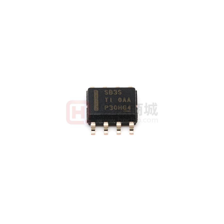
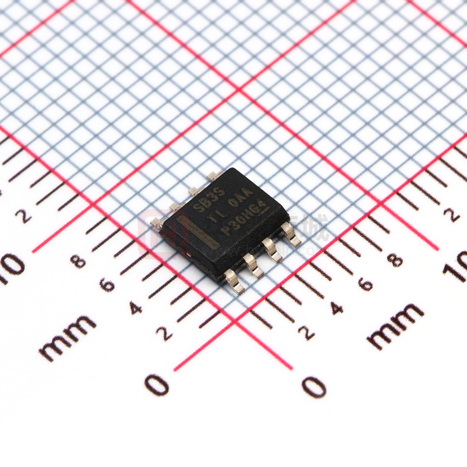
LMR16030SDDA
ACTIVE SO PowerPAD
DDA
8
75
Green (RoHS
& no Sb/Br)
NIPDAUAG
Level-2-260C-1 YEAR
-40 to 125
SB3S
LMR16030SDDAR
ACTIVE SO PowerPAD
DDA
8
2500
Green (RoHS
& no Sb/Br)
NIPDAUAG
Level-2-260C-1 YEAR
-40 to 125
SB3S
(1)
The marketing status values are defined as follows:
ACTIVE: Product device recommended for new designs.
LIFEBUY: TI has announced that the device will be discontinued, and a lifetime-buy period is in effect.
NRND: Not recommended for new designs. Device is in production to support existing customers, but TI does not recommend using this part in a new design.
PREVIEW: Device has been announced but is not in production. Samples may or may not be available.
OBSOLETE: TI has discontinued the production of the device.
(2)
RoHS: TI defines "RoHS" to mean semiconductor products that are compliant with the current EU RoHS requirements for all 10 RoHS substances, including the requirement that RoHS substance
do not exceed 0.1% by weight in homogeneous materials. Where designed to be soldered at high temperatures, "RoHS" products are suitable for use in specified lead-free processes. TI may
reference these types of products as "Pb-Free".
RoHS Exempt: TI defines "RoHS Exempt" to mean products that contain lead but are compliant with EU RoHS pursuant to a specific EU RoHS exemption.
Green: TI defines "Green" to mean the content of Chlorine (Cl) and Bromine (Br) based flame retardants meet JS709B low halogen requirements of


 工商网监
湘ICP备2023018690号
工商网监
湘ICP备2023018690号
