User's Guide
SNVA505A – September 2011 – Revised April 2013
AN-2193 LMR24220 Multi-Rail Reference Board
1
Introduction
The LMR24220 multi-rail reference board implements an extremely compact solution. It is designed to
convert from 12 V or 24 V rails down to typical point-of-load voltages of 3.3V, 1.8V and 1.2V. This design
utilizes an LMR24220 Nano Regulator and two LMZ10501 Nano Modules to demonstrate a complete
solution for space constrained multi-rail applications.
The complete solution size is 20.32 x 13.34 x 2mm with all components placed on a single side. The
board can be plugged into a standard 8-pin header with 100 mil spacing and total thickness less than 100
mils for ease of prototyping.
2
Features
•
•
•
•
•
3
5 V to 32 V Input Voltage Range
3.3 V / 1.8 V / 1.2 V Output Voltage Rails
Up to 1000 mA Output Current Per Rail
Small Solution Size (20.32 x 13.34 x 2mm)
No External Compensation Required
Shutdown Operation
The reference board includes a resistor divider that implements an under voltage lockout (UVLO) that
disables the part when VIN is below 4 V. The threshold for the UVLO can be adjusted to suit the needs of
the application.
Ret = (VUVLO* 10K - 12.4K)
(1)
The midpoint of the resistor divider is clamped to 4.3 V by diode D2 so that the EN pin voltage of the
LMR24220 does not exceed 7V. The midpoint is also tied to pin 8 of the header (EN). Use the EN pin to
disable the device by pulling this node to GND. A logic signal may be applied to the post to test startup
and shutdown of the device.
4
Adjusting the Output Voltage
The output voltage on the LMR24220 can be changed from 3.3 V to another voltage by adjusting the
feedback resistors using Equation 2.
R1 = [(VOUT / VFB) -1] *R2
(2)
Where VFB is 0.8V.
The output voltage of either LMZ10501 can be changed from 1.8 V/1.2 V to another voltage by adjusting
the feedback resistors using Equation 3.
RB = [VOUT / (5.875 - VOUT)] * RT
(3)
For more information on component selection and features, see the LMR24220 and LMZ10501 data
sheets.
All trademarks are the property of their respective owners.
SNVA505A – September 2011 – Revised April 2013
Submit Documentation Feedback
AN-2193 LMR24220 Multi-Rail Reference Board
Copyright © 2011–2013, Texas Instruments Incorporated
1
�Adjusting the Output Voltage
www.ti.com
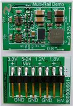
Bottom View
Figure 1. LMR24220 Multi-Rail Reference Board - Top
View
VIN to 3.3V
Vin
5V ± 32V
3.3V
U2
L2
VIN
Ron
EN
Ci2b
Ci3b
Figure 2. LMR24220 Multi-Rail Reference Board Bottom View
L1
BST
RON
LMR24220
FB
EN
Ret
SS
Ci2a
VCC
Co2a
C10
Cc1
RT3
VIN
RB3
Ci1a
GND
FB
EN
VREF
VCON
3.3V
LMZ10501
FB
SGND
3.3V
VREF
VCON
RB
3.3V Rail
Indicator
LED
U3
U1
RT
Co2c
Cvcc
3.3V to 1.2V
EN
Co2b
R2
3.3V to 1.8V
3.3V
R1
Cbt
GND
Css
D2
Reb
GND
SW
Cc3
VIN
LMZ10501
FB
VOUT
1.8V
SGND
Ci3a
RLED
GND
VOUT
FB
3.3V
3.3V
1.2V
D1
Co3a
Co1a
GND
GND
Figure 3. LMR24220 Reference Board Schematic
Table 1. Bill of Materials (BOM) LMR24220
2
Designation
Description
Size
Manufacturer Part #
Vendor
U1
LMZ10501
SE08A
LMZ10501
TI
U2
LMR24220
28-ball DSBGA
LMR24220
TI
U3
LMZ10501
SE08A
LMZ10501
TI
C10
Cap 10nF 25V X7R
0402
C1005X7R1E103K
TDK
Cbt, Ci2a,
Co2a
Cap 0.047µF 50V X7R
0603
GRM188R71H473KA61D
Murata
Cc1, Cc3
Cap 1000pF 25V X7R
0201
GRM033R71E102KA01D
Murata
Ci1a, Ci3a,
Co1a, Co3a
Cap 4.7µF 6.3V X5R
0603
C1608X5R0J475M
TDK
Ci2b, Ci3b
Cap 10µF 35V X5R
1206
GRM31CR6YA106KA12L
Murata
AN-2193 LMR24220 Multi-Rail Reference Board
SNVA505A – September 2011 – Revised April 2013
Submit Documentation Feedback
Copyright © 2011–2013, Texas Instruments Incorporated
�Test Setup
www.ti.com
Table 1. Bill of Materials (BOM) LMR24220 (continued)
5
Designation
Description
Size
Manufacturer Part #
Vendor
Ci2b, Ci3b
(alt)
Cap 10µF 50V X5R
1210
UMK325BJ106MMT
Taiyo Yuden
Co2b, Co2c
Cap 47µF 6.3V X5R
1206
C3216X5R0J476M
TDK
Css
Cap 22nF 16V X7R
0402
C1005X7R1C223K
TDK
Cvcc
Cap 1µF 25V X7R
0805
GCM21BR71E105KA56L
Murata
Panasonic
D1
LED, Blue, SMD
0402
LNJ947W8CRA
D2
Zener Diode 4.3V 200mW
SOD-523F
MM5Z4V3
Fairchild
L1
Shielded Inductor 6.8µH 2.4A
(5.49mm x
5.18mm x
2.00mm)
IHLP2020BZER6R8M01
Vishay-Dale
L2
LTCC Inductor 2.2µH 0.9A
(2.50mm x
1.50mm x
1.20mm)
CPL2512T2R2M
Vishay-Dale
R1
RES, 6.81k ohm, 1%, 0.063W
0402
CRCW04026K81FKED
Vishay-Dale
R2
RES, 2.21k ohm, 1%, 0.063W
0402
CRCW04022K21FKED
Vishay-Dale
Reb
RES, 12.4k ohm, 1%, 0.063W
0402
CRCW040212K4FKED
Vishay-Dale
Ret
RES, 28.0k ohm, 1%, 0.063W
0402
CRCW040228K0FKED
Vishay-Dale
Ron
RES, 76.8k ohm, 1%, 0.063W
0402
CRCW040276K8FKED
Vishay-Dale
Rb, Rb3
RES, 82.5k ohm, 1%, 0.063W
0402
CRCW040282K5FKED
Vishay-Dale
Rt
RES, 187k ohm, 1%, 0.063W
0402
CRCW0402187KFKED
Vishay-Dale
Rt3
RES, 316k ohm, 1%, 0.063W
0402
CRCW0402316KFKED
Vishay-Dale
Rled
RES, 332 ohm, 1%, 0.063W
0402
CRCW0402332RFKED
Vishay-Dale
J1
0.100" (2.54mm), Surface Mount Header, 1x8,
Gold plated,Right Angle
961108-5500-AR-PR
3M
J2
0.100" (2.54 mm) Female Header: 1x8-Pin,
Straight
960108-6202-AR
3M
Test Setup
Table 2. Pin Descriptions
Pin
Name
Description
1
3.3 V
3.3 V Output Voltage — Output from the LMR24220 (U2). Supplies current to both the LMZ10501s and any
external load. Total Current up to 1.5 Amps without airflow. 2 Amps with airflow.
2, 4, 6
GND
Ground — Reference point for all stated voltages.
3
VIN
Input supply — Nominal operating range is 5 V to 32 V. To increase the maximum operating voltage of the
design to 42 V, use the alternate Ci2b, and Ci3b capacitors called out in the BOM.
5
1.2V
1.2 V Output Voltage — Output from the LMZ10501 (U1). Load current up to 1A.
7
1.8V
1.8 V Output Voltage — Output from the LMZ10501 (U3). Load current up to 1A.
8
EN
Enable — Input to the LMR24220 precision enable comparator. Rising threshold is 1.274 V typical. Leave
floating to allow the resistor divider to enable the reference board when VIN exceeds 4 V.
SNVA505A – September 2011 – Revised April 2013
Submit Documentation Feedback
AN-2193 LMR24220 Multi-Rail Reference Board
Copyright © 2011–2013, Texas Instruments Incorporated
3
�Typical Performance Characteristics
www.ti.com
Table 3. Demonstration Board Quick Setup Procedures
Step
6
Description
Notes
1
Connect a power supply to VIN terminal
VIN range: 5 V to 32 V
2
Connect a load to 3.3 V / 1.8 V / 1.2 V terminals
IOUT range: 0A to 1.0A
3
EN should be left floating for normal operation. Short this to ground to
shutdown the part
4
Set VIN = 12 V, with 0A load applied, check 3.3 V / 1.8 V / 1.2 V rails with a
voltmeter
5
Apply a 1.0A load to any rail and check 3.3 V / 1.8 V / 1.2 V rails with a
voltmeter
Typical Performance Characteristics
Efficiency
vs.
Load Current LMR24220, VOUT = 3.3V
Efficiency
vs.
Load Current LMZ10501, VOUT = 1.2V
90
100
90
EFFICIENCY (%)
EFFICIENCY (%)
80
70
60
50
80
70
60
50
40
40
30
0.0
30
VIN = 12V
VIN = 24V
0.5
1.0
1.5
LOAD CURRENT (A)
VIN = 3.3V
20
2.0
0.0 0.1 0.2 0.3 0.4 0.5 0.6 0.7 0.8 0.9 1.0
LOAD CURRENT (A)
Efficiency
vs.
Load Current LMZ10501, VOUT = 1.8V
Startup Waveform
100
EN
EFFICIENCY (%)
90
1V/Div
80
70
60
3.3V
1V/Div
50
1.8V
1V/Div
1.2V
1V/Div
40
30
20
VIN = 3.3V
500 Ps/DIV
0.0 0.1 0.2 0.3 0.4 0.5 0.6 0.7 0.8 0.9 1.0
LOAD CURRENT (A)
4
AN-2193 LMR24220 Multi-Rail Reference Board
SNVA505A – September 2011 – Revised April 2013
Submit Documentation Feedback
Copyright © 2011–2013, Texas Instruments Incorporated
�Layout
www.ti.com
Output Ripple
1.8V
1.2V
Output Power Tradeoff
2.00
30 mV/Div
3.3V RAIL MAXIMUM LOAD (A)
3.3V
30 mV/Div
30 mV/Div
1.75
1.50
1.25
1.00
0.75
0.50
0.25
0.00
5 Ps/DIV
No Airflow. 85C Max Junction
Airflow
0.0
0.5
1.0
1.5
2.0
2.5
3.0
1.2V AND 1.8V RAILS TOTAL OUTPUT POWER (W)
7
Layout
Figure 4. Top Layer
Figure 5. Top Overlay
Figure 6. Mid Layer1 (GND)
SNVA505A – September 2011 – Revised April 2013
Submit Documentation Feedback
AN-2193 LMR24220 Multi-Rail Reference Board
Copyright © 2011–2013, Texas Instruments Incorporated
5
�Layout
www.ti.com
Figure 7. Mid Layer2 (3.3V)
Figure 8. Bottom Layer
Figure 9. Bottom Overlay
6
AN-2193 LMR24220 Multi-Rail Reference Board
SNVA505A – September 2011 – Revised April 2013
Submit Documentation Feedback
Copyright © 2011–2013, Texas Instruments Incorporated
�IMPORTANT NOTICE
Texas Instruments Incorporated and its subsidiaries (TI) reserve the right to make corrections, enhancements, improvements and other
changes to its semiconductor products and services per JESD46, latest issue, and to discontinue any product or service per JESD48, latest
issue. Buyers should obtain the latest relevant information before placing orders and should verify that such information is current and
complete. All semiconductor products (also referred to herein as “components”) are sold subject to TI’s terms and conditions of sale
supplied at the time of order acknowledgment.
TI warrants performance of its components to the specifications applicable at the time of sale, in accordance with the warranty in TI’s terms
and conditions of sale of semiconductor products. Testing and other quality control techniques are used to the extent TI deems necessary
to support this warranty. Except where mandated by applicable law, testing of all parameters of each component is not necessarily
performed.
TI assumes no liability for applications assistance or the design of Buyers’ products. Buyers are responsible for their products and
applications using TI components. To minimize the risks associated with Buyers’ products and applications, Buyers should provide
adequate design and operating safeguards.
TI does not warrant or represent that any license, either express or implied, is granted under any patent right, copyright, mask work right, or
other intellectual property right relating to any combination, machine, or process in which TI components or services are used. Information
published by TI regarding third-party products or services does not constitute a license to use such products or services or a warranty or
endorsement thereof. Use of such information may require a license from a third party under the patents or other intellectual property of the
third party, or a license from TI under the patents or other intellectual property of TI.
Reproduction of significant portions of TI information in TI data books or data sheets is permissible only if reproduction is without alteration
and is accompanied by all associated warranties, conditions, limitations, and notices. TI is not responsible or liable for such altered
documentation. Information of third parties may be subject to additional restrictions.
Resale of TI components or services with statements different from or beyond the parameters stated by TI for that component or service
voids all express and any implied warranties for the associated TI component or service and is an unfair and deceptive business practice.
TI is not responsible or liable for any such statements.
Buyer acknowledges and agrees that it is solely responsible for compliance with all legal, regulatory and safety-related requirements
concerning its products, and any use of TI components in its applications, notwithstanding any applications-related information or support
that may be provided by TI. Buyer represents and agrees that it has all the necessary expertise to create and implement safeguards which
anticipate dangerous consequences of failures, monitor failures and their consequences, lessen the likelihood of failures that might cause
harm and take appropriate remedial actions. Buyer will fully indemnify TI and its representatives against any damages arising out of the use
of any TI components in safety-critical applications.
In some cases, TI components may be promoted specifically to facilitate safety-related applications. With such components, TI’s goal is to
help enable customers to design and create their own end-product solutions that meet applicable functional safety standards and
requirements. Nonetheless, such components are subject to these terms.
No TI components are authorized for use in FDA Class III (or similar life-critical medical equipment) unless authorized officers of the parties
have executed a special agreement specifically governing such use.
Only those TI components which TI has specifically designated as military grade or “enhanced plastic” are designed and intended for use in
military/aerospace applications or environments. Buyer acknowledges and agrees that any military or aerospace use of TI components
which have not been so designated is solely at the Buyer's risk, and that Buyer is solely responsible for compliance with all legal and
regulatory requirements in connection with such use.
TI has specifically designated certain components as meeting ISO/TS16949 requirements, mainly for automotive use. In any case of use of
non-designated products, TI will not be responsible for any failure to meet ISO/TS16949.
Products
Applications
Audio
www.ti.com/audio
Automotive and Transportation
www.ti.com/automotive
Amplifiers
amplifier.ti.com
Communications and Telecom
www.ti.com/communications
Data Converters
dataconverter.ti.com
Computers and Peripherals
www.ti.com/computers
DLP® Products
www.dlp.com
Consumer Electronics
www.ti.com/consumer-apps
DSP
dsp.ti.com
Energy and Lighting
www.ti.com/energy
Clocks and Timers
www.ti.com/clocks
Industrial
www.ti.com/industrial
Interface
interface.ti.com
Medical
www.ti.com/medical
Logic
logic.ti.com
Security
www.ti.com/security
Power Mgmt
power.ti.com
Space, Avionics and Defense
www.ti.com/space-avionics-defense
Microcontrollers
microcontroller.ti.com
Video and Imaging
www.ti.com/video
RFID
www.ti-rfid.com
OMAP Applications Processors
www.ti.com/omap
TI E2E Community
e2e.ti.com
Wireless Connectivity
www.ti.com/wirelessconnectivity
Mailing Address: Texas Instruments, Post Office Box 655303, Dallas, Texas 75265
Copyright © 2013, Texas Instruments Incorporated
�