Product
Folder
Order
Now
Support &
Community
Tools &
Software
Technical
Documents
LMR34206-Q1
SNVSBA8A – MAY 2019 – REVISED OCTOBER 2019
LMR34206-Q1 4.2-V to 42-V, 0.6-A Ultra-Small Synchronous Step-Down Converter
1 Features
2 Applications
•
•
•
•
•
1
•
•
•
•
•
AEC-Q100-qualified for automotive applications:
– Temperature grade 1: –40°C to +125°C, TA
Designed for automotive applications
– Junction temperature range –40°C to +150°C
– Protection features: thermal shutdown, input
undervoltage lockout, cycle-by-cycle current
limit, hiccup short-circuit protection
– 0.2-V dropout with 0.6-A load (typical)
– ±1.5% reference voltage tolerance
– 3.3-V, 5-V fixed-output voltage options
Suited for scalable power supplies
– Pin compatible with:
– LMR36015/06-Q1 (60 V, 0.6 A or 1.5 A)
– LMR33620/30-Q1 (36 V, 2 A, or 3 A)
– 2.1-MHz frequency option
Integration reduces solution size and cost
– Small, 2-mm × 3-mm VQFN package with
wettable flanks
– Few external components
Low power dissipation across load spectrum
– Increased light load efficiency in PFM
– Low operating quiescent current of 24 µA
Optimized for ultra low EMI requirements
– Meets CISPR25 class 5 standard
– Hotrod™ package minimizes switch node
ringing
– Parallel input path minimizes parasitic
inductance
– Spread spectrum reduces peak emissions
ADAS camera module
Head-up display
Body control module
General purpose wide VIN power supplies
3 Description
The LMR34206-Q1 regulator is an easy-to-use,
synchronous, step-down DC/DC converter. With
integrated high-side and low-side power MOSFETs,
up to of output current is delivered over a wide input
voltage range of 4.2 V to 42 V.
The LMR34206-Q1 uses peak-current-mode control
to provide optimal efficiency and output voltage
accuracy. Precision enable gives flexibility by
enabling a direct connection to the wide input voltage
or precise control over device start-up and shutdown.
The power-good flag, with built-in filtering and delay,
offers a true indication of system status eliminating
the requirement for an external supervisor.
The LMR34206-Q1 is in a HotRod™ package which
enables low EMI, higher efficiency, and the smallest
package to die ratio. The device requires few external
components and has a pinout designed for simple
PCB layout. The small solution size and feature set of
the LMR34206-Q1 are designed to simplify
implementation for a wide range of end equipment.
Device Information(1)
PART NUMBER
LMR34206-Q1
PACKAGE
BODY SIZE (NOM)
VQFN-HR (12)
2.00 mm × 3.00 mm
(1) For all available packages, see the orderable addendum at
the end of the data sheet.
Figure 1. Simplified Schematic
BOOT
VIN
VIN
CIN
CBOOT
EN
VOUT
SW
L1
COUT
PGND
LMR34206-Q1
PG
VCC
CVCC
FB
AGND
1
An IMPORTANT NOTICE at the end of this data sheet addresses availability, warranty, changes, use in safety-critical applications,
intellectual property matters and other important disclaimers. PRODUCTION DATA.
�LMR34206-Q1
SNVSBA8A – MAY 2019 – REVISED OCTOBER 2019
www.ti.com
Table of Contents
1
2
3
4
5
6
7
8
Features ..................................................................
Applications ...........................................................
Description .............................................................
Revision History.....................................................
Device Comparison Table.....................................
Pin Configuration and Functions .........................
Specifications.........................................................
1
1
1
2
3
4
5
7.1
7.2
7.3
7.4
7.5
7.6
7.7
7.8
5
5
5
6
6
7
8
9
Absolute Maximum Ratings ......................................
ESD Ratings..............................................................
Recommended Operating Conditions ......................
Thermal Information ..................................................
Electrical Characteristics...........................................
Timing Requirements ................................................
System Characteristics .............................................
Typical Characteristics ..............................................
Detailed Description ............................................ 10
8.1 Overview ................................................................. 10
8.2 Functional Block Diagram ....................................... 11
8.3 Feature Description................................................. 11
8.4 Device Functional Modes........................................ 16
9
Application and Implementation ........................ 20
9.1 Application Information............................................ 20
9.2 Typical Application ................................................. 20
10 Power Supply Recommendations ..................... 29
11 Layout................................................................... 30
11.1 Layout Guidelines ................................................. 30
11.2 Layout Example .................................................... 32
12 Device and Documentation Support ................. 33
12.1
12.2
12.3
12.4
12.5
12.6
12.7
Device Support ....................................................
Documentation Support ........................................
Receiving Notification of Documentation Updates
Support Resources ...............................................
Trademarks ...........................................................
Electrostatic Discharge Caution ............................
Glossary ................................................................
33
33
33
34
34
34
34
13 Mechanical, Packaging, and Orderable
Information ........................................................... 34
4 Revision History
NOTE: Page numbers for previous revisions may differ from page numbers in the current version.
Changes from Original (May 2019) to Revision A
Page
•
Added EMI description to the Features .................................................................................................................................. 1
•
Replaced Figure 36 with the correct graph .......................................................................................................................... 27
2
Submit Documentation Feedback
Copyright © 2019, Texas Instruments Incorporated
Product Folder Links: LMR34206-Q1
�LMR34206-Q1
www.ti.com
SNVSBA8A – MAY 2019 – REVISED OCTOBER 2019
5 Device Comparison Table
ORDERABLE PART
NUMBER
OUTPUT VOLTAGE
SPREAD
SPECTRUM
FPWM
fSW
PACKAGE QUANTITY
LMR34206FSC3RNXTQ1
3.3-V fixed
Yes
Yes
2.1 MHz
250
3000
LMR34206FSC3RNXRQ1
3.3-V fixed
Yes
Yes
2.1 MHz
LMR34206SC3QRNXTQ1
3.3-V fixed
Yes
No
2.1 MHz
250
LMR34206SC3QRNXRQ1
3.3-V fixed
Yes
No
2.1 MHz
3000
LMR34206FSC5RNXTQ1
5-V fixed
Yes
Yes
2.1 MHz
250
3000
LMR34206FSC5RNXRQ1
5-V fixed
Yes
Yes
2.1 MHz
LMR34206SC5QRNXTQ1
5-V fixed
Yes
No
2.1 MHz
250
LMR34206SC5QRNXRQ1
5-V fixed
Yes
No
2.1 MHz
3000
Submit Documentation Feedback
Copyright © 2019, Texas Instruments Incorporated
Product Folder Links: LMR34206-Q1
3
�LMR34206-Q1
SNVSBA8A – MAY 2019 – REVISED OCTOBER 2019
www.ti.com
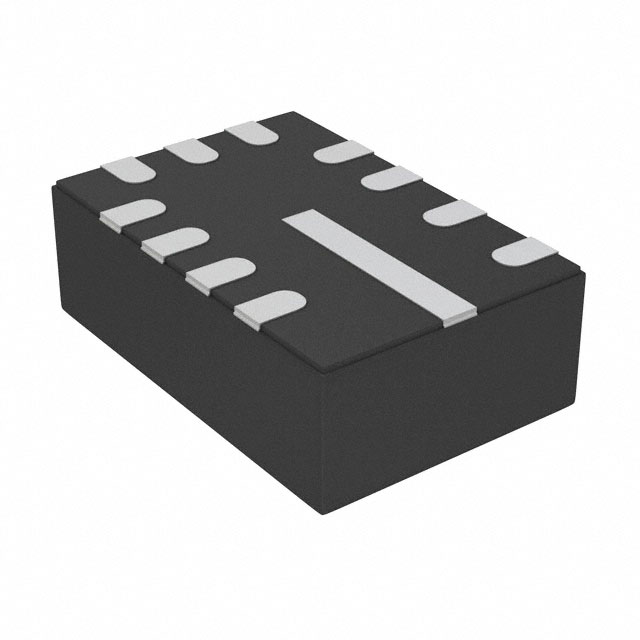
6 Pin Configuration and Functions
RNX Package
12-Pin VQFN-HR
Top View
SW
12
5
PGND 1
11 PGND
10 VIN
VIN 2
NC
3
9 EN
BOOT
4
8 PG
5
6
7
VCC AGND FB
Pin Functions
NO.
NAME
TYPE
DESCRIPTION
1, 11
PGND
G
Power ground terminal. Connect to system ground and AGND. Connect to CIN with short wide traces.
2, 10
VIN
P
Input supply to regulator. Connect to CIN with short wide traces.
3
NC
—
Connect the SW pin to NC on the PCB. This simplifies the connection from the CBOOT capacitor to the
SW pin. This pin has no internal connection to the regulator.
4
BOOT
P
Boot-strap supply voltage for internal high-side driver. Connect a high-quality 100-nF capacitor from this
pin to the SW pin. Connect the SW pin to NC on the PCB. This simplifies the connection from the CBOOT
capacitor to the SW pin.
5
VCC
P
Internal 5-V LDO output. Used as supply to internal control circuits. Do not connect to external loads.
Can be used as logic supply for power-good flag. Connect a high-quality 1-µF capacitor from this pin to
GND.
6
AGND
G
Analog ground for regulator and system. Ground reference for internal references and logic. All electrical
parameters are measured with respect to this pin. Connect to system ground on PCB.
7
FB
A
Feedback input to regulator. Connect to tap point of feedback voltage divider. DO NOT FLOAT. DO
NOT GROUND.
8
PG
A
Open drain power-good flag output. Connect to suitable voltage supply through a current limiting
resistor. High = power OK, low = power bad. Goes low when EN = Low. Can be open or grounded when
not used.
9
EN
A
Enable input to regulator. High = ON, low = OFF. Can be connected directly to VIN; DO NOT FLOAT.
12
SW
P
Regulator switch node. Connect to power inductor. Connect the SW pin to NC on the PCB. This
simplifies the connection from the CBOOT capacitor to the SW pin.
A = Analog, P = Power, G = Ground
4
Submit Documentation Feedback
Copyright © 2019, Texas Instruments Incorporated
Product Folder Links: LMR34206-Q1
�LMR34206-Q1
www.ti.com
SNVSBA8A – MAY 2019 – REVISED OCTOBER 2019
7 Specifications
7.1 Absolute Maximum Ratings
Over operating junction temperature range of -40°C to 150°C (unless otherwise noted) (1)
MIN
MAX
VIN to PGND
–0.3
45
V
EN to AGND
–0.3
45.3
V
FB to AGND
–0.3
5.5
V
PG to AGND
–0.3
22
V
AGND to PGND
–0.3
0.3
V
SW to PGND
–0.3
45.3
V
SW to PGND less than 10-ns negative transient
–3.5
CBOOT to SW
–0.3
5.5
VCC to AGND
–0.3
5.5
V
Junction Temperature TJ
-40
150
°C
Storage temperature, Tstg
–65
150
°C
Input voltage
Output voltage
(1)
UNIT
V
V
Stresses beyond those listed under Absolute Maximum Ratings may cause permanent damage to the device. These are stress ratings
only, which do not imply functional operation of the device at these or any other conditions beyond those indicated under Recommended
Operating Conditions. Exposure to absolute-maximum-rated conditions for extended periods may affect device reliability.
7.2 ESD Ratings
V(ESD)
Electrostatic
discharge
Human-body model (HBM), per AEC Q100-002 (1)
HBM ESD Classification Level 2
V(ESD)
Electrostatic
discharge
Charged-device model (CDM), per AEC Q100-011
CDM ESD Classification Level C5
(1)
VALUE
UNIT
±2500
V
±750
V
AEC Q100-002 indicates that HBM stressing shall be in accordance with ANSI/ESDA/JEDEC JS-001 specification
7.3 Recommended Operating Conditions
Over the recommended operating junction temperature range of –40 ℃ to 150 ℃ (unless otherwise noted) (1)
MIN
MAX
4.2
42
V
EN to PGND (2)
0
42
V
(2)
0
18
V
0
0.6
A
VIN to PGND
Input voltage
PG to PGND
Output current
(1)
(2)
IOUT
UNIT
Recommended operating conditions indicate conditions for which the device is intended to be functional, but do not ensure specific
performance limits. For ensured specifications, see Electrical Characteristics.
The voltage on this pin must not exceed the voltage on the VIN pin by more than 0.3 V.
Submit Documentation Feedback
Copyright © 2019, Texas Instruments Incorporated
Product Folder Links: LMR34206-Q1
5
�LMR34206-Q1
SNVSBA8A – MAY 2019 – REVISED OCTOBER 2019
www.ti.com
7.4 Thermal Information
The value of RθJA given in this table is only valid for comparison with other packages and can not be used for design
purposes. These values were calculated in accordance with JESD 51-7 and simulated on a 4-Layer JEDEC board. They do
not represent the performance obtained in an actual application. For design information see Maximum Ambient
Temperature section.
LMR34206-Q1
THERMAL METRIC (1) (2)
RNX (VQFN-HR)
UNIT
12 PINS
RθJA
Junction-to-ambient thermal resistance
72.5
°C/W
RθJC(top)
Junction-to-case (top) thermal resistance
35.9
°C/W
RθJB
Junction-to-board thermal resistance
23.3
°C/W
ψJT
Junction-to-top characterization parameter
0.8
°C/W
ψJB
Junction-to-board characterization parameter
23.5
°C/W
(1)
(2)
For more information about traditional and new thermal metrics, see the Semiconductor and IC Package Thermal Metrics application
report.
The value of RθJA given in this table is only valid for comparison with other packages and can not be used for design purposes. These
values were calculated in accordance with JESD 51-7 and simulated on a 4-Layer JEDEC board. They do not represent the
performance obtained in an actual application. For design information see Maximum Ambient Temperature section.
7.5 Electrical Characteristics
Limits apply over operating junction temperature (TJ ) range of –40°C to +150°C, unless otherwise stated. Minimum and
Maximum limits (1) are specified through test, design or statistical correlation. Typical values represent the most likely
parametric norm at TJ = 25°C, and are provided for reference purposes only. Unless otherwise stated, the following conditions
apply: VIN = 12V.
PARAMETER
TEST CONDITIONS
MIN
TYP
MAX
14
24
35
UNIT
SUPPLY VOLTAGE (VIN PIN)
IQ-nonSW
Operating quiescent current (nonswitching) (2)
VEN = 3.3 V (PFM variant only)
ISD
Shutdown quiescent current;
measured at VIN pin
VEN = 0 V
3.3
µA
µA
ENABLE (EN PIN)
VEN-VCC-H
Enable input high level for VCC output
VENABLE rising; Internal LDO turns ON
VEN-VCC-L
Enable input low level for VCC output
VENABLE falling; Internal LDO turns
OFF
1.14
VEN-VOUT-H
Enable input high level for VOUT
VENABLE rising; Switching ON
1.157
1.231
1.3
V
VEN-VOUT-HYS
Enable input hysteresis for VOUT
Hysteresis below VEN-VOUT-H;
Switching OFF
45
110
175
mV
ILKG-EN
Enable input leakage current
VEN = 3.3V
0.2
50
nA
4.75
5
5.25
V
0.3
V
V
INTERNAL LDO (VCC PIN)
VCC
VCC-UVLORising
VCC-UVLOFalling
Internal VCC voltage
6 V ≤ VIN ≤ 42 V
Internal VCC undervoltage lockout
VCC rising
3.6
3.8
4.0
V
Internal VCC undervoltage lockout
VCC falling
3.1
3.3
3.5
V
VOLTAGE REFERENCE (FB PIN)
V5v0-Fixed
5 V Fixed Output voltage
Fixed output voltage option
4.9
5
5.1
V
V3v3-Fixed
3.3 V Fixed Output voltage
Fixed output voltage option
3.23
3.3
3.37
V
ILKG-5v0-Fixed
Feedback leakage current; 5v0 Fixed
VOUT = 5 V (Fixed output voltage
option only)
2.5
2.9
µA
ILKG-3v3V-Fixed
Feedback leakage current; 3v3 Fixed
VOUT = 3.3 V (Fixed output voltage
option only)
1.4
1.8
µA
(1)
(2)
6
MIN and MAX limits are 100% production tested at 25℃. Limits over the operating temperature range verified through correlation using
Statistical Quality Control (SQC) methods. Limits are used to calculate Average Outgoing Quality Level (AOQL).
This is the current used by the device open loop. It does not represent the total input current of the system when in regulation.
Submit Documentation Feedback
Copyright © 2019, Texas Instruments Incorporated
Product Folder Links: LMR34206-Q1
�LMR34206-Q1
www.ti.com
SNVSBA8A – MAY 2019 – REVISED OCTOBER 2019
Electrical Characteristics (continued)
Limits apply over operating junction temperature (TJ ) range of –40°C to +150°C, unless otherwise stated. Minimum and
Maximum limits(1) are specified through test, design or statistical correlation. Typical values represent the most likely
parametric norm at TJ = 25°C, and are provided for reference purposes only. Unless otherwise stated, the following conditions
apply: VIN = 12V.
PARAMETER
TEST CONDITIONS
MIN
TYP
MAX
UNIT
CURRENT LIMITS AND HICCUP
ISC
High-side current limit (3)
0.8
1
1.2
A
ILS-LIMIT
Low-side current limit (3)
0.6
0.8
0.95
A
IL-ZC
Zero cross detector threshold
IPEAK-MIN
Minimum inductor peak current (3)
IL-NEG
Negative current limit (3)
PFM variants only
0.02
A
0.18
A
FPWM variant only
-0.95
–0.6
–0.25
A
POWER GOOD (PGOOD PIN)
VPG-HIGH-UP
Power-Good upper threshold - rising
% of FB voltage
105%
107%
110%
VPG-LOW-DN
Power-Good lower threshold - falling
% of FB voltage
90%
93%
95%
VPG-HYS
Power-Good hysteresis (rising &
falling)
% of FB voltage
TPG
Power-Good rising/falling edge
deglitch delay
VPG-VALID
Minimum input voltage for proper
Power-Good function
RPG
Power-Good on-resistance
VEN = 2.5 V
RPG
Power-Good on-resistance
VEN = 0 V
Internal oscillator frequency
2.1-MHz variant
RDS-ON-HS
High-side MOSFET ON-resistance
RDS-ON-LS
Low-side MOSFET ON-resistance
2%
80
140
200
µs
2
V
80
165
Ω
35
90
Ω
2.1
2.35
MHz
IOUT = 0.5 A
225
435
mΩ
IOUT = 0.5 A
150
280
mΩ
OSCILLATOR
FOSC
1.95
MOSFETS
(3)
The current limit values in this table are tested, open loop, in production. They may differ from those found in a closed loop application.
7.6 Timing Requirements
Limits apply over operating junction temperature (TJ ) range of –40°C to +150°C, unless otherwise stated. Minimum and
Maximum limits (1) are specified through test, design or statistical correlation. Typical values represent the most likely
parametric norm at TJ = 25°C, and are provided for reference purposes only. Unless otherwise stated, the following conditions
apply: VIN = 12 V.
NOM
MAX
tON-MIN
Minimum switch on-time
MIN
55
83
tOFF-MIN
Minimum switch off-time
53
73
ns
tON-MAX
Maximum switch on-time
7
12
µs
tSS
Internal soft-start time
4.5
6
ms
(1)
3
UNIT
ns
MIN and MAX limits are 100% production tested at 25℃. Limits over the operating temperature range verified through correlation using
Statistical Quality Control (SQC) methods. Limits are used to calculate Average Outgoing Quality Level (AOQL).
Submit Documentation Feedback
Copyright © 2019, Texas Instruments Incorporated
Product Folder Links: LMR34206-Q1
7
�LMR34206-Q1
SNVSBA8A – MAY 2019 – REVISED OCTOBER 2019
www.ti.com
7.7 System Characteristics
The following specifications apply to a typical application circuit with nominal component values. Specifications in the typical
(TYP) column apply to TJ = 25℃ only. Specifications in the minimum (MIN) and maximum (MAX) columns apply to the case
of typical components over the temperature range of TJ = –40℃ to 150℃. These specifications are not ensured by production
testing.
PARAMETER
TEST CONDITIONS
MIN
TYP
UNIT
Operating input voltage range
VOUT
Voltage regulation for VOUT = 3.3 V
fixed (1)
FPWM operation
ISUPPLY
Input supply current when in regulation
VIN = 12 V, VOUT = 3.3 V Fixed, PFM variant
DMAX
Maximum switch duty cycle (2)
VHC
FB pin voltage required to trip short-circuit
hiccup mode
0.4
V
tHC
Time between current-limit hiccup burst
94
ms
tD
Switch voltage dead time
2
ns
FsSS
Frequency span of spread spectrum
operation
±4
%
FrSS
Triangular spread spectrum repetition
frequency
16
kHz
TSD
Thermal shutdown temperature
Shutdown temperature
170
°C
TSD
Thermal shutdown temperature
Recovery temperature
158
°C
(1)
(2)
8
4.2
MAX
VIN
3.28
3.33
26
42
V
3.37
V
µA
98%
Deviation in VOUT from nominal output voltage value at VIN = 24 V, IOUT = 0 A to 0.6A
In dropout the switching frequency drops to increase the effective duty cycle. The lowest frequency is clamped at approximately: FMIN =
1 / (tON-MAX + tOFF-MIN). DMAX = tON-MAX /(tON-MAX + tOFF-MIN).
Submit Documentation Feedback
Copyright © 2019, Texas Instruments Incorporated
Product Folder Links: LMR34206-Q1
�LMR34206-Q1
www.ti.com
SNVSBA8A – MAY 2019 – REVISED OCTOBER 2019
7.8 Typical Characteristics
Unless otherwise specified the following conditions apply: TA = 25°C. VIN = 24 V.
30
12
29
10
Shutdown Current (µA)
Quiescent Current (µA)
28
27
26
25
24
23
22
8
6
4
25C
150C
-40C
21
20
2
6
10
14
18
22
26
30
Input Voltage (V)
34
38
42
6
10
VFB = 1 V
22
26
30
Input Voltage (V)
34
38
42
Shut
Figure 3. Shutdown Supply Current
1.5
1
1.3
0.8
Current (A)
Current (A)
18
EN = 0 V
Figure 2. Non-Switching Input Supply Current
1.1
0.9
0.6
0.4
0.2
0.7
0.5
-40
0
40
80
Temperatuer (°C)
120
0
-40
150
hs-c
0
120
150
ls-c
Figure 5. Low Side Current Limit
Figure 4. High Side Current Limit
425
1.016
400
Peak Inductor Current (mA)
1.02
1.012
1.008
1.004
1
0.996
0.992
0.988
375
350
325
300
275
250
225
0.984
0.98
-40
40
80
Temperature (°C)
VIN = 24 V
VIN = 24 V
Voltage (V)
14
LMR3
200
0
40
80
Temperature (°C)
120
150
vref
5
10
IOUT = 0 A
ƒSW = 2100 kHz
Figure 6. Reference Voltage Drift
15
20
25
30
Input Voltage (V)
35
40
Product Folder Links: LMR34206-Q1
lmr3
VOUT = 3.3V
Figure 7. IPEAK-MIN
Submit Documentation Feedback
Copyright © 2019, Texas Instruments Incorporated
45
9
�LMR34206-Q1
SNVSBA8A – MAY 2019 – REVISED OCTOBER 2019
www.ti.com
8 Detailed Description
8.1 Overview
The LMR34206-Q1 is a synchronous peak-current-mode buck regulator designed for a wide variety of
applications. The regulator automatically switches modes between PFM and PWM depending on load. At heavy
loads, the device operates in PWM at a constant switching frequency. At light loads the mode changes to PFM,
with diode emulation allowing DCM. This reduces the input supply current and keeps efficiency high. The device
features internal loop compensation which reduces design time and requires fewer external components than
externally compensated regulators.
The LMR34206-Q1 is designed with a flip-chip or HotRod™ technology, greatly reducing the parasitic inductance
of pins. In addition, the layout of the device allows for reduction in the radiated noise generated by the switching
action through partial cancellation of the current generated magnetic field. As a result the switch-node waveform
exhibits less overshoot and ringing.
2V/div
50ns/div
BW:500MHz
Figure 8. Switch Node Waveform
10
Submit Documentation Feedback
Copyright © 2019, Texas Instruments Incorporated
Product Folder Links: LMR34206-Q1
�LMR34206-Q1
www.ti.com
SNVSBA8A – MAY 2019 – REVISED OCTOBER 2019
8.2 Functional Block Diagram
VCC
INT. REG.
BIAS
OSCILLATOR
EN
VIN
ENABLE
LOGIC
BOOT
HS CURRENT
SENSE
1.0V
Reference
ERROR
AMPLIFIER
FB
+
-
PG
+
-
PWM
COMP.
CONTROL
LOGIC
PFM MODE
CONTROL
SW
DRIVER
LS CURRENT
SENSE
POWER GOOD
CONTROL
AGND
PGND
8.3 Feature Description
8.3.1 Power-Good Flag Output
The power-good flag function (PG output pin) of the LMR34206-Q1 can be used to reset a system
microprocessor whenever the output voltage is out of regulation. This open-drain output goes low under fault
conditions, such as current limit and thermal shutdown, as well as during normal start-up. A glitch filter prevents
false flag operation for short excursions of the output voltage, such as during line and load transients. Output
voltage excursions lasting less than tPG do not trip the power-good flag. Power-good operation can best be
understood by reference to Figure 9 and Figure 10. Note that during initial power-up a delay of about 4 ms
(typical) is inserted from the time that EN is asserted to the time that the power-good flag goes high. This delay
only occurs during start-up and is not encountered during normal operation of the power-good function.
The power-good output consists of an open drain NMOS; requiring an external pullup resistor to a suitable logic
supply. It can also be pulled up to either VCC or VOUT, through an appropriate resistor, as desired. If this function
is not needed, the PG pin must be grounded. When EN is pulled low, the flag output is also forced low. With EN
low, power good remains valid as long as the input voltage is ≥ 2 V (typical). Limit the current into this pin to ≤ 4
mA.
Submit Documentation Feedback
Copyright © 2019, Texas Instruments Incorporated
Product Folder Links: LMR34206-Q1
11
�LMR34206-Q1
SNVSBA8A – MAY 2019 – REVISED OCTOBER 2019
www.ti.com
Feature Description (continued)
VOUT
VPG-HIGH_UP (107%)
VPG-HIGH-DN (105%)
VPG-LOW-UP (95%)
VPG-LOW-DN (93%)
PG
High = Power Good
Low = Fault
Figure 9. Static Power-Good Operation
12
Submit Documentation Feedback
Copyright © 2019, Texas Instruments Incorporated
Product Folder Links: LMR34206-Q1
�LMR34206-Q1
www.ti.com
SNVSBA8A – MAY 2019 – REVISED OCTOBER 2019
Feature Description (continued)
Glitches do not cause false operation nor reset timer
VOUT
VPG-LOW-UP (95%)
VPG-LOW-DN (93%)


 工商网监
湘ICP备2023018690号
工商网监
湘ICP备2023018690号
