User's Guide
SNVU193A – October 2012 – Revised April 2013
AN-2281 LMR61428 Evaluation Module
1
Introduction
The LMR61428 evaluation module is designed to provide the power supply design engineer with a fully
functional regulator design. The evaluation module takes the input from a single Li-Ion battery and boosts
the voltage up to 5V at a constant load capability of 500mA. The switching frequency of the boost
regulator is set to about 1200 kHz which helps in reducing the solution size and keeping switching noise
out of the AM radio band. The printed circuit board consists of 4 layers of copper on FR4 material. The
first middle layer is a solid ground layer which helps in minimizing the AC current loop. This user's guide
contains the evaluation module schematic, a quick setup procedure using a bench power supply, and a
Bill-of-Materials (BOM). For complete circuit design information, see LMR61428 SIMPLE SWITCHER
14Vout, 2.85A Step-Up Voltage Regulator in VSSOP (SNVS815).
2
Features
•
•
•
•
3
One cell Li-Ion battery for Input Voltage
5V Output Voltage at 500mA Output Current
Switching Frequency of 1.2 MHz
Small Solution Size: 2.287 × 1.058 inches (58.09 × 26.87 mm)
Evaluation Board Schematic
L1
1 Cell Li-ion
VIN
SW
5V at 0.5A
VOUT
D1
30203001
U1
J1
+
VOUT
3
2
1
7
BOOT
Rfbt
SW
Cff
8
LMR61428
Rdd
Ren
EN
2
6
Cboot
Rt
3
Cdd
+
4
EN
Cin
VDD
FB
PGND
FREQ SGND
Co1
Co2
1 GND
5
Rfbb
GND
Figure 1. LMR61428 Evaluation Module Schematic
All trademarks are the property of their respective owners.
SNVU193A – October 2012 – Revised April 2013
Submit Documentation Feedback
AN-2281 LMR61428 Evaluation Module
Copyright © 2012–2013, Texas Instruments Incorporated
1
�Powering and Loading Considerations
4
www.ti.com
Powering and Loading Considerations
Read this entire section prior to attempting to power the evaluation board.
4.1
Quick Start Procedure
Step 1: Set the bench power supply current limit to 3A. Set the power supply voltage to 3.5V. Turn off the
power supply output. Connect the power supply to the LMR61428 demo board. Positive connection to VIN
and negative connection to GND.
Step 2: Connect a load, as high as 0.5A, to the VOUT terminal. Positive connection to VOUT and negative
connection to GND.
Step 3: Connect the shunt so as to short the pins 1 and 2 of the jumper J1. This sets the bootstrap to VOUT
Step 4: The EN pin should be left open for normal operation.
Step 5: Turn on the bench power supply with no load applied to the LMR61428. If the shunt for the jumper
J1 was in place, the VOUT would be in regulation at a nominal 5V.
Step 6: Gradually increase the load and VOUT should remain in regulation as the load is increased up to
0.5 Amps.
4.2
Shutdown Operation
The EVM includes a pull-up resistor Ren to enable the device. Use the EN post to disable the device by
pulling this node to GND.
4.3
Bootstrap Operation
The EVM has a jumper installed to select the bootstrap option. The default condition is that the jumper be
set such that the bootstrap voltage is obtained from the output. For more information, see LMR61428
SIMPLE SWITCHER 14Vout, 2.85A Step-Up Voltage Regulator in VSSOP (SNVS815).
4.4
Setting the Output Voltage
The output voltage of the step-up regulator can be set between 1.24V and 14V. But because of the gated
oscillator scheme, the maximum possible input to output boost ratio is fixed. For a boost regulator,
VOUT / VIN = 1 / [1 − D]
(1)
The LMR61428 has a fixed duty cycle, D, of 70% typical. Therefore,
VOUT / VIN = 1 / 0.3
(2)
This sets the maximum possible boost ratio of VIN to VOUT to about 3 times. The user can now estimate
what the minimum design inputs should be in order to achieve a desired output, or what the output would
be when a certain minimum input is applied. For example, if the desired VOUT was 14V, then the least VIN
should be higher than VOUT / 3. If the input voltage fell below this threshold, the output voltage would not
be regulated because of the fixed duty cycle. If the minimum VIN was guaranteed at 2V, the max possible
VOUT would be VIN × 3.
The VOUT is set by connecting a feedback resistive divider made of Rfbt and Rfbb. The feedback resistor
values are selected as follows:
Rfbb = Rfbt /[(VOUT/ 1.24) −1]
(3)
A value of 150kΩ is suggested for Rfbt. Then, Rfbb can be selected using Equation 3. A 39pF capacitor (Cff)
connected across Rfbt helps in feeding back most of the AC ripple at VOUT to the FB pin. This helps reduce
the peak-to-peak output voltage ripple as well as improve the efficiency of the step-up regulator, because
a set hysteresis of 30mV at the FB pin is used for the gated oscillator control scheme.
2
AN-2281 LMR61428 Evaluation Module
SNVU193A – October 2012 – Revised April 2013
Submit Documentation Feedback
Copyright © 2012–2013, Texas Instruments Incorporated
�Powering and Loading Considerations
www.ti.com
Typical Test Setup
Ammeter
A
Ammeter
A
+
VOUT GND
GND
Voltmeter V
Power
Supply
+
-
Electronic
Load
-
4.5
VIN
V
Voltmeter
Demo Board
Figure 2. Efficiency Measurements
Oscilloscope
VOUT
GND
Chf
Figure 3. Voltage Ripple Measurements
SNVU193A – October 2012 – Revised April 2013
Submit Documentation Feedback
AN-2281 LMR61428 Evaluation Module
Copyright © 2012–2013, Texas Instruments Incorporated
3
�Powering and Loading Considerations
www.ti.com
I
I
I
I
I
GND
VOUT
5
6
A
B
C
D
E
F
GND
4
VOUT SENSE+
3
VOUT SENSE -
2
SPARE
1
VIN SENSE+
EN
VIN
I
I
I
I
I
I
I
Figure 4. Edge Connector Schematic
4
AN-2281 LMR61428 Evaluation Module
SNVU193A – October 2012 – Revised April 2013
Submit Documentation Feedback
Copyright © 2012–2013, Texas Instruments Incorporated
�Powering and Loading Considerations
www.ti.com
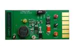
4.6
Board Images
Figure 5. Top Side
SNVU193A – October 2012 – Revised April 2013
Submit Documentation Feedback
AN-2281 LMR61428 Evaluation Module
Copyright © 2012–2013, Texas Instruments Incorporated
5
�Powering and Loading Considerations
www.ti.com
Figure 6. Bottom Side
6
AN-2281 LMR61428 Evaluation Module
SNVU193A – October 2012 – Revised April 2013
Submit Documentation Feedback
Copyright © 2012–2013, Texas Instruments Incorporated
�Typical Performance Characteristics
www.ti.com
5
Typical Performance Characteristics
Efficiency vs. Load Current
VOUT = 5V
Load Transient Waveforms
VIN = 3.6V, IOUT = 50 to 500mA
84
IOUT
82
EFFICIENCY (%)
80
100 mA/Div
78
76
VOUT = 5V
74
Vin = 3.0V
Vin = 3.1V
Vin = 3.2V
Vin = 3.4V
Vin = 3.5V
Vin = 3.6V
Vin = 3.8V
Vin = 4.0V
72
70
68
66
64
50 mV/Div
100 Ps/DIV
0.000.060.120.180.240.300.360.420.480.54
IOUT(A)
Switching Node and Output Voltage Waveforms
VIN = 3.6V, IOUT = 500mA
Startup Waveform
VSW
VOUT = 5V
5V/Div
2V/Div
IOUT = 0.5A 0.5A/Div
VOUT = 5V
VIN = 3V
1V/Div
50 mV/Div
10 Ps/DIV
500 Ps/DIV
SNVU193A – October 2012 – Revised April 2013
Submit Documentation Feedback
AN-2281 LMR61428 Evaluation Module
Copyright © 2012–2013, Texas Instruments Incorporated
7
�Bill of Materials
6
8
www.ti.com
Bill of Materials
ID
Part Number
Type
Size
U1
LMR61428
Boost Regulator
SOT-23
L1
SRU1048-8R2Y
Inductor
SMD
Parameters
Qty
Vendor
1
Texas
Instruments
8.2uH, 4.6A,
0.015 ohm,
1
Bourns
D1
B220A-13-F
Diode
SMA
Schottky, 20V, 2A
1
Toshiba
Cin
293D226X9010C2TE3
Capacitor
SMD
Tantalum, 22uF,
10V
1
VishaySprague
Co1
594D686X0010C2T
Capacitor
SMD
Tantalum, 68uF,
10V
1
VishaySprague
Co2
08053D105KAT2A
Capacitor
0805
Ceramic, 1uF,
25V, X5R
1
AVX
Cdd
C0603C105K4PACTU
Capacitor
0603
Ceramic, 1uF,
16V, X5R
1
Kemet
Cff
GRM1885C2A390JA01D
Capacitor
0603
Ceramic, 39pF,
100V, C0G/NP0
1
MuRata
Rfbt
RG1608P-154-B-T5
Resistor
0603
150 kΩ
1
Susumu Co Ltd
Rfbb
RG1608P-4992-B-T5
Resistor
0603
49.9 kΩ
1
Susumu Co Ltd
Rt
CRCW0603118KFKEA
Resistor
0603
118 kΩ
1
Vishay-Dale
Rdd
CRCW060349R9FKEA
Resistor
0603
49.9 Ω
1
Vishay-Dale
Ren
CRCW060310K0FKEA
Resistor
0603
10.0 kΩ
1
Vishay-Dale
EN
5014
Test Point Loop
Yellow
1
Keystone
VIN
5010
Test Point Loop
Red
1
Keystone
VOUT
5013
Test Point Loop
Orange
1
Keystone
GND
5011
Test Point Loop
Black
2
Keystone
SW
5012
Test Point Loop
White
1
Keystone
J1
PBC03SAAN
Header
100mil, 1x3
1
Sullins
Connector
Solutions
SH-J1
969102-0000-DA
Shunt
100mil, Black
1
3M
AN-2281 LMR61428 Evaluation Module
SNVU193A – October 2012 – Revised April 2013
Submit Documentation Feedback
Copyright © 2012–2013, Texas Instruments Incorporated
�PCB Layout
www.ti.com
7
PCB Layout
Figure 7. Top Copper
Figure 8. Top Overlay
SNVU193A – October 2012 – Revised April 2013
Submit Documentation Feedback
AN-2281 LMR61428 Evaluation Module
Copyright © 2012–2013, Texas Instruments Incorporated
9
�PCB Layout
www.ti.com
Figure 9. Internal Layer 1
Figure 10. Internal Layer 2
10
AN-2281 LMR61428 Evaluation Module
SNVU193A – October 2012 – Revised April 2013
Submit Documentation Feedback
Copyright © 2012–2013, Texas Instruments Incorporated
�PCB Layout
www.ti.com
Figure 11. Bottom Copper
Figure 12. Bottom Overlay
SNVU193A – October 2012 – Revised April 2013
Submit Documentation Feedback
AN-2281 LMR61428 Evaluation Module
Copyright © 2012–2013, Texas Instruments Incorporated
11
�IMPORTANT NOTICE
Texas Instruments Incorporated and its subsidiaries (TI) reserve the right to make corrections, enhancements, improvements and other
changes to its semiconductor products and services per JESD46, latest issue, and to discontinue any product or service per JESD48, latest
issue. Buyers should obtain the latest relevant information before placing orders and should verify that such information is current and
complete. All semiconductor products (also referred to herein as “components”) are sold subject to TI’s terms and conditions of sale
supplied at the time of order acknowledgment.
TI warrants performance of its components to the specifications applicable at the time of sale, in accordance with the warranty in TI’s terms
and conditions of sale of semiconductor products. Testing and other quality control techniques are used to the extent TI deems necessary
to support this warranty. Except where mandated by applicable law, testing of all parameters of each component is not necessarily
performed.
TI assumes no liability for applications assistance or the design of Buyers’ products. Buyers are responsible for their products and
applications using TI components. To minimize the risks associated with Buyers’ products and applications, Buyers should provide
adequate design and operating safeguards.
TI does not warrant or represent that any license, either express or implied, is granted under any patent right, copyright, mask work right, or
other intellectual property right relating to any combination, machine, or process in which TI components or services are used. Information
published by TI regarding third-party products or services does not constitute a license to use such products or services or a warranty or
endorsement thereof. Use of such information may require a license from a third party under the patents or other intellectual property of the
third party, or a license from TI under the patents or other intellectual property of TI.
Reproduction of significant portions of TI information in TI data books or data sheets is permissible only if reproduction is without alteration
and is accompanied by all associated warranties, conditions, limitations, and notices. TI is not responsible or liable for such altered
documentation. Information of third parties may be subject to additional restrictions.
Resale of TI components or services with statements different from or beyond the parameters stated by TI for that component or service
voids all express and any implied warranties for the associated TI component or service and is an unfair and deceptive business practice.
TI is not responsible or liable for any such statements.
Buyer acknowledges and agrees that it is solely responsible for compliance with all legal, regulatory and safety-related requirements
concerning its products, and any use of TI components in its applications, notwithstanding any applications-related information or support
that may be provided by TI. Buyer represents and agrees that it has all the necessary expertise to create and implement safeguards which
anticipate dangerous consequences of failures, monitor failures and their consequences, lessen the likelihood of failures that might cause
harm and take appropriate remedial actions. Buyer will fully indemnify TI and its representatives against any damages arising out of the use
of any TI components in safety-critical applications.
In some cases, TI components may be promoted specifically to facilitate safety-related applications. With such components, TI’s goal is to
help enable customers to design and create their own end-product solutions that meet applicable functional safety standards and
requirements. Nonetheless, such components are subject to these terms.
No TI components are authorized for use in FDA Class III (or similar life-critical medical equipment) unless authorized officers of the parties
have executed a special agreement specifically governing such use.
Only those TI components which TI has specifically designated as military grade or “enhanced plastic” are designed and intended for use in
military/aerospace applications or environments. Buyer acknowledges and agrees that any military or aerospace use of TI components
which have not been so designated is solely at the Buyer's risk, and that Buyer is solely responsible for compliance with all legal and
regulatory requirements in connection with such use.
TI has specifically designated certain components as meeting ISO/TS16949 requirements, mainly for automotive use. In any case of use of
non-designated products, TI will not be responsible for any failure to meet ISO/TS16949.
Products
Applications
Audio
www.ti.com/audio
Automotive and Transportation
www.ti.com/automotive
Amplifiers
amplifier.ti.com
Communications and Telecom
www.ti.com/communications
Data Converters
dataconverter.ti.com
Computers and Peripherals
www.ti.com/computers
DLP® Products
www.dlp.com
Consumer Electronics
www.ti.com/consumer-apps
DSP
dsp.ti.com
Energy and Lighting
www.ti.com/energy
Clocks and Timers
www.ti.com/clocks
Industrial
www.ti.com/industrial
Interface
interface.ti.com
Medical
www.ti.com/medical
Logic
logic.ti.com
Security
www.ti.com/security
Power Mgmt
power.ti.com
Space, Avionics and Defense
www.ti.com/space-avionics-defense
Microcontrollers
microcontroller.ti.com
Video and Imaging
www.ti.com/video
RFID
www.ti-rfid.com
OMAP Applications Processors
www.ti.com/omap
TI E2E Community
e2e.ti.com
Wireless Connectivity
www.ti.com/wirelessconnectivity
Mailing Address: Texas Instruments, Post Office Box 655303, Dallas, Texas 75265
Copyright © 2013, Texas Instruments Incorporated
�