LMR62421XSDDEMO/NOPB 数据手册
User's Guide
SNVA507A – November 2011 – Revised April 2013
AN-2197 LMR62421 Demo Board
1
Introduction
The Texas Instruments LMR62421 is a high frequency switching boost regulator which offers small size
and high power conversion efficiency. The part operates at a 1.6MHz switching frequency. It provides all
the active functions to provide local DC/DC conversion with fast-transient response and accurate
regulation in the smallest PCB area capable of supplying up to 2.1A of switch current. The LMR62421 is
internally compensated, so it is simple to use, and requires few external components. The LMR62421
uses current-mode control to regulate the output voltage in a range from 3V to 24V. Additional features
include internal soft start which helps reduce inrush current and thermal shutdown. This application note
describes the demo board supplied to demonstrate the operation of this part and give information on its
usage.
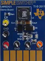
Top View
Bottom View
Figure 1. LMR62421 Demo Board
All trademarks are the property of their respective owners.
SNVA507A – November 2011 – Revised April 2013
Submit Documentation Feedback
Copyright © 2011–2013, Texas Instruments Incorporated
AN-2197 LMR62421 Demo Board
1
�Features
2
Features
•
•
•
•
•
•
•
3
www.ti.com
2.7V to 5.5V Input Voltage Range
12V Output Voltage (default setting)
500mA Output Current from 3.5V input supply
300mA Output Current from 2.7V input supply
Switching Frequency of 1.6 MHz
Low Component Count
PCB size: 27.5mm × 36.9mm
Shutdown Operation
The demo board includes a pull-up resistor R3 to enable the device once VIN has exceeded 1.8V. Use the
EN post to disable the device by pulling this node to GND. A logic signal may be applied to the post to test
startup and shutdown of the device.
4
Adjusting the Output Voltage
The output voltage can be changed from 12V to another voltage by adjusting the feedback resistors using
the following equation:
VOUT = VFB(1 + (R1/R2))
(1)
Where VFB is 1.255V.
5
Feedforward Compensation
The feedforward capacitor CF should be selected to set the compensation zero at approximately 8 kHz.
The value of CF is calculated using:
CF = 1 / (2 × π × 8k × R1)
(2)
The value of CF is calculated after R1 is selected for the output voltage needed for the specific
application.
For more information on component selection and features, see LMR62421 SIMPLE SWITCHER 24Vout,
2.1A Step-Up Voltage Regulator in SOT-23 (SNVS734).
2
AN-2197 LMR62421 Demo Board
SNVA507A – November 2011 – Revised April 2013
Submit Documentation Feedback
Copyright © 2011–2013, Texas Instruments Incorporated
�LMR62421 Demo Board Schematic
www.ti.com
6
LMR62421 Demo Board Schematic
L1
U1
VIN
2
VIN
REN
SW
CF
LMR62421
EN
3
CIN
4
EN
VOUT
D1
6
RFBT
FB
COUT COUT2 CHF
(opt)
5
AGND
PGND
1
RFBB
GND
GND
Figure 2. LMR62421 Demo Board Schematic
Table 1. Bill of Materials LMR62421
ID
Part Number
Type
Size
U1
LMR62421
1.6MHz - SpaceEfficient Boost
6-pin WSON
L1
7447779006
Inductor
D1
B220A-13-F
Diode
Cin
GRM21BR71A106KE51L
Cout
GRM31CR71E106KA12L
Cout2
optional
CF
C0603C221J5GACTU
CHF
Rfbt
Parameters
Vendor
Texas
Instruments
Shielded Inductor,
6.8µH, 2.91A
Wurth
SMA
Schottky, 20V, 2A
Diodes Inc.
Capacitor
0805
Ceramic, 10µF,
10V, X7R
Murata
Capacitor
1206
Ceramic, 10µF,
25V, X7R
Murata
1206
additional output
cap
Capacitor
0603
Ceramic, 220pF,
50V, C0G/NP0
Kemet
GRM188R71H223KA01D
Capacitor
0603
Ceramic, 0.022uF,
50V, X7R
Murata
CRCW060386K6FKEA
Resistor
0603
86.6 kΩ
Vishay
Rfbb
CRCW060310K2FKEA
Resistor
0603
10.2 kΩ
Vishay
Ren
CRCW06031M00JNEA
Resistor
0603
1.0 MegΩ
Vishay
EN
5014
Test Point Loop
Yellow
Keystone
VIN
5010
Test Point Loop
Red
Keystone
VOUT
5013
Test Point Loop
Orange
Keystone
GND
5011
Test Point Loop
Black
Keystone
SNVA507A – November 2011 – Revised April 2013
Submit Documentation Feedback
Copyright © 2011–2013, Texas Instruments Incorporated
AN-2197 LMR62421 Demo Board
3
�Quick Setup Procedures
7
www.ti.com
Quick Setup Procedures
Step 1: Connect a power supply to VIN terminals. VIN range: 2.7V to 5.5V
Step 2: Connect a load to VOUT terminals. IOUT range: 0mA to 500mA
Step 3: Do not allow the EN pin to float or be greater than VIN + 0.3V. EN pin must be connected to VIN by
means R3 for normal operation. Short this to ground to shutdown the part.
Step 4: Turn on VIN with 0A load applied, check VOUT with a voltmeter. Nominal 12V
Step 5: Apply a 500mA load and check VOUT. Nominal 12V
Measurements
Ammeter
A
Ammeter
A
+
VOUT GND
GND
+
-
Electronic
Load
-
8
Power
Supply
VIN
Voltmeter V
V
Voltmeter
Evaluation Board
Figure 3. Efficiency Measurements
Oscilloscope
VOUT
GND
Chf
Figure 4. Voltage Ripple Measurements
4
AN-2197 LMR62421 Demo Board
SNVA507A – November 2011 – Revised April 2013
Submit Documentation Feedback
Copyright © 2011–2013, Texas Instruments Incorporated
�Measurements
www.ti.com
I
I
I
I
I
GND
VOUT
5
6
A
B
C
D
E
F
SPARE
4
VOUT SENSE+
3
VOUT SENSE -
2
VIN SENSE -
1
VIN SENSE+
EN
VIN
I
I
I
I
I
I
I
Figure 5. Edge Connector Schematic
SNVA507A – November 2011 – Revised April 2013
Submit Documentation Feedback
Copyright © 2011–2013, Texas Instruments Incorporated
AN-2197 LMR62421 Demo Board
5
�Typical Performance Characteristics
9
www.ti.com
Typical Performance Characteristics
Efficiency vs. Load Current LMR62421, VOUT = 12V
Load regulation, VOUT = 12V
100
0.100
95
0.075
0.050
85
ERROR [%]
EFFICIENCY [%]
90
80
75
70
65
60
0.025
0.000
-0.025
Vin = 2.7V
Vin = 3.5V
Vin = 5.5V
-0.050
55
-0.075
50
-0.100
0.0
0.1
0.2
0.3
IOUT[A]
0.4
0.5
Output Voltage Ripple and Switching Waveform,
VIN = 2.7, VOUT = 12V, IOUT = 300mA
VOUT
ripple 100 mV/Div
0.0
0.1
0.2
0.3
IOUT[A]
0.4
Output Ripple and Switching Waveform,
VIN = 3.5, VOUT = 12V, IOUT = 500mA
VOUT
ripple
VSW
5V/Div
100 mV/Div
VSW
5V/Div
TIME (200 ns/DIV)
TIME (200 ns/DIV)
Load Transient
VIN = 5.5, VOUT = 12V, IOUT = 50mA to 500mA
Start Up with Enable
VIN = 3.5, VOUT = 12V, IOUT = 500mA
VOUT
ripple
0.5
EN
2V/Div
1V/Div
VSW
2V/Div
IOUT
100 mA/Div
IOUT
200 mA/Div
TIME (1 ms/DIV)
TIME (200 µs/DIV)
6
AN-2197 LMR62421 Demo Board
SNVA507A – November 2011 – Revised April 2013
Submit Documentation Feedback
Copyright © 2011–2013, Texas Instruments Incorporated
�Layout
www.ti.com
10
Layout
Figure 6. Top Layer
Figure 7. Top Overlay
SNVA507A – November 2011 – Revised April 2013
Submit Documentation Feedback
Copyright © 2011–2013, Texas Instruments Incorporated
AN-2197 LMR62421 Demo Board
7
�Layout
www.ti.com
Figure 8. Bottom Layer
Figure 9. Bottom Overlay
8
AN-2197 LMR62421 Demo Board
SNVA507A – November 2011 – Revised April 2013
Submit Documentation Feedback
Copyright © 2011–2013, Texas Instruments Incorporated
�IMPORTANT NOTICE
Texas Instruments Incorporated and its subsidiaries (TI) reserve the right to make corrections, enhancements, improvements and other
changes to its semiconductor products and services per JESD46, latest issue, and to discontinue any product or service per JESD48, latest
issue. Buyers should obtain the latest relevant information before placing orders and should verify that such information is current and
complete. All semiconductor products (also referred to herein as “components”) are sold subject to TI’s terms and conditions of sale
supplied at the time of order acknowledgment.
TI warrants performance of its components to the specifications applicable at the time of sale, in accordance with the warranty in TI’s terms
and conditions of sale of semiconductor products. Testing and other quality control techniques are used to the extent TI deems necessary
to support this warranty. Except where mandated by applicable law, testing of all parameters of each component is not necessarily
performed.
TI assumes no liability for applications assistance or the design of Buyers’ products. Buyers are responsible for their products and
applications using TI components. To minimize the risks associated with Buyers’ products and applications, Buyers should provide
adequate design and operating safeguards.
TI does not warrant or represent that any license, either express or implied, is granted under any patent right, copyright, mask work right, or
other intellectual property right relating to any combination, machine, or process in which TI components or services are used. Information
published by TI regarding third-party products or services does not constitute a license to use such products or services or a warranty or
endorsement thereof. Use of such information may require a license from a third party under the patents or other intellectual property of the
third party, or a license from TI under the patents or other intellectual property of TI.
Reproduction of significant portions of TI information in TI data books or data sheets is permissible only if reproduction is without alteration
and is accompanied by all associated warranties, conditions, limitations, and notices. TI is not responsible or liable for such altered
documentation. Information of third parties may be subject to additional restrictions.
Resale of TI components or services with statements different from or beyond the parameters stated by TI for that component or service
voids all express and any implied warranties for the associated TI component or service and is an unfair and deceptive business practice.
TI is not responsible or liable for any such statements.
Buyer acknowledges and agrees that it is solely responsible for compliance with all legal, regulatory and safety-related requirements
concerning its products, and any use of TI components in its applications, notwithstanding any applications-related information or support
that may be provided by TI. Buyer represents and agrees that it has all the necessary expertise to create and implement safeguards which
anticipate dangerous consequences of failures, monitor failures and their consequences, lessen the likelihood of failures that might cause
harm and take appropriate remedial actions. Buyer will fully indemnify TI and its representatives against any damages arising out of the use
of any TI components in safety-critical applications.
In some cases, TI components may be promoted specifically to facilitate safety-related applications. With such components, TI’s goal is to
help enable customers to design and create their own end-product solutions that meet applicable functional safety standards and
requirements. Nonetheless, such components are subject to these terms.
No TI components are authorized for use in FDA Class III (or similar life-critical medical equipment) unless authorized officers of the parties
have executed a special agreement specifically governing such use.
Only those TI components which TI has specifically designated as military grade or “enhanced plastic” are designed and intended for use in
military/aerospace applications or environments. Buyer acknowledges and agrees that any military or aerospace use of TI components
which have not been so designated is solely at the Buyer's risk, and that Buyer is solely responsible for compliance with all legal and
regulatory requirements in connection with such use.
TI has specifically designated certain components as meeting ISO/TS16949 requirements, mainly for automotive use. In any case of use of
non-designated products, TI will not be responsible for any failure to meet ISO/TS16949.
Products
Applications
Audio
www.ti.com/audio
Automotive and Transportation
www.ti.com/automotive
Amplifiers
amplifier.ti.com
Communications and Telecom
www.ti.com/communications
Data Converters
dataconverter.ti.com
Computers and Peripherals
www.ti.com/computers
DLP® Products
www.dlp.com
Consumer Electronics
www.ti.com/consumer-apps
DSP
dsp.ti.com
Energy and Lighting
www.ti.com/energy
Clocks and Timers
www.ti.com/clocks
Industrial
www.ti.com/industrial
Interface
interface.ti.com
Medical
www.ti.com/medical
Logic
logic.ti.com
Security
www.ti.com/security
Power Mgmt
power.ti.com
Space, Avionics and Defense
www.ti.com/space-avionics-defense
Microcontrollers
microcontroller.ti.com
Video and Imaging
www.ti.com/video
RFID
www.ti-rfid.com
OMAP Applications Processors
www.ti.com/omap
TI E2E Community
e2e.ti.com
Wireless Connectivity
www.ti.com/wirelessconnectivity
Mailing Address: Texas Instruments, Post Office Box 655303, Dallas, Texas 75265
Copyright © 2013, Texas Instruments Incorporated
�


 工商网监
湘ICP备2023018690号
工商网监
湘ICP备2023018690号
