LMS4684
www.ti.com
SNOSAL0C – DECEMBER 2004 – REVISED APRIL 2013
LMS4684 0.5Ω Low-Voltage, Dual SPDT Analog Switch
Check for Samples: LMS4684
FEATURES
DESCRIPTION
•
•
•
•
•
•
The LMS4684 is a low on-resistance, low voltage
dual SPDT (Single-Pole/Double-Throw) analog switch
that operates from a 1.8V to 5.5V supply. The
LMS4684 features a 0.5Ω RON for its NC switch and
0.8Ω RON for its NO switch at a 2.7V supply. The
digital logic inputs are 1.8V logic-compatible with a
2.7V to 3.3V supply and features break-before-make
switching action.
1
2
NC Switch RON 0.5Ω max @ 2.7V
NO Switch RON 0.8Ω max @ 2.7V
5 nA (typ) Supply Current TA = 25°C
1.8 to 5.5V Single Supply Operation
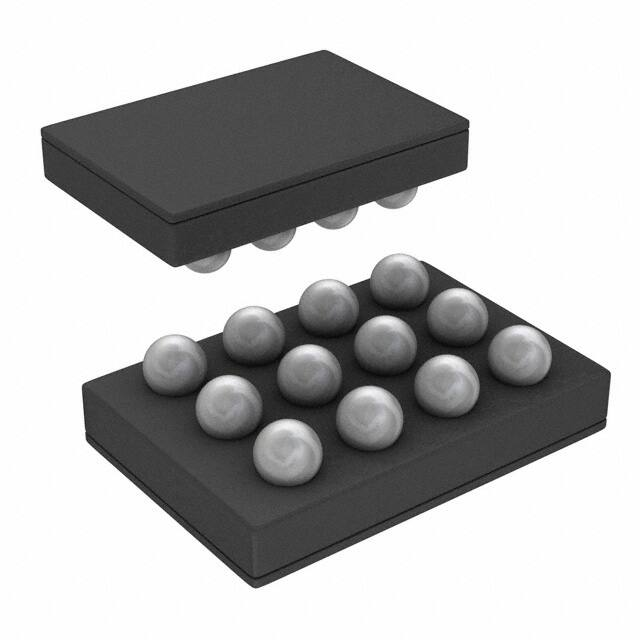
12-Bump DSBGA Package
WSON-10 Package, 3x4mm
The LMS4684 is available in the 12-bump DSBGA
and the 10-lead WSON miniature packages. These
PCB real estate saving packages offer extreme
performance while saving money with small
footprints.
APPLICATIONS
•
•
•
•
•
Power Routing
Battery-Operated Equipment
Communications Circuits
Modems
Cell Phones
Connection Diagram
V
+
1
NO1
2
COM1
3
IN1
4
10
NC1
5
9
COM2
8
IN2
7
NC2
6
COM1
IN1
NC1
A3
B3
C3
D3
A2
B2
C2
D2
A1
B1
C1
D1
NO2
COM2
IN2
NC2
NO2
+
GND
NO1
V
GND
GND
Center Bumps B2 and C2 are Not Electrically Connected
Exposed pad on back of package needs to be connected to pin 6 on
the board
Figure 1. 10-WSON Package-Top View
Figure 2. 12-Bump DSBGA Package-Top View
(Bumped Side Down)
1
2
Please be aware that an important notice concerning availability, standard warranty, and use in critical applications of
Texas Instruments semiconductor products and disclaimers thereto appears at the end of this data sheet.
All trademarks are the property of their respective owners.
PRODUCTION DATA information is current as of publication date.
Products conform to specifications per the terms of the Texas
Instruments standard warranty. Production processing does not
necessarily include testing of all parameters.
Copyright © 2004–2013, Texas Instruments Incorporated
�LMS4684
SNOSAL0C – DECEMBER 2004 – REVISED APRIL 2013
www.ti.com
SCHEMATIC DIAGRAM
+
1
10
NO2
NO1
2
9
COM2
COM1
3
8
IN2
IN1
4
7
NC2
NC1
5
6
GND
V
IN
NO
NC
0
Off
On
1
On
Off
Switches shown for Logic "0" input
PIN DESCRIPTIONS
Name
Pin ID
Description
WSON
DSBGA
NC
5, 7
D3, D1
Analog switch normally closed terminal
IN
4, 8
C3, C1
Digital control input
COM
3, 9
B3, B1
Analog switch common terminal
NO
2, 10
A3, A1
Analog switch normally open terminal
V+
1
A2
Positive supply voltage
GND
6
D2
Ground
B2, C2
Not electrically connected. Can be used to help dissipate heat by connecting to GND
pin.
These devices have limited built-in ESD protection. The leads should be shorted together or the device placed in conductive foam
during storage or handling to prevent electrostatic damage to the MOS gates.
ABSOLUTE MAXIMUM RATINGS
(1) (2) (3)
V+
−0.3V to 6.0V
−0.3V to 6.0V
IN
−0.3V to (V+ + 0.3V)
COM, NO, NC
Continuous Switch Current
ESD Tolerance
(4)
±400 mA
Human Body Model
Machine Model
(1)
(2)
(3)
(4)
(5)
2
200V
−65°C to 150°C
Storage Temperature Range
Junction Temperature
2000V
(5)
150°C Max
Absolute Maximum Ratings indicate limits beyond which damage to the device may occur. Operating Ratings indicate conditions for
which the device is intended to be functional, but specific performance is not guaranteed.
All voltages are with respect to GND, unless otherwise specified.
If Military/Aerospace specified devices are required, please contact the Texas Instruments Sales Office/ Distributors for availability and
specifications.
Human body model: 1.5 kΩ in series with 100 pF. Machine model, 0Ω in series with 200 pF.
The maximum power dissipation is a function of TJ(max), θJA and TA.
Submit Documentation Feedback
Copyright © 2004–2013, Texas Instruments Incorporated
Product Folder Links: LMS4684
�LMS4684
www.ti.com
SNOSAL0C – DECEMBER 2004 – REVISED APRIL 2013
OPERATING RATINGS
Nominal Supply Voltage
1.8V to 5.5V
−0.3V to 5.5V
IN Voltage (regardless of supply)
−40°C to 85°C
Temperature Range
(1)
(2)
Absolute Maximum Ratings indicate limits beyond which damage to the device may occur. Operating Ratings indicate conditions for
which the device is intended to be functional, but specific performance is not guaranteed.
All voltages are with respect to GND, unless otherwise specified.
PACKAGE THERMAL RESISTANCE
Package
θJ-A
WSON-10
43°C / W
DSBGA-12
57°C / W
ELECTRICAL CHARACTERISTICS
Unless otherwise specified, V+ = 2.7 to 3.3V, VIH = 1.4V, VIL = 0.5V. Typical values are measured at 3V, and TJ = 25°C.
Boldface limits apply at temperature extremes.
Symbol
VNO, VNC, VCOM
RON
(NC)
RON
(NO)
Parameter
Conditions
Analog Signal Range
NC On-Resistance
(1)
On-Resistance Match
Between Channels (1),
RFLAT(NO)
INO(OFF) or INC(OFF)
ICOM (ON)
Max
Units
+
V
V
V+ = 2.7V, ICOM = 100 mA,
VNC =0 to V+
0.3
0.5
Ω
V+ = 2.7V, ICOM = 100 mA,
VNO =0 to V+
0.45
0.8
Ω
1.11
60
mΩ
WSON
TJ = -40°C to
85°C
0.1
0.25
DSBGA
TJ = -40°C to
85°C
0.1
0.25
0.18
0.35
+
(2)
V = 2.7V, ICOM = 100 mA,
VNC or VNO =1.5V
+
RFLAT(NC)
Typ
0
(1)
NO On-Resistance
ΔRON
Min
NC-On-Resistance
Flatness (3)
V = 2.7V,
ICOM = 100 mA,
VNC = 0 to V+
NO On-Resistance
Flatness (3)
V+ = 2.7V, ICOM = 100 mA,
VNO = 0 to V+
NO or NC Off Leakage
Current
V+ = 3.3V, VNO or VNC = 3V,
0.3V; VCOM = 0.3V, 3V
COM On Leakage Current
V+ = 3.3V, VNO or VNC = 3V,
0.3V, or floating; VCOM = 3V, or
floating
Ω
−1
0.014
1
−10
10
−2
2
−20
20
Ω
nA
nA
Dynamic Characteristics
tON
Turn-On Time
V+ = 2.7V, VNO or VNC = 1.5V;
RL = 50Ω; CL = 35 pF;
38
tOFF
Turn-Off Time
V+ = 2.7V, VNO or VNC = 1.5V;
RL = 50Ω; CL = 35 pF;
22
tBBM
Break-Before-Make Delay
V+ = 2.7V, VNO or VNC = 1.5V;
RL = 50Ω; CL = 35 pF;
Charge Injection
Q
VISO
Off-Isolation
VCT
Crosstalk
(4)
60
70
40
50
2
ns
ns
15
ns
COM = 0; RS = 0; CL= 1 nF;
200
pC
RL = 50Ω; CL= 5 pF; f = 100 kHz
-68
dB
-72
dB
Digital I/O
(1)
(2)
(3)
(4)
VIH
Input Logic High
VIL
Input Logic Low
1.4
V
0.5
V
Guaranteed by design.
ΔRON is equal to the difference between NC1/NC2 RON or NO1/NO2 RON at a specified voltage.
Flatness is defined as the difference between the maximum and minimum value of on-resistance as measured over the specified analog
signal ranges.
Off-isolation = 20 log10(VCOM/ VNO), where VCOM = output, VNO = input switch off.
Submit Documentation Feedback
Copyright © 2004–2013, Texas Instruments Incorporated
Product Folder Links: LMS4684
3
�LMS4684
SNOSAL0C – DECEMBER 2004 – REVISED APRIL 2013
www.ti.com
ELECTRICAL CHARACTERISTICS (continued)
Unless otherwise specified, V+ = 2.7 to 3.3V, VIH = 1.4V, VIL = 0.5V. Typical values are measured at 3V, and TJ = 25°C.
Boldface limits apply at temperature extremes.
Symbol
IIN
Parameter
Conditions
Min
VIN = 0 or V+
IN Input Leakage Current
Typ
−1
Max
Units
1
μA
Power Supply
V+
Power-Supply Range
I+
Supply Current
1.8
5.5
V+ = 5.5V
5
V
nA
PARAMETRIC MEASUREMENT INFORMATION
V
+
0.047PF
V
+
NO
VIN
LOGIC
INPUT
COM
RL
50:
50%
VIL
VOUT
or NC
VIH
tOFF
CL
100pF
VOUT
IN
0.9 x VOUT
SWITCH
OUPUT
GND
0.9 x VOUT
0
LOGIC
INPUT
tON
CL INCLUDES FIXTURE AND STRAY CAPACITANCE
Figure 3. tON / tOFF Time
+
V
0.047PF
V+
LOGIC
INPUT
NC
VIN
COM
VOUT
VIH
50%
VIL
NO
RL
50:
CL
100pF
IN
GND
LOGIC
INPUT
0.9 x VOUT
tD
CL INCLUDES FIXTURE AND STRAY CAPACITANCE
Figure 4. Break-Before Make Delay
4
Submit Documentation Feedback
Copyright © 2004–2013, Texas Instruments Incorporated
Product Folder Links: LMS4684
�LMS4684
www.ti.com
SNOSAL0C – DECEMBER 2004 – REVISED APRIL 2013
+
V
0.047PF
VOUT
V+
VOUT
RGEN
COM
VOUT
NC
or NO
IN
CL
+
OFF
OFF
VGEN
ON
GND
IN
ON
OFF
OFF
IN
VIL to VIH
Q=(
VOUT)(CL)
Figure 5. Charge Injection
0.047 PF
V
+
V
+
COM
IN
CAPACITANCE
METER
VIL
or
VIH
NC or
NO
f = 1 MHz
GND
Figure 6. Channel Capacitance
Submit Documentation Feedback
Copyright © 2004–2013, Texas Instruments Incorporated
Product Folder Links: LMS4684
5
�LMS4684
SNOSAL0C – DECEMBER 2004 – REVISED APRIL 2013
www.ti.com
TYPICAL PERFORMANCE CHARACTERISTICS
NO ON Resistance
vs.
COM Voltage
3.0
NC ON Resistance
vs.
COM Voltage
2.50
+
V = 1.8V
2.5
2.00
+
1.75
1.5
RON (:)
V = 2.0V
2.0
RON (:)
VS = 1.8V
2.25
+
V = 2.3V
+
1.0
V = 5.0V
+
VS = 2.0V
1.50
1.25
0.75
V = 2.5V
+
V = 3.0V
VS = 5.0V
VS = 2.3V
1.00
VS = 2.5V
VS = 3.0V
0.50
0.5
0.25
0.0
1
0
3
2
0.00
0.0
5
4
3.0
4.0
Figure 7.
Figure 8.
Logic Threshold Voltage
vs.
Supply Voltage
Turn-on / Turn-off Times
vs.
Temperature
50
5.0
tON (ns)
45
40
1.5
35
VIN RISING
tON , tOFF (ns)
LOGIC THRESHOLD VOLTAGE (V)
2.0
VCOM (V)
2
1
VIN FALLING
30
tOFF (ns)
25
20
V+ = 3V
15
0.5
CL = 100 pF
10
RL = 50:
5
0
0
1
2
3
4
5
6
0
-40
-15
10
35
60
85
TEMPERATURE
VSUPPLY (V)
Figure 9.
6
1.0
VCOM (V)
Figure 10.
Submit Documentation Feedback
Copyright © 2004–2013, Texas Instruments Incorporated
Product Folder Links: LMS4684
�LMS4684
www.ti.com
SNOSAL0C – DECEMBER 2004 – REVISED APRIL 2013
TYPICAL PERFORMANCE CHARACTERISTICS (continued)
Charge Injection
vs.
COM Voltage
NC On-Resistance
vs.
COM Voltage
0.30
500
+
V = 5V
0.28
300
0.24
100
-100
TA = +25ºC
0.22
RON (:)
Q (pC)
TA = +85ºC
0.26
0.20
0.18
-300
0.16
0.14
-500
TA = -40ºC
0.12
0.10
-700
0
1
2
3
0
6
5
4
2
1
3
4
VCOM (V)
VCOM (V)
Figure 11.
Figure 12.
NC On-Resistance
vs.
COM Voltage
NO On-Resistance
vs.
COM Voltage
0.35
0.60
+
V = 3V
+
V = 3V
TA = +85ºC
0.55
0.30
5
0.50
TA = +85ºC
0.20
TA = -40ºC
0.40
RON (:)
RON (:)
0.45
TA = +25ºC
0.25
TA = +25ºC
0.35
0.30
TA = -40ºC
0.25
0.15
0.20
0.15
0.10
0.10
0
0.5
1
1.5
2
3
2.5
0
0.5
1
1.5
VCOM (V)
VCOM (V)
Figure 13.
Figure 14.
2
2.5
3
NO On-Resistance
vs.
COM Voltage
0.40
0.35 TA = +85ºC
RON (:)
0.30
TA = +25ºC
0.25
0.20
TA = -40ºC
0.15
+
V = 5V
0.10
0
1
2
3
4
5
VCOM (V)
Figure 15.
Submit Documentation Feedback
Copyright © 2004–2013, Texas Instruments Incorporated
Product Folder Links: LMS4684
7
�LMS4684
SNOSAL0C – DECEMBER 2004 – REVISED APRIL 2013
www.ti.com
FUNCTIONAL DESCRIPTION
The LMS4684 is a low voltage dual, extremely low On-Resistance analog switch that can operate over a supply
voltage range of 1.8V to 5.5V. The LMS4684 has been fully characterized to operate in applications with 3V
nominal supply voltage and features very low on resistance and fast Turn-Off and Turn-On times with breakbefore-make switching.
The switch operates asymmetrically; one terminal is normally closed (NC) and the other terminal normally open
(NO).
Both NC and NO terminals are connected to a common terminal (COM). This configuration is ideal for
applications with asymmetric loads such as speaker handsets and internal speakers.
Applications Information
ANALOG INPUT SIGNAL
Analog input signals can range from GND to V+ and are passed through the switch with very little change. Each
switch is bidirectional so any pin can be an input or output.
Exercise care when making connection to an inductive load, such as a motor. As is true with any analog switch
used with an inductive load, the back emf produced when the switch is turned off can damage the LMS4684 by
electrical overstress. For such applications, a diode should be connected across the motor to prevent damage to
the switch, as indicated in Figure 16. Be sure the diode has adequate current carrying capabilities.
V
+
0.047PF
V
+
Protection
Diode
COM
NC
or NO
Motor or
inductive
load
+
VIN
GND
VOUT
IN
VIL to VIH
Figure 16. Inductive Load Over-Voltage Protection
DIGITAL CONTROL INPUTS
The IN pin can be driven to 5.5V regardless of the voltage level of the supply pin V+. For example, if the
LMS4684 is operated with a supply of 2V, the digital control input could still be driven to 5V. Power consumption
is increased when the control pin is driven rail-to-rail.
SUPPLY VOLTAGE
It is good general practice to first apply the supply voltage to a CMOS device before sriving any other pins. This
is also true for the LMS4684 analog switch, which is a CMOS device.
However, if it is necessary to have an analog signal applied before the supply voltage is applied and the analog
signal source is not limited to 20 mA max, a diode connected between the supply voltage and the V+ pin as
shown in Figure 17 will provide input protection. This will limit the max analog voltage to a diode drop below V+.
This diode, D1, will also provide protection against some over voltage situations.
8
Submit Documentation Feedback
Copyright © 2004–2013, Texas Instruments Incorporated
Product Folder Links: LMS4684
�LMS4684
www.ti.com
SNOSAL0C – DECEMBER 2004 – REVISED APRIL 2013
It is also good practice to provide adequate supply bypassing to all analog circuits. We recommend a that
minimum bypass capacitor value of 0.047µF be provided for the LMS4684. An inadequate bypass capacitor can
lead to excessive supply current.
SUPPLY VOLTAGE
D1
0.047 PF
NO
COM
ANALOG
INPUT
SIGNAL
GND
Figure 17. Input Over Voltage Protection Circuitry
OFF-ISOLATION
Analog switches are composed of FETs (field Effect Transistors). The channel resistance is low when the pass
transistors are "on" and that resistance is high when the pass transistors are "off". However, when the pass
transistors are "off", the source to drain capacitance of the pass transistors will pass some energy. This
capacitance is inversely proportional to the switch "on" resistance, so a switch with a low "on" resistance may not
be suitable for some high frequency applications.
Figure 18 shows the equivalent circuit of an analog switch. Unless the load impedance after the switch is
relatively low, the switch capacitance will couple excessive energy across the "open" switch at higher
frequencies, degrading off isolation performance. Off Isolation of the LMS4684 is specified with a 50Ω load.
Higher load impedances will degrade off isolation performance compared with what is specified.
NO or
NC
RON
COM
CS
Figure 18. Equivalent Circuit of an Analog Switch
Off isolation may be improved by decreasing the LMS4684 load impedance below 50Ω. When doing this, be sure
that the LMS4684 maximum current rating is not exceeded. Also, decreasing the load impedance too much can
result in excessive signal distortion because the channel resistance variation with input signal voltage would then
be a greater percentage of the load impedance.
If it is desired to extend the usable bandwidth of the LMS4684 while maintaining reasonable off-isolation is
through the use of the circuit of Figure 19.
Submit Documentation Feedback
Copyright © 2004–2013, Texas Instruments Incorporated
Product Folder Links: LMS4684
9
�LMS4684
SNOSAL0C – DECEMBER 2004 – REVISED APRIL 2013
www.ti.com
V
+
0.047 PF
+
V
NO
VIN
COM
NC
GND
Figure 19. Using the LMS4684 at higher frequencies
PCB LAYOUT AND THERMAL CONSIDERATIONS
Both the WSON and DSBGA packages offer enhanced board real estate savings because of their small
footprints. These tiny packages are capable of handling high continuous currents because of the advanced
package thermal handling capabilities.
The WSON package has the exposed die attach pad internally connected to the internal circuit GND. When this
pad is soldered to copper on the PCB board according to Application Note AN-1187, the full thermal capability of
the WSON package can be achieved without additional bulky heat sinks to dissipate the heat generated. The
DSBGA package has a similar capability to dissipate heat through Bumps B2 and C2, which are not electrically
connected. To enhance heat dissipation of the DSBGA package B2 and C2 could be connected to the GND pin
through copper traces on the board.
See Application Note AN-1112 for DSBGA package considerations.
10
Submit Documentation Feedback
Copyright © 2004–2013, Texas Instruments Incorporated
Product Folder Links: LMS4684
�LMS4684
www.ti.com
SNOSAL0C – DECEMBER 2004 – REVISED APRIL 2013
REVISION HISTORY
Changes from Revision B (April 2013) to Revision C
•
Page
Changed layout of National Data Sheet to TI format .......................................................................................................... 10
Submit Documentation Feedback
Copyright © 2004–2013, Texas Instruments Incorporated
Product Folder Links: LMS4684
11
�PACKAGE OPTION ADDENDUM
www.ti.com
10-Dec-2020
PACKAGING INFORMATION
Orderable Device
Status
(1)
Package Type Package Pins Package
Drawing
Qty
Eco Plan
(2)
Lead finish/
Ball material
MSL Peak Temp
Op Temp (°C)
Device Marking
(3)
(4/5)
(6)
LMS4684ITL/NOPB
ACTIVE
DSBGA
YZR
12
250
RoHS & Green
SNAGCU
Level-1-260C-UNLIM
-40 to 85
F09A
LMS4684ITLX/NOPB
ACTIVE
DSBGA
YZR
12
3000
RoHS & Green
SNAGCU
Level-1-260C-UNLIM
-40 to 85
F09A
LMS4684LD/NOPB
ACTIVE
WSON
NGZ
10
1000
RoHS & Green
SN
Level-3-260C-168 HR
-40 to 85
L4684
(1)
The marketing status values are defined as follows:
ACTIVE: Product device recommended for new designs.
LIFEBUY: TI has announced that the device will be discontinued, and a lifetime-buy period is in effect.
NRND: Not recommended for new designs. Device is in production to support existing customers, but TI does not recommend using this part in a new design.
PREVIEW: Device has been announced but is not in production. Samples may or may not be available.
OBSOLETE: TI has discontinued the production of the device.
(2)
RoHS: TI defines "RoHS" to mean semiconductor products that are compliant with the current EU RoHS requirements for all 10 RoHS substances, including the requirement that RoHS substance
do not exceed 0.1% by weight in homogeneous materials. Where designed to be soldered at high temperatures, "RoHS" products are suitable for use in specified lead-free processes. TI may
reference these types of products as "Pb-Free".
RoHS Exempt: TI defines "RoHS Exempt" to mean products that contain lead but are compliant with EU RoHS pursuant to a specific EU RoHS exemption.
Green: TI defines "Green" to mean the content of Chlorine (Cl) and Bromine (Br) based flame retardants meet JS709B low halogen requirements of


 工商网监
湘ICP备2023018690号
工商网监
湘ICP备2023018690号
