LMS485
October 12, 2011
5V Low Power RS-485 / RS-422 Differential Bus Transceiver
General Description
Features
The LMS485 is a low power differential bus/line transceiver
designed for high speed bidirectional data communication on
multipoint bus transmission lines. It is designed for balanced
transmission lines. It meets ANSI Standards TIA/EIA RS422B, TIA/EIA RS485-A and ITU recommendation and V.11 and
X.27. The LMS485 combines a TRI-STATE® differential line
driver and differential input receiver, both of which operate
from a single 5.0V power supply. The driver and receiver have
an active high and active low, respectively, that can be externally connected to function as a direction control. The driver
and receiver differential inputs are internally connected to
form differential input/output (I/O) bus ports that are designed
to offer minimum loading to bus whenever the driver is disabled or when VCC = 0V. These ports feature wide positive
and negative common mode voltage ranges, making the device suitable for multipoint applications in noisy environments.
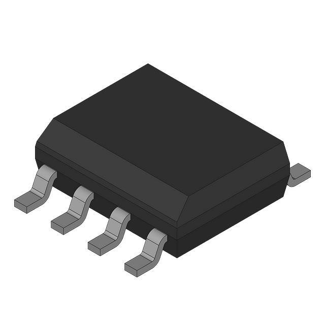
The LMS485 is available in a 8-Pin SOIC and 8-Pin DIP packages. It is a drop-in socket replacement to Maxim’s MAX485
■
■
■
■
■
■
■
■
■
■
■
Meet ANSI standard RS-485-A and RS-422-B
Data rate 2.5 Mbps
Single supply voltage operation, 5V
Thermal shutdown protection
Short circuit protection
Low power BiCMOS
Allows up to 32 transceivers on the bus
Open circuit fail-safe for receiver
Extended operating temperature range −40°C to 85°C
Drop-in replacement to MAX485
Available in 8-pin SOIC and 8-Pin DIP package
Applications
■
■
■
■
■
■
■
■
Low power RS-485 systems
Network hubs, bridges, and routers
Point of sales equipment (ATM, barcode scanners,…)
Local area networks (LAN)
Integrated service digital network (ISDN)
Industrial programmable logic controllers
High speed parallel and serial applications
Multipoint applications with noisy environment
Typical Application
20062601
A Typical multipoint application is shown in the above figure. Terminating resistors, RT, are typically required but only located at the two ends of the cable.
Pull up and pull down resistors maybe required at the end of the bus to provide failsafe biasing. The biasing resistors provide a bias to the cable when all
drivers are in TRI-STATE, See National Application Note, AN-847 for further information.
TRI-STATE® is a registered trademark of National Semiconductor Corporation.
© 2011 National Semiconductor Corporation
200626
200626 Version 3 Revision 1
www.national.com
Print Date/Time: 2011/10/12 10:59:46
LMS485 5V Low Power RS-485 / RS-422 Differential Bus Transceiver
OBSOLETE
�LMS485
Connection Diagram
8-Pin SOIC / DIP
20062602
Top View
Truth Table
DRIVER SECTION
RE
DE
DI
A
X
H
H
H
B
L
X
H
L
L
H
X
L
X
Z
Z
RECEIVER SECTION
RE
DE
A-B
RO
L
L
H
L
L
≥ +0.2V
≤ −0.2V
H
X
X
Z
L
L
OPEN *
H
L
Note: * = Non Terminated, Open Input only
X = Irrelevant
Z = TRI-STATE
H = High level
L = Low level
Pin Descriptions
Pin #
I/O
Name
Function
1
O
RO
Receiver Output: If A > B by 200 mV, RO will be high; If A < B by 200mV, RO will be low. RO will be
high also if the inputs (A and B) are open (non-terminated)
2
I
RE
Receiver Output Enable: RO is enabled when RE is low; RO is in TRI-STATE when RE is high
3
I
DE
Driver Output Enable: The driver outputs (A and B) are enabled when DE is high; they are in TRISTATE when DE is low. Pins A and B also function as the receiver input pins (see below)
4
I
DI
Driver Input: A low on DI forces A low and B high while a high on DI forces A high and B low when
the driver is enabled
5
N/A
GND
Ground
6
I/O
A
Non-inverting Driver Output and Receiver Input pin. Driver Output levels conform to RS-485 signaling
levels
7
I/O
B
Inverting Driver Output and Receiver Input pin. Driver Output levels conform to RS-485 signaling
levels
8
N/A
VCC
Power Supply: 4.75V ≤ VCC ≤ 5.25V
www.national.com
2
200626 Version 3 Revision 1
Print Date/Time: 2011/10/12 10:59:46
�Package
Part Number
LMS485CM
8-Pin SOIC
LMS485CMX
LMS485IM
LMS485IMX
8-Pin DIP
Package Marking
LMS485CM
LMS485IM
Transport Media
2.5k Units Tape and Reel
95 Units/Rail
M08A
2.5k Units Tape and Reel
LMS485CNA
LMS485CNA
40 Units/Rail
LMS485INA
LMS485INA
40 Units/Rail
3
200626 Version 3 Revision 1
NSC Drawing
95 Units/Rail
Print Date/Time: 2011/10/12 10:59:46
N08E
www.national.com
LMS485
Ordering Information
�LMS485
Absolute Maximum Ratings (Note 1)
Operating Ratings
If Military/Aerospace specified devices are required,
please contact the National Semiconductor Sales Office/
Distributors for availability and specifications.
Supply Voltage, VCC (Note 2)
Input Voltage, VIN (DI, DE, or RE)
Voltage Range at Any Bus Terminal
(AB)
Receiver Outputs
Supply Voltage, VCC
Voltage at any Bus Terminal
(Separately or Common Mode)
VIN or VIC
High-Level Input Voltage, VIH
(Note 5)
Low-Level Input Voltage, VIL
(Note 5)
Differential Input Voltage, VID
(Note 6)
High-Level Output
Driver, IOH
7V
−0.3V to VCC + 0.3V
−7V to 12V
−0.3V to VCC + 0.3V
Package Thermal Impedance, θJA
SOIC
DIP
Junction Temperature (Note 3)
Operating Free-Air Temperature
Range, TA
Commercial
Industrial
Storage Temperature Range
Soldering Information
Infrared or Convection (20 sec.)
Lead Temperature (4 sec.)
ESD Rating (Note 4)
125°C/W
88°C/W
150°C
Min Nom Max
4.75 5.0 5.25
−7
12
2
V
Receiver, IOH
Low-Level Output
Driver, IOL
Receiver, IOL
0°C to 70°C
−40°C to 85°C
−65°C to 150°C
V
V
0.8
V
±12
V
−15
0
−42
mA
80
26
mA
mA
mA
235°C
260°C
7kV
Electrical Characteristics
Over recommended ranges of supply voltage and operating free-air temperature (unless otherwise noted)
Symbol
Parameter
Conditions
Min
Typ
Max
Units
5.25
V
Driver Section
| VOD1 |
Differential Output Voltage
R = ∞ (Figure 1)
| VOD2 |
Differential Output Voltage
R = 50Ω (Figure 1) ,RS-422
2.0
R = 27Ω (Figure 1) ,RS-485
1.5
V
5.0
ΔVOD
Change in Magnitude of Driver R = 27Ω or 50Ω
Differential Output Voltage for (Figure 1 ), (Note 7)
Complementary Output States
0.2
V
VOC
Common-Mode Output Voltage R = 27Ω or 50Ω (Figure 1)
3.0
V
ΔVOC
Change in Magnitude of Driver R = 27Ω or 50Ω
Common-Mode Output Voltage (Figure 1), (Note 7)
for Complementary Output
States
0.2
V
VIH
CMOS Inout Logic Threshold
High
DE, DI, RE
VIL
CMOS Input Logic Threshold
Low
DE, DI, RE
0.8
IIN1
Logic Input Current
DE, DI, RE
±2
μA
DE = 0V, VCC = 0V or 5.25V
VIN = 12V
1.0
mA
VIN = − 7V
−0.8
2.0
V
V
Receiver Section
IIN2
Input Current (A, B)
VTH
Differential Input Threshold
Voltage
−7V ≤ VCM ≤ + 12V
ΔVTH
Input Hysteresis Voltage
(VTH+ − VTH−)
VCM = 0
VOH
CMOS High-level Output
Voltage
IOH = −4mA, VID = 200mV
VOL
CMOS Low-level
IOL = 4mA, VID = −200mV
www.national.com
−0.2
95
Print Date/Time: 2011/10/12 10:59:46
V
mV
3.5
4
200626 Version 3 Revision 1
+0.2
V
0.40
V
�Parameter
Conditions
IOZR
Tristate Output Leakage
Current
0.4V ≤ VO ≤ + 2.4V
RIN
Input Resistance
− 7V ≤ VCM≤+12V
Min
Typ
Max
Units
±1
μA
12
kΩ
Power Supply Current
DE = VCC, RE = GND or VCC
Supply Current
IOSD1
Driver Short-circuit Output
Current
VO = high, −7V ≤ VCM ≤ + 12V
(Note 8)
35
250
mA
IOSD2
Driver Short-circuit Output
Current
VO = low, − 7V ≤VCM ≤ + 12V
(Note 8)
35
250
mA
IOSR
Receiver Short-circuit Output
Current
0 V ≤VO ≤ VCC
7
95
mA
10
35
60
nS
5
10
nS
8
40
nS
DE = 0V, RE = GND or VCC
320
500
315
400
μA
ICC
Switching Characteristics
Driver
TPLH,
TPHL
Propagation Delay Input to
Output
RL = 54Ω, CL = 100pF
(Figure 3, Figure 7)
TSKEW
Driver Output Skew
RL = 54Ω, CL = 100 pF
(Figure 3, Figure 7)
TR,
TF
Driver Rise and Fall Time
RL = 54Ω, CL = 100 pF
(Figure 3, Figure 7)
TZH,
TZL
Driver Enable to Ouput Valid
Time
CL = 100 pF, RL = 500Ω
(Figure 4, Figure 8)
25
70
nS
THZ,
TLZ
Driver Output Disable Time
CL = 15 pF, RL = 500Ω
(Figure 4, Figure 8)
30
70
nS
TPLH,
TPHL
Propagation Delay Input to
Output
RL = 54Ω, CL = 100 pF
(Figure 5, Figure 7)
50
200
nS
TSKEW
Receiver Output Skew
RL = 54Ω, CL = 100 pF
(Figure 5, Figure 7)
5
TZH,
TZL
Receiver Enable Time
CL = 15 pF, RL = 1 kΩ
(Figure 6, Figure 10)
20
50
20
50
3
Receiver
20
Receiver Disable Time
FMAX
Maximum Data Rate
2.5
nS
nS
nS
Mbps
Note 1: Absolute Maximum Ratings indicate limits beyond which damage to the device may occur. Operating Ratings indicate conditions for which the device is
intended to be functional, but specific performance is not guaranteed. For guaranteed specifications and the test conditions, see the Electrical Characteristics
Note 2: All voltage values, except differential I/O bus voltage, are with respect to network ground terminal.
Note 3: The maximum power dissipation is a function of TJ(MAX), θJA, and TA. The maximum allowable power dissipation at any ambient temperature is PD = (TJ
(MAX) - TA)/θJA. All numbers apply for packages soldered directly into a PC board.
Note 4: ESD rating based upon human body model, 100pF discharged through 1.5kΩ.
Note 5: Voltage limits apply to DI, DE, RE pins.
Note 6: Differential input/output bus voltage is measured at the non-inverting terminal A with respect to the inverting terminal B.
Note 7: |ΔVOD| and |ΔVOC| are changes in magnitude of VOD and VOC, respectively when the input changes from high to low levels.
Note 8: Peak current
5
200626 Version 3 Revision 1
Print Date/Time: 2011/10/12 10:59:46
www.national.com
LMS485
Symbol
�LMS485
Typical Performance Characteristics
Output Current vs. Receiver Output Low Voltage
Output Current vs. Receiver Output High Voltage
20062614
20062613
Receiver Output High Voltage vs. Temperature
Receiver Output Low-Voltage vs. Temperature
20062616
20062615
Driver Output Current vs. Differential Output Voltage
Driver Differential Output Voltage vs. Temperature
20062618
20062617
www.national.com
6
200626 Version 3 Revision 1
Print Date/Time: 2011/10/12 10:59:46
�Output Current vs. Driver Output High Voltage
20062619
20062620
Supply Current vs. Temperature
20062621
7
200626 Version 3 Revision 1
Print Date/Time: 2011/10/12 10:59:46
www.national.com
LMS485
Output Current vs. Driver Output Low Voltage
�LMS485
Parameter Measuring Information
20062603
FIGURE 1. Test Circuit for VOD and VOC
20062604
FIGURE 2. Test Circuit for VOD3
20062605
FIGURE 3. Test Circuit for Driver Propagation Delay
20062606
FIGURE 4. Test Circuit for Driver Enable / Disable
www.national.com
8
200626 Version 3 Revision 1
Print Date/Time: 2011/10/12 10:59:46
�LMS485
20062607
FIGURE 5. Test Circuit for Receiver Propagation Delay
20062608
FIGURE 6. Test Circuit for Receiver Enable / Disable
9
200626 Version 3 Revision 1
Print Date/Time: 2011/10/12 10:59:46
www.national.com
�LMS485
Switching Characteristics
20062611
FIGURE 9. Receiver Propagation Delay
20062609
FIGURE 7. Driver Propagation Delay, Rise / Fall Time
20062612
FIGURE 10. Receiver Enable / Disable Time
20062610
FIGURE 8. Driver Enable / Disable Time
www.national.com
10
200626 Version 3 Revision 1
Print Date/Time: 2011/10/12 10:59:46
�POWER LINE NOISE FILTERING
A factor to consider in designing power and ground is noise
filtering. A noise filtering circuit is designed to prevent noise
generated by the integrated circuit (IC) as well as noise entering the IC from other devices. A common filtering method
is to place by-pass capacitors (Cbp) between the power and
ground lines.
Placing a by-pass capacitor (Cbp) with the correct value at the
proper location solves many power supply noise problems.
Choosing the correct capacitor value is based upon the desired noise filtering range. Since capacitors are not ideal, they
20062622
FIGURE 11. Placement of by-pass Capacitors, Cbp
11
200626 Version 3 Revision 1
Print Date/Time: 2011/10/12 10:59:46
www.national.com
LMS485
may act more like inductors or resistors over a specific frequency range. Thus, many times two by-pass capacitors may
be used to filter a wider bandwidth of noise. It is highly recommended to place a larger capacitor, such as 10μF, between the power supply pin and ground to filter out low
frequencies and a 0.1μF to filter out high frequencies.
By-pass capacitors must be mounted as close as possible to
the IC to be effective. Long leads produce higher impedance
at higher frequencies due to stray inductance. Thus, this will
reduce the by-pass capacitor’s effectiveness. Surface mounted chip capacitors are the best solution because they have
lower inductance.
Application Information
�LMS485
Physical Dimensions inches (millimeters) unless otherwise noted
8-Pin SOIC
NS Package Number M08A
8-Pin DIP
NS Package Number N08E
www.national.com
12
200626 Version 3 Revision 1
Print Date/Time: 2011/10/12 10:59:46
�LMS485
Notes
13
200626 Version 3 Revision 1
Print Date/Time: 2011/10/12 10:59:46
www.national.com
�LMS485 5V Low Power RS-485 / RS-422 Differential Bus Transceiver
Notes
For more National Semiconductor product information and proven design tools, visit the following Web sites at:
www.national.com
Products
Design Support
Amplifiers
www.national.com/amplifiers
WEBENCH® Tools
www.national.com/webench
Audio
www.national.com/audio
App Notes
www.national.com/appnotes
Clock and Timing
www.national.com/timing
Reference Designs
www.national.com/refdesigns
Data Converters
www.national.com/adc
Samples
www.national.com/samples
Interface
www.national.com/interface
Eval Boards
www.national.com/evalboards
LVDS
www.national.com/lvds
Packaging
www.national.com/packaging
Power Management
www.national.com/power
Green Compliance
www.national.com/quality/green
Switching Regulators
www.national.com/switchers
Distributors
www.national.com/contacts
LDOs
www.national.com/ldo
Quality and Reliability
www.national.com/quality
LED Lighting
www.national.com/led
Feedback/Support
www.national.com/feedback
Voltage References
www.national.com/vref
Design Made Easy
www.national.com/easy
www.national.com/powerwise
Applications & Markets
www.national.com/solutions
Mil/Aero
www.national.com/milaero
PowerWise® Solutions
Serial Digital Interface (SDI) www.national.com/sdi
Temperature Sensors
www.national.com/tempsensors SolarMagic™
www.national.com/solarmagic
PLL/VCO
www.national.com/wireless
www.national.com/training
PowerWise® Design
University
THE CONTENTS OF THIS DOCUMENT ARE PROVIDED IN CONNECTION WITH NATIONAL SEMICONDUCTOR CORPORATION
(“NATIONAL”) PRODUCTS. NATIONAL MAKES NO REPRESENTATIONS OR WARRANTIES WITH RESPECT TO THE ACCURACY
OR COMPLETENESS OF THE CONTENTS OF THIS PUBLICATION AND RESERVES THE RIGHT TO MAKE CHANGES TO
SPECIFICATIONS AND PRODUCT DESCRIPTIONS AT ANY TIME WITHOUT NOTICE. NO LICENSE, WHETHER EXPRESS,
IMPLIED, ARISING BY ESTOPPEL OR OTHERWISE, TO ANY INTELLECTUAL PROPERTY RIGHTS IS GRANTED BY THIS
DOCUMENT.
TESTING AND OTHER QUALITY CONTROLS ARE USED TO THE EXTENT NATIONAL DEEMS NECESSARY TO SUPPORT
NATIONAL’S PRODUCT WARRANTY. EXCEPT WHERE MANDATED BY GOVERNMENT REQUIREMENTS, TESTING OF ALL
PARAMETERS OF EACH PRODUCT IS NOT NECESSARILY PERFORMED. NATIONAL ASSUMES NO LIABILITY FOR
APPLICATIONS ASSISTANCE OR BUYER PRODUCT DESIGN. BUYERS ARE RESPONSIBLE FOR THEIR PRODUCTS AND
APPLICATIONS USING NATIONAL COMPONENTS. PRIOR TO USING OR DISTRIBUTING ANY PRODUCTS THAT INCLUDE
NATIONAL COMPONENTS, BUYERS SHOULD PROVIDE ADEQUATE DESIGN, TESTING AND OPERATING SAFEGUARDS.
EXCEPT AS PROVIDED IN NATIONAL’S TERMS AND CONDITIONS OF SALE FOR SUCH PRODUCTS, NATIONAL ASSUMES NO
LIABILITY WHATSOEVER, AND NATIONAL DISCLAIMS ANY EXPRESS OR IMPLIED WARRANTY RELATING TO THE SALE
AND/OR USE OF NATIONAL PRODUCTS INCLUDING LIABILITY OR WARRANTIES RELATING TO FITNESS FOR A PARTICULAR
PURPOSE, MERCHANTABILITY, OR INFRINGEMENT OF ANY PATENT, COPYRIGHT OR OTHER INTELLECTUAL PROPERTY
RIGHT.
LIFE SUPPORT POLICY
NATIONAL’S PRODUCTS ARE NOT AUTHORIZED FOR USE AS CRITICAL COMPONENTS IN LIFE SUPPORT DEVICES OR
SYSTEMS WITHOUT THE EXPRESS PRIOR WRITTEN APPROVAL OF THE CHIEF EXECUTIVE OFFICER AND GENERAL
COUNSEL OF NATIONAL SEMICONDUCTOR CORPORATION. As used herein:
Life support devices or systems are devices which (a) are intended for surgical implant into the body, or (b) support or sustain life and
whose failure to perform when properly used in accordance with instructions for use provided in the labeling can be reasonably expected
to result in a significant injury to the user. A critical component is any component in a life support device or system whose failure to perform
can be reasonably expected to cause the failure of the life support device or system or to affect its safety or effectiveness.
National Semiconductor and the National Semiconductor logo are registered trademarks of National Semiconductor Corporation. All other
brand or product names may be trademarks or registered trademarks of their respective holders.
Copyright© 2011 National Semiconductor Corporation
For the most current product information visit us at www.national.com
National Semiconductor
Americas Technical
Support Center
Email: support@nsc.com
www.national.com Tel: 1-800-272-9959
National Semiconductor Europe
Technical Support Center
Email: europe.support@nsc.com
200626 Version 3 Revision 1
National Semiconductor Asia
Pacific Technical Support Center
Email: ap.support@nsc.com
Print Date/Time: 2011/10/12 10:59:47
National Semiconductor Japan
Technical Support Center
Email: jpn.feedback@nsc.com
�