Order
Now
Product
Folder
Tools &
Software
Technical
Documents
Support &
Community
LMT85
ZHCSCG0E – MARCH 2013 – REVISED OCTOBER 2017
LMT85 1.8、
、SC70/TO-92/TO-92S
模拟温度传感器
1 特性
•
1
•
•
•
•
•
•
•
•
•
3 说明
LMT85LPG(TO-92S 封装)具有快速热时间常
量,典型值为 10s(气流速度为 1.2m/s)
非常精确:典型值 ±0.4°C
1.8V 低压运行
-8.2mV/°C 的平均传感器增益
5.4µA 低静态电流
宽温度范围:–50°C 至 150°C
输出受到短路保护
具有 ±50µA 驱动能力的推挽输出
封装尺寸兼容符合行业标准的 LM20/19 和 LM35
温度传感器
具有成本优势的热敏电阻替代产品
LMT85 是一款高精度 CMOS 温度传感器,其典型精
度为 ±0.4°C(最大值为 ±2.7°C),且线性模拟输出电
压与温度成反比关系。1.8V 工作电源电压、5.4μA 静
态电流和 0.7ms 开通时间可实现有效的功率循环架
构,以最大限度地降低无人机和传感器节点等电池供电
应用 的功耗。LMT85LPG 穿孔 TO-92S 封装快速热时
间常量支持非板载时间温度敏感型 应用, 例如烟雾和
热量探测器。 得益于宽工作范围内的精度和其他 特
性, 使得 LMT85 成为热敏电阻的优质替代产品。
对于具有不同平均传感器增益和类似精度的器件,请参
阅 类似替代器件 了解 LMT8x 系列中的替代器件。
器件信息 (1)
2 应用
•
•
•
•
•
•
器件型号
汽车
信息娱乐系统与仪表组
动力传动系统
烟雾和热量探测器
无人机
电器
封装
LMT85
(1)
封装尺寸(标称值)
SOT (5)
2.00mm × 1.25mm
TO-92 (3)
4.30mm × 3.50mm
TO-92S (3)
4.00mm × 3.15mm
如需了解所有可用封装,请参阅数据表末尾的可订购产品附
录。
热时间常量
输出电压与温度间的关系
VDD (+1.8V to +5.5V)
100%
FINAL TEMPERATURE
90%
VDD
80%
70%
LMT85
60%
CBP
50%
OUT
40%
30%
GND
20%
LMT8xLPG
Thermistor
10%
0
0
20
40
60
TIME (s)
80
100
Copyright © 2016, Texas Instruments Incorporated
D003
* 快速热响应 NTC
1
An IMPORTANT NOTICE at the end of this data sheet addresses availability, warranty, changes, use in safety-critical applications,
intellectual property matters and other important disclaimers. PRODUCTION DATA.
English Data Sheet: SNIS168
�LMT85
ZHCSCG0E – MARCH 2013 – REVISED OCTOBER 2017
www.ti.com.cn
目录
1
2
3
4
5
6
7
8
特性 ..........................................................................
应用 ..........................................................................
说明 ..........................................................................
修订历史记录 ...........................................................
Device Comparison Tables...................................
Pin Configuration and Functions .........................
Specifications.........................................................
1
1
1
2
3
4
5
7.1
7.2
7.3
7.4
7.5
7.6
7.7
5
5
5
5
6
6
7
Absolute Maximum Ratings .....................................
ESD Ratings..............................................................
Recommended Operating Conditions.......................
Thermal Information ..................................................
Accuracy Characteristics...........................................
Electrical Characteristics ..........................................
Typical Characteristics .............................................
Detailed Description .............................................. 9
8.1 Overview ................................................................... 9
8.2 Functional Block Diagram ......................................... 9
8.3 Feature Description................................................... 9
8.4 Device Functional Modes........................................ 11
9
Application and Implementation ........................ 13
9.1 Application Information............................................ 13
9.2 Typical Applications ................................................ 13
10 Power Supply Recommendations ..................... 14
11 Layout................................................................... 15
11.1 Layout Guidelines ................................................. 15
11.2 Layout Example .................................................... 15
12 器件和文档支持 ..................................................... 16
12.1
12.2
12.3
12.4
12.5
接收文档更新通知 .................................................
社区资源................................................................
商标 .......................................................................
静电放电警告.........................................................
Glossary ................................................................
16
16
16
16
16
13 机械、封装和可订购信息 ....................................... 16
4 修订历史记录
注:之前版本的页码可能与当前版本有所不同。
Changes from Revision D (June 2017) to Revision E
Page
•
将汽车器件移到了单独的数据表中 (SNIS200) ........................................................................................................................ 1
•
Changed TO-92 GND pin number from: 1 to: 3 .................................................................................................................... 4
•
Changed TO-92 VDD pin number from: 3 to: 1 ...................................................................................................................... 4
Changes from Revision C (October 2015) to Revision D
Page
•
将数据表更新为最新的文档和翻译标准................................................................................................................................... 1
•
将 AEC-Q100 汽车标准项目符号添加到了“特性”中 ................................................................................................................ 1
•
添加了时间常量图 ................................................................................................................................................................... 1
•
将磁盘驱动器、游戏、无线收发器和手机从“应用”中进行了删除 ............................................................................................ 1
•
Added LPG (TO-92S) package .............................................................................................................................................. 4
•
Added Figure 10 to Typical Characteristics............................................................................................................................ 7
Changes from Revision B (May 2014) to Revision C
Page
•
已删除 所有涉及 TO-126 封装的内容 ..................................................................................................................................... 1
•
Added TO-92 LPM pin configuration graphic ......................................................................................................................... 4
•
Changed Handling Ratings to ESD Ratings and moved Storage Temperature to Absolute Maximum Ratings table........... 5
•
Changed KV to V ................................................................................................................................................................... 5
•
Added TO-92 LP and LPM layout recommendations........................................................................................................... 15
Changes from Revision A (June 2013) to Revision B
Page
•
已更改 更改了数据表流程和布局,以符合 TI 新标准。在整个文档内添加了以下章节:应用范围和实施、电源建议、
布局布线、器件和文档支持、机械、封装和可订购信息。...................................................................................................... 1
•
已添加 在文档中增加了 TO-92 和 TO-126 封装信息。 .......................................................................................................... 1
•
Changed from 450°C/W to 275 °C/W. New specification is derived using TI ' s latest methodology. .................................. 5
2
Copyright © 2013–2017, Texas Instruments Incorporated
�LMT85
www.ti.com.cn
ZHCSCG0E – MARCH 2013 – REVISED OCTOBER 2017
•
Changed Temperature Accuracy Conditions from 70°C to 20°C and VDD from 1.9V to 1.8V................................................ 6
•
Deleted Note: The input current is leakage only and is highest at high temperature. It is typically only 0.001 µA. The
1 µA limit is solely based on a testing limitation and does not reflect the actual performance of the part............................. 6
5 Device Comparison Tables
Table 1. Available Device Packages
ORDER NUMBER
(1)
PACKAGE
PIN
BODY SIZE (NOM)
MOUNTING TYPE
LMT85DCK
SOT (AKA (2): SC70, DCK)
5
2.00 mm × 1.25 mm
Surface Mount
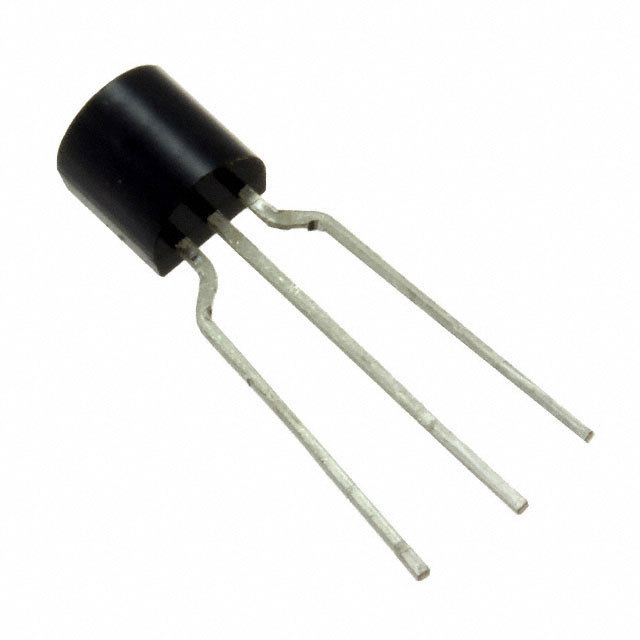
LMT85LP
TO-92 (AKA (2): LP)
3
4.30 mm × 3.50 mm
Through-hole; straight leads
(2)
LMT85LPG
TO-92S (AKA
3
4.00 mm × 3.15 mm
Through-hole; straight leads
LMT85LPM
TO-92 (AKA (2): LPM)
3
4.30 mm × 3.50 mm
Through-hole; formed leads
LMT85DCK-Q1
SOT (AKA (2): SC70, DCK)
5
2.00 mm × 1.25 mm
Surface Mount
(1)
(2)
: LPG)
For all available packages and complete order numbers, see the Package Option addendum at the end of the data sheet.
AKA = Also Known As
Table 2. Comparable Alternative Devices
DEVICE NAME
AVERAGE OUTPUT SENSOR GAIN
POWER SUPPLY RANGE
LMT84
–5.5 mV/°C
1.5 V to 5.5 V
LMT85
–8.2 mV/°C
1.8 V to 5.5 V
LMT86
–10.9 mV/°C
2.2 V to 5.5 V
LMT87
–13.6 mV/°C
2.7 V to 5.5 V
Copyright © 2013–2017, Texas Instruments Incorporated
3
�LMT85
ZHCSCG0E – MARCH 2013 – REVISED OCTOBER 2017
www.ti.com.cn
6 Pin Configuration and Functions
LP Package
3-Pin TO-92
(Top View)
DCK Package
5-Pin SOT/SC70
(Top View)
1
5
GND
VDD
2
LMT85
GND
3
4
OUT
VDD
1
D
VD
G
3 D
N
2 T
U
O
LPG Package
3-Pin TO-92S
(Top View)
Scale: 4:1
1
2
3
LPM Package
3-Pin TO-92
(Top View)
1 T
U
O
3
D
VD
2 D
N
G
Scale: 4:1
1
D
VD
2 T
U
O
3 D
N
G
Scale: 4:1
Pin Functions
PIN
NAME
GND
SOT (SC70)
TO-92
TO-92S
2 (1) , 5
3
2
TYPE
Ground
DESCRIPTION
EQUIVALENT CIRCUIT
N/A
FUNCTION
Power Supply Ground
VDD
OUT
3
2
1
Analog
Output
Outputs a voltage that is inversely
proportional to temperature
GND
VDD
(1)
4
1, 4
1
3
Power
N/A
Positive Supply Voltage
Direct connection to the back side of the die
Copyright © 2013–2017, Texas Instruments Incorporated
�LMT85
www.ti.com.cn
ZHCSCG0E – MARCH 2013 – REVISED OCTOBER 2017
7 Specifications
7.1 Absolute Maximum Ratings
See
(1) (2)
MIN
MAX
UNIT
Supply voltage
−0.3
6
V
Voltage at output pin
−0.3
(VDD + 0.5)
V
–7
7
mA
–5
5
mA
150
°C
150
°C
Output current
Input current at any pin
(3)
Maximum junction temperature (TJMAX)
Storage temperature, Tstg
(1)
(2)
(3)
–65
Stresses beyond those listed under Absolute Maximum Ratings may cause permanent damage to the device. These are stress ratings
only, which do not imply functional operation of the device at these or any other conditions beyond those indicated under Recommended
Operating Conditions. Exposure to absolute-maximum-rated conditions for extended periods may affect device reliability
Soldering process must comply with Reflow Temperature Profile specifications. Refer towww.ti.com/packaging .
When the input voltage (VI) at any pin exceeds power supplies (VI < GND or VI > V), the current at that pin should be limited to 5 mA.
7.2 ESD Ratings
VALUE
UNIT
LMT85LP in TO-92/TO-92S package
V(ESD)
Electrostatic
discharge
Human-body model (HBM), per ANSI/ESDA/JEDEC JS-001 (1) (2)
±2500
Charged-device model (CDM), per JEDEC specification JESD22-C101 (3)
±1000
Human-body model (HBM), per JESD22-A114 (2)
±2500
Charged-device model (CDM), per JEDEC specification JESD22-C101 (3)
±1000
V
LMT85DCK in SC70 package
V(ESD)
(1)
(2)
(3)
Electrostatic
discharge
V
JEDEC document JEP155 states that 500-V HBM allows safe manufacturing with a standard ESD control process.
The human body model is a 100-pF capacitor discharged through a 1.5-kΩ resistor into each pin.
JEDEC document JEP157 states that 250-V CDM allows safe manufacturing with a standard ESD control process.
7.3 Recommended Operating Conditions
MIN
Specified temperature
MAX
UNIT
TMIN ≤ TA ≤ TMAX
°C
−50 ≤ TA ≤ 150
°C
Supply voltage (VDD)
1.8
5.5
V
7.4 Thermal Information (1)
THERMAL METRIC (2)
(3) (4)
LMT85/
LMT85-Q1
LMT85LP
LMT85LPG
DCK (SOT/SC70)
LP/LPM (TO-92)
LPG (TO-92S)
5 PINS
3 PINS
3 PINS
275
167
UNIT
RθJA
Junction-to-ambient thermal resistance
130.4
°C/W
RθJC(top)
Junction-to-case (top) thermal resistance
84
90
64.2
°C/W
RθJB
Junction-to-board thermal resistance
56
146
106.2
°C/W
ψJT
Junction-to-top characterization parameter
1.2
35
14.6
°C/W
ψJB
Junction-to-board characterization parameter
55
146
106.2
°C/W
(1)
(2)
(3)
(4)
For information on self-heating and thermal response time, see section Mounting and Thermal Conductivity.
For more information about traditional and new thermal metrics, see the IC Package Thermal Metrics application report.
The junction to ambient thermal resistance (RθJA) under natural convection is obtained in a simulation on a JEDEC-standard, High-K
board as specified in JESD51-7, in an environment described in JESD51-2. Exposed pad packages assume that thermal vias are
included in the PCB, per JESD 51-5.
Changes in output due to self-heating can be computed by multiplying the internal dissipation by the thermal resistance.
Copyright © 2013–2017, Texas Instruments Incorporated
5
�LMT85
ZHCSCG0E – MARCH 2013 – REVISED OCTOBER 2017
www.ti.com.cn
7.5 Accuracy Characteristics
These limits do not include DC load regulation. These stated accuracy limits are with reference to the values in Table 3.
MIN (1)
TYP (2)
MAX (1)
TA = TJ= 20°C to 150°C; VDD = 1.8 V to 5.5 V
–2.7
±0.4
2.7
°C
TA = TJ= 0°C to 150°C; VDD = 1.9 V to 5.5 V
–2.7
±0.7
2.7
°C
PARAMETER
(3)
Temperature accuracy
TEST CONDITIONS
TA = TJ= 0°C to 150°C; VDD = 2.6 V to 5.5 V
±0.3
TA = TJ= –50°C to 0°C; VDD = 2.3 V to 5.5 V
–2.7
(1)
(2)
(3)
°C
±0.7
TA = TJ= –50°C to 0°C; VDD = 2.9 V to 5.5 V
UNIT
2.7
±0.25
°C
°C
Limits are specific to TI's AOQL (Average Outgoing Quality Level).
Typicals are at TJ = TA = 25°C and represent most likely parametric norm.
Accuracy is defined as the error between the measured and reference output voltages, tabulated in the Transfer Table at the specified
conditions of supply gain setting, voltage, and temperature (expressed in °C). Accuracy limits include line regulation within the specified
conditions. Accuracy limits do not include load regulation; they assume no DC load.
7.6 Electrical Characteristics
Unless otherwise noted, these specifications apply for VDD = +1.8V to +5.5V. MIN and MAX limits apply for TA = TJ = TMIN to
TMAX, unless otherwise noted; typical values apply for TA = TJ = 25°C.
PARAMETER
Average sensor gain (output
transfer function slope)
Load regulation
Line regulation
IS
CL
6
(1)
–30°C and 90°C used to calculate average sensor gain
Source ≤ 50 μA, (VDD - VOUT) ≥ 200 mV
–1
(2)
MAX
(1)
UNIT
mV/°C
–0.22
0.26
(4)
(5)
TYP
–8.2
mV
1
200
mV
μV/V
TA = TJ = 30°C to 150°C, (VDD - VOUT) ≥ 100 mV
5.4
8.1
μA
TA = TJ = -50°C to 150°C, (VDD - VOUT) ≥ 100 mV
5.4
9
μA
1.9
ms
+50
µA
Output load capacitance
Output drive
(5)
MIN
Sink ≤ 50 μA, VOUT ≥ 200 mV
Supply current
Power-on time
(1)
(2)
(3)
(4)
(3)
TEST CONDITIONS
1100
CL= 0 pF to 1100 pF
TA = TJ = 25°C
0.7
–50
pF
Limits are specific to TI's AOQL (Average Outgoing Quality Level).
Typicals are at TJ = TA = 25°C and represent most likely parametric norm.
Source currents are flowing out of the LMT85. Sink currents are flowing into the LMT85.
Line regulation (DC) is calculated by subtracting the output voltage at the highest supply voltage from the output voltage at the lowest
supply voltage. The typical DC line regulation specification does not include the output voltage shift discussed in Output Voltage Shift.
Specified by design and characterization.
Copyright © 2013–2017, Texas Instruments Incorporated
�LMT85
www.ti.com.cn
ZHCSCG0E – MARCH 2013 – REVISED OCTOBER 2017
7.7 Typical Characteristics
4
Minimum Operating Temperature (ƒC)
40
TEMPERATURE ERROR (ºC)
3
2
1
0
-1
-2
-3
-4
-50
-25
0
25
50
75
100 125 150
30
20
10
0
±10
±20
±30
±40
±50
1.50 2.00 2.50 3.00 3.50 4.00 4.50 5.00 5.50
Supply Voltage (V)
TEMPERATURE (ºC)
C002
Figure 1. Temperature Error vs Temperature
Figure 2. Minimum Operating Temperature vs
Supply Voltage
Figure 3. Supply Current vs Temperature
Figure 4. Supply Current vs Supply Voltage
Figure 5. Load Regulation, Sourcing Current
Figure 6. Load Regulation, Sinking Current
Copyright © 2013–2017, Texas Instruments Incorporated
7
�LMT85
ZHCSCG0E – MARCH 2013 – REVISED OCTOBER 2017
www.ti.com.cn
Typical Characteristics (continued)
Figure 7. Change in Vout vs Overhead Voltage
Figure 8. Supply-Noise Gain vs Frequency
100%
FINAL TEMPERATURE
90%
80%
70%
60%
50%
40%
30%
20%
LMT8xLPG
Thermistor
10%
0
0
Figure 9. Output Voltage vs Supply Voltage
20
40
60
TIME (s)
80
100
D003
Figure 10. LMT85LPG Thermal Response vs Common
Leaded Thermistor With 1.2-m/s Airflow
8
Copyright © 2013–2017, Texas Instruments Incorporated
�LMT85
www.ti.com.cn
ZHCSCG0E – MARCH 2013 – REVISED OCTOBER 2017
8 Detailed Description
8.1 Overview
The LMT85 is an analog output temperature sensor. The temperature sensing element is comprised of a simple
base emitter junction that is forward biased by a current source. The temperature-sensing element is then
buffered by an amplifier and provided to the OUT pin. The amplifier has a simple push-pull output stage thus
providing a low impedance output source.
8.2 Functional Block Diagram
Full-Range Celsius Temperature Sensor (−50°C to 150°C).
VDD
OUT
Thermal Diodes
GND
8.3 Feature Description
8.3.1 LMT85 Transfer Function
The output voltage of the LMT85, across the complete operating temperature range, is shown in Table 3. This
table is the reference from which the LMT85 accuracy specifications (listed in the Accuracy Characteristics
section) are determined. This table can be used, for example, in a host processor look-up table. A file containing
this data is available for download at the LMT85 product folder under Tools and Software Models.
Table 3. LMT85 Transfer Table
TEMP
(°C)
VOUT
(mV)
TEMP
(°C)
VOUT
(mV)
TEMP
(°C)
VOUT
(mV)
TEMP
(°C)
VOUT
(mV)
TEMP
(°C)
VOUT
(mV)
-50
1955
-10
1648
30
1324
70
991
110
651
-49
1949
-9
1639
31
1316
71
983
111
642
-48
1942
-8
1631
32
1308
72
974
112
634
-47
1935
-7
1623
33
1299
73
966
113
625
-46
1928
-6
1615
34
1291
74
957
114
617
-45
1921
-5
1607
35
1283
75
949
115
608
-44
1915
-4
1599
36
1275
76
941
116
599
-43
1908
-3
1591
37
1267
77
932
117
591
-42
1900
-2
1583
38
1258
78
924
118
582
-41
1892
-1
1575
39
1250
79
915
119
573
-40
1885
0
1567
40
1242
80
907
120
565
-39
1877
1
1559
41
1234
81
898
121
556
-38
1869
2
1551
42
1225
82
890
122
547
Copyright © 2013–2017, Texas Instruments Incorporated
9
�LMT85
ZHCSCG0E – MARCH 2013 – REVISED OCTOBER 2017
www.ti.com.cn
Feature Description (continued)
Table 3. LMT85 Transfer Table (continued)
TEMP
(°C)
VOUT
(mV)
TEMP
(°C)
VOUT
(mV)
TEMP
(°C)
VOUT
(mV)
TEMP
(°C)
VOUT
(mV)
TEMP
(°C)
VOUT
(mV)
-37
1861
3
1543
43
1217
83
881
123
539
-36
1853
4
1535
44
1209
84
873
124
530
-35
1845
5
1527
45
1201
85
865
125
521
-34
1838
6
1519
46
1192
86
856
126
513
-33
1830
7
1511
47
1184
87
848
127
504
-32
1822
8
1502
48
1176
88
839
128
495
-31
1814
9
1494
49
1167
89
831
129
487
-30
1806
10
1486
50
1159
90
822
130
478
-29
1798
11
1478
51
1151
91
814
131
469
-28
1790
12
1470
52
1143
92
805
132
460
-27
1783
13
1462
53
1134
93
797
133
452
-26
1775
14
1454
54
1126
94
788
134
443
-25
1767
15
1446
55
1118
95
779
135
434
-24
1759
16
1438
56
1109
96
771
136
425
-23
1751
17
1430
57
1101
97
762
137
416
-22
1743
18
1421
58
1093
98
754
138
408
-21
1735
19
1413
59
1084
99
745
139
399
-20
1727
20
1405
60
1076
100
737
140
390
-19
1719
21
1397
61
1067
101
728
141
381
-18
1711
22
1389
62
1059
102
720
142
372
-17
1703
23
1381
63
1051
103
711
143
363
-16
1695
24
1373
64
1042
104
702
144
354
-15
1687
25
1365
65
1034
105
694
145
346
-14
1679
26
1356
66
1025
106
685
146
337
-13
1671
27
1348
67
1017
107
677
147
328
-12
1663
28
1340
68
1008
108
668
148
319
-11
1656
29
1332
69
1000
109
660
149
310
150
301
Although the LMT85 is very linear, its response does have a slight umbrella parabolic shape. This shape is very
accurately reflected in Table 3. The Transfer Table can be calculated by using the parabolic equation
(Equation 1).
mV
mV
ª
º ª
2º
VTEMP mV = 1324.0mV - «8.194
T - 30°C » - «0.00262 2 T - 30°C »
°C
¬
¼ ¬
°C
¼
(1)
The parabolic equation is an approximation of the transfer table and the accuracy of the equation degrades
slightly at the temperature range extremes. Equation 1 can be solved for T resulting in:
T
8 . 194
8 . 194
2
4 u 0 . 00262 u 1324
2 u 0 . 00262
VTEMP mV
30
(2)
For an even less accurate linear transfer function approximation, a line can easily be calculated over the desired
temperature range using values from the Table and a two-point equation (Equation 3):
·
¹
V - V1 =
V2 - V1
T2 - T1
· u (T - T1)
¹
where
•
•
•
•
10
V is in mV,
T is in °C,
T1 and V1 are the coordinates of the lowest temperature,
and T2 and V2 are the coordinates of the highest temperature.
(3)
Copyright © 2013–2017, Texas Instruments Incorporated
�LMT85
www.ti.com.cn
ZHCSCG0E – MARCH 2013 – REVISED OCTOBER 2017
For example, if the user wanted to resolve this equation, over a temperature range of 20°C to 50°C, they would
proceed as follows:
1159 mV - 1405 mV·
u (T - 20oC)
50oC - 20oC
¹
·
¹
V - 1405 mV =
(4)
o
o
V - 1405 mV = (-8.20 mV / C) u (T - 20 C)
(5)
o
V = (-8.20 mV / C) u T + 1569 mV
(6)
Using this method of linear approximation, the transfer function can be approximated for one or more
temperature ranges of interest.
8.4 Device Functional Modes
8.4.1 Mounting and Thermal Conductivity
The LMT85 can be applied easily in the same way as other integrated-circuit temperature sensors. It can be
glued or cemented to a surface.
To ensure good thermal conductivity, the backside of the LMT85 die is directly attached to the GND pin. The
temperatures of the lands and traces to the other leads of the LMT85 will also affect the temperature reading.
Alternatively, the LMT85 can be mounted inside a sealed-end metal tube, and can then be dipped into a bath or
screwed into a threaded hole in a tank. As with any IC, the LMT85 and accompanying wiring and circuits must be
kept insulated and dry, to avoid leakage and corrosion. This is especially true if the circuit may operate at cold
temperatures where condensation can occur. If moisture creates a short circuit from the output to ground or VDD,
the output from the LMT85 will not be correct. Printed-circuit coatings are often used to ensure that moisture
cannot corrode the leads or circuit traces.
The thermal resistance junction to ambient (RθJA or θJA) is the parameter used to calculate the rise of a device
junction temperature due to its power dissipation. Use Equation 7 to calculate the rise in the LMT85 die
temperature:
TJ = TA + TJA ª¬(VDDIS ) + (VDD - VOUT ) IL º¼
where
•
•
•
•
TA is the ambient temperature,
IS is the supply current,
ILis the load current on the output,
and VO is the output voltage.
(7)
For example, in an application where TA = 30°C, VDD = 5 V, IS = 5.4 μA, VOUT = 1324 mV, and IL = 2 μA, the
junction temperature would be 30.014°C, showing a self-heating error of only 0.014°C. Because the junction
temperature of the LMT85 is the actual temperature being measured, take care to minimize the load current that
the LMT85 is required to drive. Thermal Information shows the thermal resistance of the LMT85.
8.4.2 Output and Noise Considerations
A push-pull output gives the LMT85 the ability to sink and source significant current. This is beneficial when, for
example, driving dynamic loads like an input stage on an analog-to-digital converter (ADC). In these applications
the source current is required to quickly charge the input capacitor of the ADC. The LMT85 device is ideal for this
and other applications which require strong source or sink current.
The LMT85 supply-noise gain (the ratio of the AC signal on VOUT to the AC signal on VDD) was measured during
bench tests. The typical attenuation is shown in Figure 8 found in the Typical Characteristics . A load capacitor
on the output can help to filter noise.
For operation in very noisy environments, some bypass capacitance should be present on the supply within
approximately 5 centimeters of the LMT85.
Copyright © 2013–2017, Texas Instruments Incorporated
11
�LMT85
ZHCSCG0E – MARCH 2013 – REVISED OCTOBER 2017
www.ti.com.cn
Device Functional Modes (continued)
8.4.3 Capacitive Loads
The LMT85 handles capacitive loading well. In an extremely noisy environment, or when driving a switched
sampling input on an ADC, it may be necessary to add some filtering to minimize noise coupling. Without any
precautions, the LMT85 can drive a capacitive load less than or equal to 1100 pF as shown in Figure 11. For
capacitive loads greater than 1100 pF, a series resistor may be required on the output, as shown in Figure 12.
VDD
LMT85
OPTIONAL
BYPASS
CAPACITANCE
OUT
GND
CLOAD ” 1100 pF
Figure 11. LMT85 No Decoupling Required for Capacitive Loads Less Than 1100 pF
VDD
RS
LMT85
OPTIONAL
BYPASS
CAPACITANCE
OUT
GND
CLOAD > 1100 pF
Figure 12. LMT85 with Series Resistor for Capacitive Loading Greater Than 1100 pF
Table 4. Recommended Series Resistor Values
CLOAD
MINIMUM RS
1.1 nF to 99 nF
3 kΩ
100 nF to 999 nF
1.5 kΩ
1 μF
800 Ω
8.4.4 Output Voltage Shift
The LMT85 is very linear over temperature and supply voltage range. Due to the intrinsic behavior of an
NMOS/PMOS rail-to-rail buffer, a slight shift in the output can occur when the supply voltage is ramped over the
operating range of the device. The location of the shift is determined by the relative levels of VDD and VOUT. The
shift typically occurs when VDD- VOUT = 1 V.
This slight shift (a few millivolts) takes place over a wide change (approximately 200 mV) in VDD or VOUT.
Because the shift takes place over a wide temperature change of 5°C to 20°C, VOUT is always monotonic. The
accuracy specifications in the Accuracy Characteristics table already include this possible shift.
12
Copyright © 2013–2017, Texas Instruments Incorporated
�LMT85
www.ti.com.cn
ZHCSCG0E – MARCH 2013 – REVISED OCTOBER 2017
9 Application and Implementation
NOTE
Information in the following applications sections is not part of the TI component
specification, and TI does not warrant its accuracy or completeness. TI’s customers are
responsible for determining suitability of components for their purposes. Customers should
validate and test their design implementation to confirm system functionality.
9.1 Application Information
The LMT85 features make it suitable for many general temperature-sensing applications. It can operate down to
1.8-V supply with 5.4-µA power consumption, making it ideal for battery powered devices. Package options like
the through-hole TO-92 package allow the LMT85 to be mounted onboard, off-board, to a heat sink, or on
multiple unique locations in the same application.
9.2 Typical Applications
9.2.1 Connection to an ADC
Simplified Input Circuit of
SAR Analog-to-Digital Converter
Reset
+1.8V to +5.5V
Input
Pin
LMT85
VDD
CBP
RMUX
RSS
Sample
OUT
GND
CFILTER
CMUX
CSAMPLE
Figure 13. Suggested Connection to a Sampling Analog-to-Digital Converter Input Stage
9.2.1.1 Design Requirements
Most CMOS ADCs found in microcontrollers and ASICs have a sampled data comparator input structure. When
the ADC charges the sampling cap, it requires instantaneous charge from the output of the analog source such
as the LMT85 temperature sensor and many op amps. This requirement is easily accommodated by the addition
of a capacitor (CFILTER).
9.2.1.2 Detailed Design Procedure
The size of CFILTER depends on the size of the sampling capacitor and the sampling frequency. Because not all
ADCs have identical input stages, the charge requirements will vary. This general ADC application is shown as
an example only.
9.2.1.3 Application Curve
Figure 14. Analog Output Transfer Function
Copyright © 2013–2017, Texas Instruments Incorporated
13
�LMT85
ZHCSCG0E – MARCH 2013 – REVISED OCTOBER 2017
www.ti.com.cn
Typical Applications (continued)
9.2.2 Conserving Power Dissipation With Shutdown
VDD
SHUTDOWN
VOUT
LMT85
Any logic
device output
Figure 15. Simple Shutdown Connection of the LMT85
9.2.2.1 Design Requirements
Because the power consumption of the LMT85 is less than 9 µA, it can simply be powered directly from any logic
gate output and therefore not require a specific shutdown pin. The device can even be powered directly from a
micro controller GPIO. In this way, it can easily be turned off for cases such as battery-powered systems where
power savings are critical.
9.2.2.2 Detailed Design Procedure
Simply connect the VDD pin of the LMT85 directly to the logic shutdown signal from a microcontroller.
9.2.2.3 Application Curves
Time: 500 µs/div; Top Trace: VDD 1 V/div;
Bottom Trace: OUT 1 V/div
Figure 16. Output Turnon Response Time Without a
Capacitive Load and VDD = 3.3 V
Time: 500 µs/div; Top trace: VDD 2 V/div;
Bottom trace: OUT 1 V/div
Figure 17. Output Turnon Response Time Without a
Capacitive Load and VDD = 5 V
Time: 500 µs/div; Top trace: VDD 1V/div;
Bottom trace: OUT 1 V/div
Figure 18. Output Turnon Response Time With 1.1-nF
Capacitive Load and VDD = 3.3 V
Time: 500 µs/div; Top trace: VDD 2 V/div;
Bottom trace: OUT 1 V/div
Figure 19. Output Turnon Response Time With 1.1-nF
Capacitive Load and VDD = 5 V
10 Power Supply Recommendations
The low supply current and supply range (1.8 V to 5.5 V) of the LMT85 allow the device to easily be powered
from many sources. Power supply bypassing is optional and is mainly dependent on the noise on the power
supply used. In noisy systems it may be necessary to add bypass capacitors to lower the noise that is coupled to
the output of the LMT85.
14
Copyright © 2013–2017, Texas Instruments Incorporated
�LMT85
www.ti.com.cn
ZHCSCG0E – MARCH 2013 – REVISED OCTOBER 2017
11 Layout
11.1 Layout Guidelines
The LMT85 is extremely simple to layout. If a power-supply bypass capacitor is used, it should be connected as
shown in the Layout Example
11.2 Layout Example
VIA to ground plane
VIA to power plane
VDD
GND
GND
0.01µ F
OUT
VDD
Figure 20. SC70 Package Recommended Layout
GND
OUT
VDD
Figure 21. TO-92 LP Package Recommended Layout
GND
OUT
VDD
Figure 22. TO-92 LPM Package Recommended Layout
版权 © 2013–2017, Texas Instruments Incorporated
15
�LMT85
ZHCSCG0E – MARCH 2013 – REVISED OCTOBER 2017
www.ti.com.cn
12 器件和文档支持
12.1 接收文档更新通知
要接收文档更新通知,请导航至 TI.com 上的器件产品文件夹。单击右上角的通知我 进行注册,即可每周接收产品
信息更改摘要。有关更改的详细信息,请查看任何已修订文档中包含的修订历史记录。
12.2 社区资源
下列链接提供到 TI 社区资源的连接。链接的内容由各个分销商“按照原样”提供。这些内容并不构成 TI 技术规范,
并且不一定反映 TI 的观点;请参阅 TI 的 《使用条款》。
TI E2E™ 在线社区 TI 的工程师对工程师 (E2E) 社区。此社区的创建目的在于促进工程师之间的协作。在
e2e.ti.com 中,您可以咨询问题、分享知识、拓展思路并与同行工程师一道帮助解决问题。
设计支持
TI 参考设计支持 可帮助您快速查找有帮助的 E2E 论坛、设计支持工具以及技术支持的联系信息。
12.3 商标
E2E is a trademark of Texas Instruments.
All other trademarks are the property of their respective owners.
12.4 静电放电警告
这些装置包含有限的内置 ESD 保护。 存储或装卸时,应将导线一起截短或将装置放置于导电泡棉中,以防止 MOS 门极遭受静电损
伤。
12.5 Glossary
SLYZ022 — TI Glossary.
This glossary lists and explains terms, acronyms, and definitions.
13 机械、封装和可订购信息
以下页面包含机械、封装和可订购信息。这些信息是指定器件的最新可用数据。这些数据如有变更,恕不另行通知
和修订此文档。如欲获取此数据表的浏览器版本,请参阅左侧的导航。
16
版权 © 2013–2017, Texas Instruments Incorporated
�PACKAGE OPTION ADDENDUM
www.ti.com
10-Dec-2020
PACKAGING INFORMATION
Orderable Device
Status
(1)
Package Type Package Pins Package
Drawing
Qty
Eco Plan
(2)
Lead finish/
Ball material
MSL Peak Temp
Op Temp (°C)
Device Marking
(3)
(4/5)
(6)
LMT85DCKR
ACTIVE
SC70
DCK
5
3000
RoHS & Green
SN
Level-1-260C-UNLIM
-50 to 150
BPA
LMT85DCKT
ACTIVE
SC70
DCK
5
250
RoHS & Green
SN
Level-1-260C-UNLIM
-50 to 150
BPA
LMT85LP
ACTIVE
TO-92
LP
3
1800
RoHS & Green
SN
N / A for Pkg Type
-50 to 150
LMT85
LMT85LPG
ACTIVE
TO-92
LPG
3
1000
RoHS & Green
SN
N / A for Pkg Type
-50 to 150
LMT85
LMT85LPGM
ACTIVE
TO-92
LPG
3
3000
RoHS & Green
SN
N / A for Pkg Type
-50 to 150
LMT85
LMT85LPM
ACTIVE
TO-92
LP
3
2000
RoHS & Green
SN
N / A for Pkg Type
-50 to 150
LMT85
(1)
The marketing status values are defined as follows:
ACTIVE: Product device recommended for new designs.
LIFEBUY: TI has announced that the device will be discontinued, and a lifetime-buy period is in effect.
NRND: Not recommended for new designs. Device is in production to support existing customers, but TI does not recommend using this part in a new design.
PREVIEW: Device has been announced but is not in production. Samples may or may not be available.
OBSOLETE: TI has discontinued the production of the device.
(2)
RoHS: TI defines "RoHS" to mean semiconductor products that are compliant with the current EU RoHS requirements for all 10 RoHS substances, including the requirement that RoHS substance
do not exceed 0.1% by weight in homogeneous materials. Where designed to be soldered at high temperatures, "RoHS" products are suitable for use in specified lead-free processes. TI may
reference these types of products as "Pb-Free".
RoHS Exempt: TI defines "RoHS Exempt" to mean products that contain lead but are compliant with EU RoHS pursuant to a specific EU RoHS exemption.
Green: TI defines "Green" to mean the content of Chlorine (Cl) and Bromine (Br) based flame retardants meet JS709B low halogen requirements of