User's Guide
SNWA009A – March 2008 – Revised April 2013
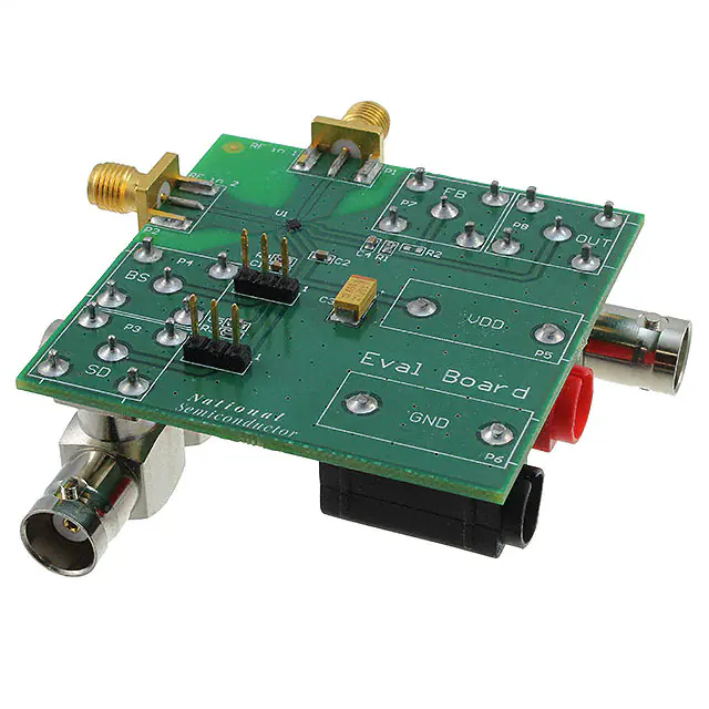
AN-1806 LMV232 Evaluation Board
1
General Description
This board, the LMV232TLEVAL, can be used to evaluate the Texas Instruments LMV232 dual-channel
mean square power detector. The LMV232 mean square power detector is particularly suited for accurate
power measurement of RF modulated signals that exhibit large peak to average ratios, that is, large
variations of the signal envelope. Such noise-like signals are encountered in applications such as CDMA
and wideband CDMA cellphones.
2
Basic Operation
The LMV232 power detector provides an accurate power measurement for arbitrary input signals, low and
high peak-to-average ratios and crest factors. This is because its operation is not based on peak
detection, but on direct determination of the mean square value. The single supply, ranging from 2.5V to
3.3V, can be applied through connectors P5 and P6 of the evaluation board. The device has two digital
interfaces. The signal connected to P3 (SD) puts the device in an active mode or a shutdown mode. When
SD = HIGH, the device is in shutdown, if SD = LOW the device is active. The signal connected to P4 (BS)
selects the active RF input signal. When BS = HIGH, RFIN1 is active (P1). When BS = LOW, RFIN2 is
active (P2). The output voltage is measured through connector P8. Connector P7 can be used to monitor
the voltage on the FB pin of the LMV232 when a 0Ω resistor is placed in R2. Further details can be found
in the Application Notes section of LMV232 Dual-Channel Integrated Mean Square Power Detector for
CDMA & WCDMA (SNWS017).
The LMV232 conversion gain and bandwidth can be configured by a resistor and a capacitor. Resistor R1
sets the conversion gain from RFIN to the output voltage. A higher resistor value will result in a higher
conversion gain. The maximum dynamic range is achieved when the resistor value is as high as possible,
i.e. the output signal just doesn’t clip and the voltage stays within the baseband ADC input range. The
filter bandwidth is adjusted by capacitor C4. The capacitor value should be chosen such that the response
time of the device is fast enough and modulation on the RF input signal is not visible at the output (ripple
suppression). The -3 dB filter bandwidth of the output filter is determined by the time constant R1*C4.
Generally a capacitor value of 1.5 nF is a good choice.
All trademarks are the property of their respective owners.
SNWA009A – March 2008 – Revised April 2013
Submit Documentation Feedback
Copyright © 2008–2013, Texas Instruments Incorporated
AN-1806 LMV232 Evaluation Board
1
�Schematics
3
www.ti.com
Schematics
The schematic of the evaluation board is shown in Figure 1.
VDD
R2
N/C
U1
P1
B3
RFIN1
RFIN1
RFIN2
P2
RFIN2
A1
A2
A3
C3
SD
VDD
C2
R1
6.2 k:
C4
1.5 nF
OUT
P8
OUT
B1
BS
GND
P3
J1
SD
R3
100 k:
C5
10 nF
P5
VDD
VDD
P4
FB
FB
LMV232
C1
P7
P6
+ C3
100 µF
GND
J2
U1 ± pin B3
C2
10 nF
U1 ± pin B1
BS
R4
100 k:
C1
10 nF
Figure 1. Schematic of the Evaluation Board
4
Bill of Materials
The bill of material (BOM) of the evaluation board is listed in Table 1.
Table 1. Bill of Materials of the Evaluation Board
2
Designator
Description
Comment
C1, C2, C5
0603 Capacitor
10 nF
C3
Case_C Capacitor
100 µF
C4
0603 Capacitor
1.5 nF
J1, J2
Header 1 × 3
For Jumper
P1, P2
Connector
SMA
P3, P4, P7, P8
Connector
BNC
P5, P6
Connector
Banana
R1
0603 Resistor
6.2 kΩ
R2
0603 Resistor
Not Connected
R3, R4
0603 Resistor
100 kΩ
U1
DSBGA
LMV232
AN-1806 LMV232 Evaluation Board
SNWA009A – March 2008 – Revised April 2013
Submit Documentation Feedback
Copyright © 2008–2013, Texas Instruments Incorporated
�Layout
www.ti.com
5
Layout
The layout of the evaluation board is shown in Figure 2.
All Layers
Silk Screen
Figure 2. Layout of the Evaluation Board
SNWA009A – March 2008 – Revised April 2013
Submit Documentation Feedback
Copyright © 2008–2013, Texas Instruments Incorporated
AN-1806 LMV232 Evaluation Board
3
�Measurement Procedure
6
www.ti.com
Measurement Procedure
The performance of the LMV232 can be measured with the setup given in Figure 3.
In this measurement example a supply voltage of 2.7V is applied by the power supply. The LMV232 is set
in active mode by connecting SD (P3) to GND, while RFIN1 is selected by connecting BS (P4) to 2.7V. Both
RFIN2 (P2) and FB (P7) can be left unconnected. The resulting DC output voltage is measured with a
multimeter connected to OUT (P8).
VDD
Power
Supply
VDD
BS
P4
RFIN1
RF Signal
Generator
RFIN2
P5
Evaluation Board
LMV232
P1
OUT
P8
Digital
Volt
Meter
FB
P7
P2
P3
SD
P6
GND
Figure 3. Measurement Setup
7
Measurement Results
Figure 4 and Figure 5 show the measurement results for the LMV232. The power is swept at 900 MHz for
different temperatures (Figure 4). The resulting error with respect to an ideal fitted curve is shown in
Figure 5.
Figure 4. VOUT - VPEDESTAL vs. RF Input Power
at 900 MHz
4
AN-1806 LMV232 Evaluation Board
Figure 5. Input Referred Error vs. RF Input Power
at 900 MHz
SNWA009A – March 2008 – Revised April 2013
Submit Documentation Feedback
Copyright © 2008–2013, Texas Instruments Incorporated
�IMPORTANT NOTICE
Texas Instruments Incorporated and its subsidiaries (TI) reserve the right to make corrections, enhancements, improvements and other
changes to its semiconductor products and services per JESD46, latest issue, and to discontinue any product or service per JESD48, latest
issue. Buyers should obtain the latest relevant information before placing orders and should verify that such information is current and
complete. All semiconductor products (also referred to herein as “components”) are sold subject to TI’s terms and conditions of sale
supplied at the time of order acknowledgment.
TI warrants performance of its components to the specifications applicable at the time of sale, in accordance with the warranty in TI’s terms
and conditions of sale of semiconductor products. Testing and other quality control techniques are used to the extent TI deems necessary
to support this warranty. Except where mandated by applicable law, testing of all parameters of each component is not necessarily
performed.
TI assumes no liability for applications assistance or the design of Buyers’ products. Buyers are responsible for their products and
applications using TI components. To minimize the risks associated with Buyers’ products and applications, Buyers should provide
adequate design and operating safeguards.
TI does not warrant or represent that any license, either express or implied, is granted under any patent right, copyright, mask work right, or
other intellectual property right relating to any combination, machine, or process in which TI components or services are used. Information
published by TI regarding third-party products or services does not constitute a license to use such products or services or a warranty or
endorsement thereof. Use of such information may require a license from a third party under the patents or other intellectual property of the
third party, or a license from TI under the patents or other intellectual property of TI.
Reproduction of significant portions of TI information in TI data books or data sheets is permissible only if reproduction is without alteration
and is accompanied by all associated warranties, conditions, limitations, and notices. TI is not responsible or liable for such altered
documentation. Information of third parties may be subject to additional restrictions.
Resale of TI components or services with statements different from or beyond the parameters stated by TI for that component or service
voids all express and any implied warranties for the associated TI component or service and is an unfair and deceptive business practice.
TI is not responsible or liable for any such statements.
Buyer acknowledges and agrees that it is solely responsible for compliance with all legal, regulatory and safety-related requirements
concerning its products, and any use of TI components in its applications, notwithstanding any applications-related information or support
that may be provided by TI. Buyer represents and agrees that it has all the necessary expertise to create and implement safeguards which
anticipate dangerous consequences of failures, monitor failures and their consequences, lessen the likelihood of failures that might cause
harm and take appropriate remedial actions. Buyer will fully indemnify TI and its representatives against any damages arising out of the use
of any TI components in safety-critical applications.
In some cases, TI components may be promoted specifically to facilitate safety-related applications. With such components, TI’s goal is to
help enable customers to design and create their own end-product solutions that meet applicable functional safety standards and
requirements. Nonetheless, such components are subject to these terms.
No TI components are authorized for use in FDA Class III (or similar life-critical medical equipment) unless authorized officers of the parties
have executed a special agreement specifically governing such use.
Only those TI components which TI has specifically designated as military grade or “enhanced plastic” are designed and intended for use in
military/aerospace applications or environments. Buyer acknowledges and agrees that any military or aerospace use of TI components
which have not been so designated is solely at the Buyer's risk, and that Buyer is solely responsible for compliance with all legal and
regulatory requirements in connection with such use.
TI has specifically designated certain components as meeting ISO/TS16949 requirements, mainly for automotive use. In any case of use of
non-designated products, TI will not be responsible for any failure to meet ISO/TS16949.
Products
Applications
Audio
www.ti.com/audio
Automotive and Transportation
www.ti.com/automotive
Amplifiers
amplifier.ti.com
Communications and Telecom
www.ti.com/communications
Data Converters
dataconverter.ti.com
Computers and Peripherals
www.ti.com/computers
DLP® Products
www.dlp.com
Consumer Electronics
www.ti.com/consumer-apps
DSP
dsp.ti.com
Energy and Lighting
www.ti.com/energy
Clocks and Timers
www.ti.com/clocks
Industrial
www.ti.com/industrial
Interface
interface.ti.com
Medical
www.ti.com/medical
Logic
logic.ti.com
Security
www.ti.com/security
Power Mgmt
power.ti.com
Space, Avionics and Defense
www.ti.com/space-avionics-defense
Microcontrollers
microcontroller.ti.com
Video and Imaging
www.ti.com/video
RFID
www.ti-rfid.com
OMAP Applications Processors
www.ti.com/omap
TI E2E Community
e2e.ti.com
Wireless Connectivity
www.ti.com/wirelessconnectivity
Mailing Address: Texas Instruments, Post Office Box 655303, Dallas, Texas 75265
Copyright © 2013, Texas Instruments Incorporated
�