Sample &
Buy
Product
Folder
Support &
Community
Tools &
Software
Technical
Documents
LMV712-N, LMV712-N-Q1
SNOS534J – FEBRUARY 2001 – REVISED NOVEMBER 2016
LMV712-N, LMV712-N-Q1 Low Power, Low Noise, High Output, RRIO Dual Operational
Amplifier With Independent Shutdown
1 Features
3 Description
•
The LMV712-N devices are high-performance
BiCMOS operational amplifiers intended for
applications requiring rail-to-rail inputs combined with
speed and low noise. They offer a bandwidth of
5 MHz and a slew rate of 5 V/µs, and can handle
capacitive loads of up to 200 pF without oscillation.
1
•
•
•
•
•
•
•
•
•
•
•
•
Available In Automotive AEC-Q100 Grade 1
Version (LMV712-N Only)
5-MHz GBP
Slew Rate: 5 V/µs
Low Noise: 20 nV/√Hz
Supply Current: 1.22 mA/Channel
VOS< 3 mV Maximum
Ensured 2.7-V and 5-V Specifications
Temperature Range: –40°C to 125°C
Rail-to-Rail Inputs and Outputs
Unity Gain Stable
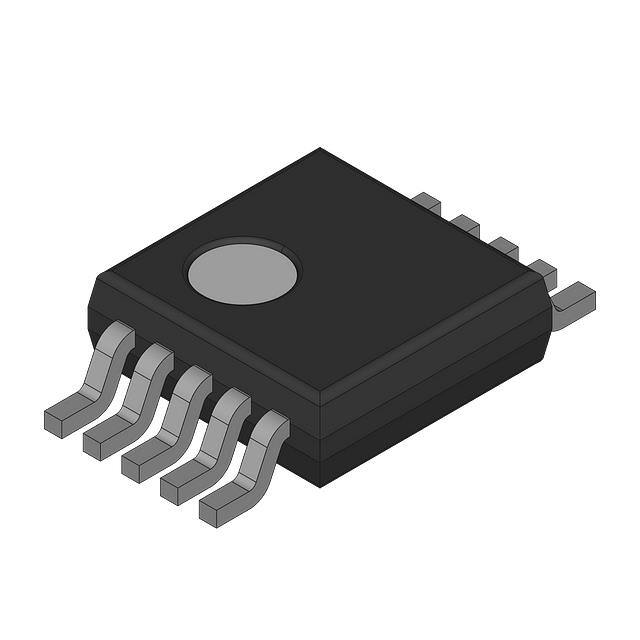
Small Package: 10-Pin DSBGA, 10-Pin WSON,
and 10-Pin VSSOP
1.5-µA Shutdown ICC
2.2-µs Turnon
The LMV712-N is ensured to operate from 2.7 V to
5.5 V and offers two independent shutdown pins. This
feature allows disabling of each device separately
and reduces the supply current to less than 1 µA
typical. The output voltage rapidly ramps up smoothly
with no glitch as the amplifier comes out of the
shutdown mode.
The LMV712-N with the shutdown feature is offered
in space-saving 10-pin DSBGA and 10-pin WSON
packages. It is also offered in 10-pin VSSOP
package. These packages are designed to meet the
demands of small size, low power, and low cost
required by cellular phones and similar batteryoperated portable electronics.
2 Applications
•
•
•
•
•
•
Power Amplifier Control Loops
Cellular Phones
Portable Equipment
Wireless LAN
Radio Systems
Cordless Phones
Device Information(1)
PART NUMBER
LMV712-N
LMV712-N,
LMV712-N-Q1
PACKAGE
BODY SIZE (NOM)
DSBGA (10)
1.75 mm × 2.25 mm
WSON (10)
3.00 mm × 3.00 mm
VSSOP (10)
3.00 mm × 3.00 mm
(1) For all available packages, see the orderable addendum at
the end of the data sheet.
Power Amplifier Control Loop
GSM
ANTENNA
U1
U2
GSM PA
C2
RF Signal
IN
Input
Output
Directional Coupler
OUT
C3
Coupled
VPC
Load
R5
VCC
R2
R1
VCC
C4
BIAS
Schottky Diode
Detector
R3
V+
SD
V-
±
OUT
+
U3
RLOAD
C5
R4
Shut Down
Ramp
Up/Down
Copyright © 2016, Texas Instruments Incorporated
1
An IMPORTANT NOTICE at the end of this data sheet addresses availability, warranty, changes, use in safety-critical applications,
intellectual property matters and other important disclaimers. PRODUCTION DATA.
�LMV712-N, LMV712-N-Q1
SNOS534J – FEBRUARY 2001 – REVISED NOVEMBER 2016
www.ti.com
Table of Contents
1
2
3
4
5
6
Features ..................................................................
Applications ...........................................................
Description .............................................................
Revision History.....................................................
Pin Configuration and Functions .........................
Specifications.........................................................
6.1
6.2
6.3
6.4
6.5
6.6
6.7
7
1
1
1
2
3
6
Absolute Maximum Ratings ...................................... 6
ESD Ratings.............................................................. 6
Recommended Operating Conditions....................... 6
Thermal Information .................................................. 6
Electrical Characteristics – 2.7 V .............................. 7
Electrical Characteristics – 5 V ................................. 9
Typical Characteristics ............................................ 11
Detailed Description ............................................ 16
7.1 Overview ................................................................. 16
7.2 Functional Block Diagram ....................................... 16
7.3 Feature Description ................................................ 16
7.4 Device Functional Modes ....................................... 17
8
Application and Implementation ........................ 19
8.1 Application Information............................................ 19
8.2 Typical Applications ................................................ 19
9 Power Supply Recommendations...................... 22
10 Layout................................................................... 22
10.1 Layout Guidelines ................................................. 22
10.2 Layout Example .................................................... 22
11 Device and Documentation Support ................. 23
11.1
11.2
11.3
11.4
11.5
11.6
Related Links ........................................................
Receiving Notification of Documentation Updates
Community Resources..........................................
Trademarks ...........................................................
Electrostatic Discharge Caution ............................
Glossary ................................................................
23
23
23
23
23
23
12 Mechanical, Packaging, and Orderable
Information ........................................................... 23
4 Revision History
NOTE: Page numbers for previous revisions may differ from page numbers in the current version.
Changes from Revision I (January 2014) to Revision J
Page
•
Added ESD Ratings table, Feature Description section, Device Functional Modes, Application and Implementation
section, Power Supply Recommendations section, Layout section, Device and Documentation Support section, and
Mechanical, Packaging, and Orderable Information section .................................................................................................. 1
•
Deleted Soldering specification from Absolute Maximum Ratings table ................................................................................ 6
•
Changed Thermal Resistance values in Thermal Information table From: 196 To: 84.1 (DSBGA), From: 53.4 To: 70
(WSON), and From: 235 To: 176.8 (VSSOP) ........................................................................................................................ 6
Changes from Revision H (February 2013) to Revision I
•
Page
Added -Q1 part ....................................................................................................................................................................... 1
Changes from Revision G (February 2013) to Revision H
•
2
Page
Changed layout of National Semiconductor Data Sheet to TI format .................................................................................... 1
Submit Documentation Feedback
Copyright © 2001–2016, Texas Instruments Incorporated
Product Folder Links: LMV712-N LMV712-N-Q1
�LMV712-N, LMV712-N-Q1
www.ti.com
SNOS534J – FEBRUARY 2001 – REVISED NOVEMBER 2016
5 Pin Configuration and Functions
YPA Package
10-Pin DSBGA
Top View
A2
+
V
A1
OUTA
A3
OUTB
B1
-INA
B3
-INB
C1
+INA
C3
+INB
D1
SDA
D3
SDB
V
-
D2
Pin Functions: DSBGA Package
PIN
TYPE (1)
DESCRIPTION
NO.
NAME
A1
OUTA
O
Channel A output
A2
V+
P
Positive supply input
A3
OUTB
O
Channel B output
B1
–INA
I
Channel A inverting input
B3
–INB
I
Channel B inverting input
C1
+INA
I
Channel A noninverting input
C3
+INB
I
Channel A noninverting input
D1
SDA
I
Channel A shutdown
D2
V–
P
Negative supply input
D3
SDB
I
Channel B shutdown
(1)
I = Input, O = Output, P = Power
Copyright © 2001–2016, Texas Instruments Incorporated
Product Folder Links: LMV712-N LMV712-N-Q1
Submit Documentation Feedback
3
�LMV712-N, LMV712-N-Q1
SNOS534J – FEBRUARY 2001 – REVISED NOVEMBER 2016
www.ti.com
NGY Package
10-Pin WSON
Top View
OUT A
1
-IN A
2
V+
10
-
9
OUT B
8
-IN B
+
+
-
+IN A
3
V-
4
7
+IN B
SD A
5
6
SD B
-
Pin Functions: WSON Package
PIN
TYPE (1)
DESCRIPTION
NO.
NAME
1
OUT A
O
Channel A output
2
–IN A
I
Channel A inverting input
3
+IN A
I
Channel A noninverting input
4
V–
P
Positive supply input
5
SD A
I
Channel A shutdown
6
SD B
I
Channel B shutdown
7
+IN B
I
Channel B noninverting input
8
–IN A
I
Channel B inverting input
9
OUT B
O
Channel B output
10
V+
P
Positive supply input
11
Thermal Pad
G
Connect thermal pad to V– or leave floating
(1)
4
G = Ground, I = Input, O = Output, P = Power
Submit Documentation Feedback
Copyright © 2001–2016, Texas Instruments Incorporated
Product Folder Links: LMV712-N LMV712-N-Q1
�LMV712-N, LMV712-N-Q1
www.ti.com
SNOS534J – FEBRUARY 2001 – REVISED NOVEMBER 2016
DGS Package
10-Pin VSSOP
Top View
OUT A
-IN A
1
10
2
9
-
+IN A
OUT B
+
3
+
-
8 -IN B
V- 4
7
5
6
SD A
V+
+IN B
SD B
Pin Functions: VSSOP Package
PIN
TYPE (1)
DESCRIPTION
NO.
NAME
1
OUT A
O
Channel A output
2
–IN A
I
Channel A inverting input
3
+IN A
I
Channel A noninverting input
4
V–
P
Negative supply input
5
SD A
I
Channel A shutdown
6
SD B
I
Channel B shutdown
7
+IN B
I
Channel B noninverting input
8
–IN A
I
Channel B inverting input
9
OUT B
O
Channel B output
10
V+
P
Positive supply input
(1)
I = Input, O = Output, P = Power
Copyright © 2001–2016, Texas Instruments Incorporated
Product Folder Links: LMV712-N LMV712-N-Q1
Submit Documentation Feedback
5
�LMV712-N, LMV712-N-Q1
SNOS534J – FEBRUARY 2001 – REVISED NOVEMBER 2016
www.ti.com
6 Specifications
6.1 Absolute Maximum Ratings
over operating free-air temperature range (unless otherwise noted) (1) (2)
MIN
Differential input voltage
(V+) + 0.4
Voltage at input or output pin
+
MAX
–
Supply voltage (V – V )
V+, V–
UNIT
±Supply voltage
(V–) – 0.4
V
6
V
Output short circuit
See (3)
Current at input pin
±10
mA
Current at output pin
±50
mA
TJMAX
Junction temperature (4)
150
°C
Tstg
Storage temperature
150
°C
(1)
(2)
(3)
(4)
–65
Absolute Maximum Ratings indicate limits beyond which damage to the device may occur. Operating Ratings indicate conditions for
which the device is intended to be functional, but specific performance is not ensured. For ensured specifications and the test
conditions, see the Electrical Characteristics.
If Military/Aerospace specified devices are required, please contact the Texas Instruments Sales Office / Distributors for availability and
specifications.
Shorting circuit output to either V+ or V− adversely affects reliability.
The maximum power dissipation is a function of TJ(MAX) and RθJA. The maximum allowable power dissipation at any ambient
temperature is PD = (TJ(MAX) – TA) / RθJA. All numbers apply for packages soldered directly onto a PCB.
6.2 ESD Ratings
VALUE
V(ESD)
(1)
(2)
Electrostatic discharge
Human-body model (HBM), per ANSI/ESDA/JEDEC JS-001 (1)
±1500
Charged-device model (CDM), per JEDEC specification JESD22-C101 (2)
±150
UNIT
V
JEDEC document JEP155 states that 500-V HBM allows safe manufacturing with a standard ESD control process.
JEDEC document JEP157 states that 250-V CDM allows safe manufacturing with a standard ESD control process.
6.3 Recommended Operating Conditions
over operating free-air temperature range (unless otherwise noted)
Supply voltage
Operating temperature
MIN
MAX
2.7
5.5
UNIT
V
LMV712
–40
85
°C
LMV712-Q1
–40
125
°C
6.4 Thermal Information
LMV712-N, LMV712-N-Q1
THERMAL METRIC (1)
YPA (DSBGA)
NGY (WSON)
DGS (VSSOP)
10 PINS
10 PINS
10 PINS
UNIT
RθJA
Junction-to-ambient thermal resistance
84.1
70
176.8
°C/W
RθJC(top)
Junction-to-case (top) thermal resistance
0.6
74.7
67.5
°C/W
RθJB
Junction-to-board thermal resistance
21.4
43.7
97.2
°C/W
ψJT
Junction-to-top characterization parameter
2.2
2
9.4
°C/W
ψJB
Junction-to-board characterization parameter
21.3
43.7
95.8
°C/W
RθJC(bot)
Junction-to-case (bottom) thermal resistance
—
11.8
—
°C/W
(1)
6
For more information about traditional and new thermal metrics, see the Semiconductor and IC Package Thermal Metrics application
report.
Submit Documentation Feedback
Copyright © 2001–2016, Texas Instruments Incorporated
Product Folder Links: LMV712-N LMV712-N-Q1
�LMV712-N, LMV712-N-Q1
www.ti.com
SNOS534J – FEBRUARY 2001 – REVISED NOVEMBER 2016
6.5 Electrical Characteristics – 2.7 V
All limits ensured for V+ = 2.7 V, V − = 0 V, VCM = 1.35 V, TA = 25°C, and RL > 1 mΩ (unless otherwise noted)
PARAMETER
TEST CONDITIONS
Input offset voltage
(WSON and VSSOP)
VCM = 0.85 V and
VCM = 1.85 V
Input offset voltage
(DSBGA only)
VCM = 0.85 V and
VCM = 1.85 V
VOS
LMV712-Q1
Common mode rejection
ratio
0 V ≤ VCM ≤ 2.7 V
2.7 V ≤ V+ ≤ 5 V,
VCM = 0.85 V
PSRR
Power supply rejection ratio
+
2.7 V ≤ V ≤ 5 V,
VCM = 1.85 V
CMVR
Common mode voltage
For CMRR ≥ 50 dB
Sourcing
VO = 0 V
ISC
Output short circuit current
Sinking
VO = 2.7 V
RL = 10 kΩ to
1.35 V
Output swing
MAX (1)
0.4
3
−40°C ≤ TJ ≤ 85°C (LMV712) or
−40°C ≤ TJ ≤ 125°C (LMV712-Q1)
TA = 25°C
3
−40°C ≤ TJ ≤ 85°C (LMV712) or
−40°C ≤ TJ ≤ 125°C (LMV712-Q1)
5.5
130
50
−40°C ≤ TJ ≤ 85°C (LMV712) or
−40°C ≤ TJ ≤ 125°C (LMV712-Q1)
45
TA = 25°C
70
−40°C ≤ TJ ≤ 85°C (LMV712) or
−40°C ≤ TJ ≤ 125°C (LMV712-Q1)
68
TA = 25°C
70
−40°C ≤ TJ ≤ 85°C (LMV712) or
−40°C ≤ TJ ≤ 125°C (LMV712-Q1)
68
−0.2
V+
75
dB
90
15
−40°C ≤ TJ ≤ 85°C (LMV712) or
−40°C ≤ TJ ≤ 125°C (LMV712-Q1)
12
TA = 25°C
25
−40°C ≤ TJ ≤ 85°C (LMV712) or
−40°C ≤ TJ ≤ 125°C (LMV712-Q1)
22
2.62
−0.3
TA = 25°C
2.68
2.6
2.52
TA = 25°C
On mode
IS
Supply current per channel
2.5
(1)
(2)
−40°C ≤ TJ ≤ 85°C (LMV712) or
−40°C ≤ TJ ≤ 125°C (LMV712-Q1)
0.23
0.3
10
200
1.22
1.7
−40°C ≤ TJ ≤ 85°C (LMV712) or
−40°C ≤ TJ ≤ 125°C (LMV712-Q1)
TA = 25°C
Shutdown mode
V
2.55
0.05
Output voltage in shutdown
0.12
0.15
−40°C ≤ TJ ≤ 85°C (LMV712) or
−40°C ≤ TJ ≤ 125°C (LMV712-Q1)
VO(SD)
V
mA
50
0.01
−40°C ≤ TJ ≤ 85°C (LMV712) or
−40°C ≤ TJ ≤ 125°C (LMV712-Q1)
2.9
25
−40°C ≤ TJ ≤ 85°C (LMV712) or
−40°C ≤ TJ ≤ 125°C (LMV712-Q1)
RL = 600 Ω to
1.35 V
dB
90
3
TA = 25°C
TA = 25°C
pA
3740
TA = 25°C
−40°C ≤ TJ ≤ 85°C (LMV712) or
−40°C ≤ TJ ≤ 125°C (LMV712-Q1)
mV
115
5.5
−40°C ≤ TJ ≤ 125°C
TA = 25°C
7
9
TA = 25°C
V-
UNIT
3.2
TA = 25°C
VO
TYP (2)
−40°C ≤ TJ ≤ 85°C
Input bias current
CMRR
TA = 25°C
TA = 25°C
LMV712
IB
MIN (1)
1.9
0.12
mV
mA
1.5
2
µA
All limits are ensured by testing or statistical analysis.
Typical values represent the most likely parametric norm as determined at the time of characterization. Actual typical values may vary
over time and also depend on the application and configuration. The typical values are not tested and are not ensured on shipped
production material.
Copyright © 2001–2016, Texas Instruments Incorporated
Product Folder Links: LMV712-N LMV712-N-Q1
Submit Documentation Feedback
7
�LMV712-N, LMV712-N-Q1
SNOS534J – FEBRUARY 2001 – REVISED NOVEMBER 2016
www.ti.com
Electrical Characteristics – 2.7 V (continued)
All limits ensured for V+ = 2.7 V, V − = 0 V, VCM = 1.35 V, TA = 25°C, and RL > 1 mΩ (unless otherwise noted)
PARAMETER
LMV712 Sourcing
RL = 10 kΩ
VO = 1.35 V
to 2.3 V
LMV712-Q1
LMV712 Sinking
RL = 10 kΩ
VO = 0.4 V
to 1.35 V
LMV712-Q1
AVOL
Large signal voltage gain
MIN (1)
TYP (2)
TA = 25°C
80
115
−40°C ≤ TJ ≤ 85°C
76
TEST CONDITIONS
LMV712 Sourcing
RL = 600 Ω
VO = 1.35 V
to 2.2 V
LMV712-Q1
LMV712 Sinking
RL = 600 Ω
VO = 0.5 V
to 1.35 V
LMV712-Q1
TA = 25°C
MAX (1)
UNIT
115
−40°C ≤ TJ ≤ 125°C
69
TA = 25°C
80
−40°C ≤ TJ ≤ 85°C
76
TA = 25°C
113
113
−40°C ≤ TJ ≤ 125°C
69
TA = 25°C
80
−40°C ≤ TJ ≤ 85°C
76
TA = 25°C
dB
97
97
−40°C ≤ TJ ≤ 125°C
64
TA = 25°C
80
−40°C ≤ TJ ≤ 85°C
76
TA = 25°C
100
100
−40°C ≤ TJ ≤ 125°C
62
On mode
2.4
2.0
VSD
Shutdown pin voltage
GBWP
Gain-bandwidth product
5
MHz
SR
Slew rate (3)
5
V/µs
φm
Phase margin
60
°
en
Input referred voltage noise
Turnon time from shutdown
TON
DSBGA turnon time from
shutdown
(3)
8
Shutdown mode
1
f = 1 kHz
20
TA = 25°C
2.2
−40°C ≤ TJ ≤ 85°C (LMV712) or
−40°C ≤ TJ ≤ 125°C (LMV712-Q1)
0.8
V
nV/√Hz
4
4.6
TA = 25°C
6
−40°C ≤ TJ ≤ 85°C (LMV712) or
−40°C ≤ TJ ≤ 125°C (LMV712-Q1)
8
µs
Number specified is the slower of the positive and negative slew rates.
Submit Documentation Feedback
Copyright © 2001–2016, Texas Instruments Incorporated
Product Folder Links: LMV712-N LMV712-N-Q1
�LMV712-N, LMV712-N-Q1
www.ti.com
SNOS534J – FEBRUARY 2001 – REVISED NOVEMBER 2016
6.6 Electrical Characteristics – 5 V
All limits ensured for V+ = 5 V, V − = 0 V, VCM = 2.5 V, TA = 25°C, and RL > 1 mΩ (unless otherwise noted)
PARAMETER
TEST CONDITIONS
Input offset voltage
(WSON and VSSOP)
VCM = 0.85 V and
VCM = 1.85 V
Input offset voltage
(DSBGA only)
VCM = 0.85 V and
VCM = 1.85 V
VOS
IB
Input bias current
LMV712
LMV712-Q1
CMRR
Common mode rejection
ratio
0 V ≤ VCM ≤ 5 V
2.7 V ≤ V+ ≤ 5 V,
VCM = 0.85 V
PSRR
CMVR
Power supply rejection
ratio
Common mode voltage
2.7 V ≤ V+ ≤ 5 V,
VCM = 1.85 V
For CMRR ≥ 50 dB
Sourcing
VO = 0 V
ISC
Output short circuit current
Sinking
VO = 5 V
TA = 25°C
Output swing
MAX (1)
0.4
3
TA = 25°C
3
−40°C ≤ TJ ≤ 85°C (LMV712) or
−40°C ≤ TJ ≤ 125°C (LMV712-Q1)
5.5
130
−40°C ≤ TJ ≤ 125°C
3600
TA = 25°C
50
−40°C ≤ TJ ≤ 85°C (LMV712) or
−40°C ≤ TJ ≤ 125°C (LMV712-Q1)
45
TA = 25°C
70
−40°C ≤ TJ ≤ 85°C (LMV712) or
−40°C ≤ TJ ≤ 125°C (LMV712-Q1)
68
TA = 25°C
70
−40°C ≤ TJ ≤ 85°C (LMV712) or
−40°C ≤ TJ ≤ 125°C (LMV712-Q1)
68
−0.2
V+
20
−40°C ≤ TJ ≤ 85°C (LMV712) or
−40°C ≤ TJ ≤ 125°C (LMV712-Q1)
18
TA = 25°C
25
−40°C ≤ TJ ≤ 85°C (LMV712) or
−40°C ≤ TJ ≤ 125°C (LMV712-Q1)
21
4.92
dB
90
−40°C ≤ TJ ≤ 85°C (LMV712) or
−40°C ≤ TJ ≤ 125°C (LMV712-Q1)
TA = 25°C
−0.3
TA = 25°C
On mode
IS
Supply current per channel
4.98
4.9
(1)
(2)
−40°C ≤ TJ ≤ 85°C (LMV712) or
−40°C ≤ TJ ≤ 125°C (LMV712-Q1)
0.12
0.15
4.82
V
4.85
4.8
0.23
0.3
10
200
1.17
1.7
−40°C ≤ TJ ≤ 85°C (LMV712) or
−40°C ≤ TJ ≤ 125°C (LMV712-Q1)
TA = 25°C
Shutdown mode
V
mA
50
0.05
Output voltage in shutdown
5.2
35
−40°C ≤ TJ ≤ 85°C (LMV712) or
−40°C ≤ TJ ≤ 125°C (LMV712-Q1)
VO(SD)
dB
90
0.01
TA = 25°C
pA
80
5.3
TA = 25°C
−40°C ≤ TJ ≤ 85°C (LMV712) or
−40°C ≤ TJ ≤ 125°C (LMV712-Q1)
mV
115
−40°C ≤ TJ ≤ 85°C
−40°C ≤ TJ ≤ 85°C (LMV712) or
−40°C ≤ TJ ≤ 125°C (LMV712-Q1)
RL = 600 Ω to 2.5 V
7
9
TA = 25°C
V-
UNIT
3.2
TA = 25°C
VO
TYP (2)
−40°C ≤ TJ ≤ 85°C (LMV712) or
−40°C ≤ TJ ≤ 125°C (LMV712-Q1)
TA = 25°C
RL = 10 kΩ to 2.5 V
MIN (1)
1.9
0.12
mV
mA
1.5
2
µA
All limits are ensured by testing or statistical analysis.
Typical values represent the most likely parametric norm as determined at the time of characterization. Actual typical values may vary
over time and also depend on the application and configuration. The typical values are not tested and are not ensured on shipped
production material.
Copyright © 2001–2016, Texas Instruments Incorporated
Product Folder Links: LMV712-N LMV712-N-Q1
Submit Documentation Feedback
9
�LMV712-N, LMV712-N-Q1
SNOS534J – FEBRUARY 2001 – REVISED NOVEMBER 2016
www.ti.com
Electrical Characteristics – 5 V (continued)
All limits ensured for V+ = 5 V, V − = 0 V, VCM = 2.5 V, TA = 25°C, and RL > 1 mΩ (unless otherwise noted)
PARAMETER
LMV712 Sourcing
RL = 10 kΩ
VO = 2.5 V to 4.6 V
LMV712-Q1
LMV712 Sinking
RL = 10 kΩ
VO = 0.4 V to 2.5 V
LMV712-Q1
AVOL
Large signal voltage gain
MIN (1)
TYP (2)
TA = 25°C
80
130
−40°C ≤ TJ ≤ 85°C
76
TEST CONDITIONS
LMV712 Sourcing
RL = 600 Ω
VO = 2.5 V to 4.6 V
LMV712-Q1
LMV712 Sinking
RL = 600 Ω
VO = 0.4 V to 2.5 V
LMV712-Q1
TA = 25°C
MAX (1)
UNIT
130
−40°C ≤ TJ ≤ 125°C
69
TA = 25°C
80
−40°C ≤ TJ ≤ 85°C
76
TA = 25°C
130
130
−40°C ≤ TJ ≤ 125°C
69
TA = 25°C
80
−40°C ≤ TJ ≤ 85°C
76
TA = 25°C
dB
110
110
−40°C ≤ TJ ≤ 125°C
69
TA = 25°C
80
−40°C ≤ TJ ≤ 85°C
76
TA = 25°C
107
107
−40°C ≤ TJ ≤ 125°C
69
On mode
4.5
3.5
VSD
Shutdown pin voltage
GBWP
Gain-bandwidth product
5
MHz
SR
Slew rate (3)
5
V/µs
φm
Phase margin
60
°
en
Input referred voltage
noise
f = 1 kHz
20
nV/√Hz
TA = 25°C
1.6
Turnon time for shutdown
TON
DSBGA turnon time for
shutdown
(3)
10
Shutdown mode
1.5
−40°C ≤ TJ ≤ 85°C (LMV712) or
−40°C ≤ TJ ≤ 125°C (LMV712-Q1)
0.8
V
4
4.6
TA = 25°C
6
−40°C ≤ TJ ≤ 85°C (LMV712) or
−40°C ≤ TJ ≤ 125°C (LMV712-Q1)
8
µs
Number specified is the slower of the positive and negative slew rates.
Submit Documentation Feedback
Copyright © 2001–2016, Texas Instruments Incorporated
Product Folder Links: LMV712-N LMV712-N-Q1
�LMV712-N, LMV712-N-Q1
www.ti.com
SNOS534J – FEBRUARY 2001 – REVISED NOVEMBER 2016
6.7 Typical Characteristics
TA = 25°C, VS = 5 V, and single supply (unless otherwise noted)
1.5
0.6
85°C
1.3
0.5
25°C
IS (µA)
IS (mA)
1.1
-40°C
0.4
0.9
0.3
0.7
0.5
2.7 3.0
3.5
4.0
4.5
0.2
2.7 3.0
5.0
3.5
4.0
4.5
5.0
SUPPLY VOLTAGE (V)
SUPPLY VOLTAGE (V)
Figure 1. Supply Current Per Channel vs Supply Voltage
Figure 2. Supply Current vs Supply Voltage (Shutdown)
0
100
+85°C
-200
+70°C
10
-40°C
-600
IBIAS (pA)
VOS (µV)
-400
25°C
+50°C
1
+25°C
-800
0°C
0.1
85°C
-25°C
-1000
-40°C
0.01
-1200
0
1
2
3
4
5
0
2
3
4
5
VCM (V)
Figure 3. VOS vs VCM
Figure 4. IB vs VCM Over Temperature
100
160
90
140
VOUT FROM GND (mV)
25°C
85°C
120
+
VOUT FROM V (mV)
1
VCM (V)
100
80
-40°C
25°C
85°C
80
70
60
-40°C
50
60
40
2.7
3.0
3.5
4.0
4.5
5.0
40
2.7
3.0
3.5
4.0
4.5
5.0
VS (V)
VS (V)
RL = 600 Ω
RL = 600 Ω
Figure 5. Output Positive Swing vs Supply Voltage
Figure 6. Output Negative Swing vs Supply Voltage
Copyright © 2001–2016, Texas Instruments Incorporated
Product Folder Links: LMV712-N LMV712-N-Q1
Submit Documentation Feedback
11
�LMV712-N, LMV712-N-Q1
SNOS534J – FEBRUARY 2001 – REVISED NOVEMBER 2016
www.ti.com
Typical Characteristics (continued)
TA = 25°C, VS = 5 V, and single supply (unless otherwise noted)
35
30
85°C
85°C
30
25
25
ISOURCE (mA)
ISOURCE (mA)
25°C
20
-40°C
15
10
-40°C
25°C
20
15
10
5
5
0
-0.3
0
0.2
0.7
1.2
1.7
2.2
0
2.7
1
2
+
3
4
VS = 5 V
VS = 2.7 V
Figure 7. Sourcing Current vs Output Voltage
Figure 8. Sourcing Current vs Output Voltage
90
70
85°C
85°C
80
60
70
50
25°C
60
25°C
40
ISINK (mA)
ISINK (mA)
5
VOUT (V)
VOUT FROM V (V)
30
-40°C
20
-40°C
50
40
30
20
10
10
0
0
-10
-0.3
-10
0.2
0.7
1.7
1.2
VOUT (V)
2.2
0
2.7
1
2
3
4
5
VOUT (V)
VS = 2.7 V
VS = 5V
Figure 9. Sinking Current vs Output Voltage
Figure 10. Sinking Current vs Output Voltage
100
100
90
90
80
80
NEGATIVE
NEGATIVE
70
PSRR (dB)
PSRR (dB)
70
60
50
40
POSITIVE
30
60
50
40
POSITIVE
30
20
20
10
10
0
0
10
100
1k
10k
100k
1M
10
VS = 2.7 V
Submit Documentation Feedback
1k
10k
100k
1M
VS = 5 V
Figure 11. PSRR vs Frequency
12
100
FREQUENCY (Hz)
FREQUENCY (Hz)
Figure 12. PSRR vs Frequency
Copyright © 2001–2016, Texas Instruments Incorporated
Product Folder Links: LMV712-N LMV712-N-Q1
�LMV712-N, LMV712-N-Q1
www.ti.com
SNOS534J – FEBRUARY 2001 – REVISED NOVEMBER 2016
Typical Characteristics (continued)
TA = 25°C, VS = 5 V, and single supply (unless otherwise noted)
100
100
VS = 2.7V
90
90
dVCM = 0.2V TO 1.2V
80
80
70
CMRR (dB)
60
50
40
50
40
30
30
20
20
10
10
0
0
10
100
1k
10k
100
10k
100k
1M
Figure 13. CMRR vs Frequency
Figure 14. CMRR vs Frequency
80
VS = 2.7V
VS = 5V
70
60
60
10k:
50
RL = 10k:
90
20
60
40
RL = 600:
RL = 600:
30
90
60
20
10
30
10
30
0
0
0
0
10k:
-20
1k
10k
100k
RL = 10k:
-10
1M
-20
1k
10M
10k
FREQUENCY (Hz)
70
100k
1M
10M
FREQUENCY (Hz)
Figure 15. Open Loop Frequency Response vs RL
80
Figure 16. Open Loop Frequency Response vs RL
80
VS = 2.7V
VS = 5V
70
CL = 0pF
CL = 0pF
60
90
50
60
50
60
30
CL = 100pF
30
20
0
CL = 1000pF
CL = 100pF
30
30
0
CL = 1000pF
20
CL = 1000pF
0
0
CL = 100pF
-10
-20
1k
40
10
CL = 1000pF
10
GAIN (dB)
90
PHASE (Deg)
60
40
PHASE (Deg)
600:
GAIN (dB)
600:
30
PHASE (Deg)
50
-10
GAIN (dB)
1k
FREQUENCY (Hz)
80
40
dVCM = 2V TO 3V
10
1M
100k
VS = 5V
FREQUENCY (Hz)
70
GAIN (dB)
60
PHASE (Deg)
CMRR (dB)
70
10k
100k
CL = 100pF
-10
CL = 0pF
1M
10M
-20
1k
CL = 0pF
10k
100k
1M
10M
FREQUENCY (Hz)
FREQUENCY (Hz)
Figure 17. Open Loop Frequency Response vs CL
Figure 18. Open Loop Frequency Response vs CL
Copyright © 2001–2016, Texas Instruments Incorporated
Product Folder Links: LMV712-N LMV712-N-Q1
Submit Documentation Feedback
13
�LMV712-N, LMV712-N-Q1
SNOS534J – FEBRUARY 2001 – REVISED NOVEMBER 2016
www.ti.com
Typical Characteristics (continued)
TA = 25°C, VS = 5 V, and single supply (unless otherwise noted)
1000
1000
VS = 5V
INPUT VOLTAGE NOISE (nV/ Hz)
INPUT VOLTAGE NOISE (nV/ Hz)
VS = 2.7V
VCM = 1.35V
VSD = 2.7V
100
10
VCM = 2.5V
VSD = 5V
100
10
1
1
1
10
100
1k
FREQUENCY (Hz)
10k
1
100k
10k
100k
OUTPUT
OUTPUT
(1V/div)
(1V/div)
INPUT
INPUT
100
1k
FREQUENCY (Hz)
Figure 20. Voltage Noise vs Frequency
Figure 19. Voltage Noise vs Frequency
TIME (500ns/div)
TIME (500ns/div)
VS = 2.7 V
VS = 5 V
Figure 22. Non-Inverting Large Signal Pulse Response
OUTPUT
OUTPUT
(50mV/div)
(50mV/div)
INPUT
INPUT
Figure 21. Non-Inverting Large Signal Pulse Response
TIME (500ns/div)
TIME (500ns/div)
VS = 2.7 V
VS = 5 V
Figure 23. Non-Inverting Small Signal Pulse Response
14
10
Submit Documentation Feedback
Figure 24. Non-Inverting Small Signal Pulse Response
Copyright © 2001–2016, Texas Instruments Incorporated
Product Folder Links: LMV712-N LMV712-N-Q1
�LMV712-N, LMV712-N-Q1
www.ti.com
SNOS534J – FEBRUARY 2001 – REVISED NOVEMBER 2016
Typical Characteristics (continued)
INPUT
OUTPUT
OUTPUT
(1V/div)
(1V/div)
INPUT
TA = 25°C, VS = 5 V, and single supply (unless otherwise noted)
TIME (500ns/div)
TIME (500ns/div)
VS = 2.7 V
VS = 5 V
Figure 26. Inverting Large Signal Pulse Response
(50mV/div)
OUTPUT
OUTPUT
(50mV/div)
INPUT
INPUT
Figure 25. Inverting Large Signal Pulse Response
TIME (500ns/div)
TIME (500ns/div)
VS = 2.7 V
VS = 5 V
Figure 27. Inverting Small Signal Pulse Response
OUTPUT
VOLTAGE
30
SHUTDOWN
PULSE
26
CCM TO GROUND
FMEAS = 1MHz
FOLLOWER CONFIG
24
VOUT FOLLOWS VIN (VCM)
28
TIME (2µs/div)
CDIFF (pF)
(2V/div)
Figure 28. Inverting Small Signal Pulse Response
22
20
18
16
14
12
10
0
1
2
3
4
5
VCM (V)
VS = 5 V
VS = 5 V
Figure 29. Turnon Time Response
Figure 30. Input Common Mode Capacitance vs VCM
Copyright © 2001–2016, Texas Instruments Incorporated
Product Folder Links: LMV712-N LMV712-N-Q1
Submit Documentation Feedback
15
�LMV712-N, LMV712-N-Q1
SNOS534J – FEBRUARY 2001 – REVISED NOVEMBER 2016
www.ti.com
7 Detailed Description
7.1 Overview
The LMV712-N features low voltage, low power, and rail-to-rail output operational amplifiers designed for lowvoltage portable applications.
7.2 Functional Block Diagram
V+
VBIAS
IP
MP3
Q2
MP1
MP2
MP4
Q1
MN2
IN-
IN+
CLASS AB
CONTROL
OUT
MN3
MN1
Q3
Q4
Q5
IN
Q6
MN4
VBIAS
V-
BIAS
CONTROL
SD
Copyright © 2016, Texas Instruments Incorporated
7.3 Feature Description
Rail-to-rail input is achieved by using in parallel, one NMOS differential pair (MN1 and MN2) and one PMOS
differential pair (MP1 and MP2). When the common mode input voltage (VCM) is near V+, the NMOS pair is on
and the PMOS pair is off. When VCM is near V−, the NMOS pair is off and the PMOS pair is on. When VCM is
between V+ and V−, internal logic decides how much current each differential pair receives. This special logic
ensures stable and low distortion amplifier operation within the entire common mode voltage range.
Because both input stages have their own offset voltage (VOS) characteristic, the offset voltage of the LMV712-N
becomes a function of VCM. VOS has a crossover point at 1.4 V above V− (see Figure 3). Caution must be taken
in situations where input signal amplitude is comparable to VOS value or the design requires high accuracy. In
these situations, it is necessary for the input signal to avoid the crossover point.
The current coming out of the input differential pairs gets mirrored through two folded cascode stages (Q1, Q2,
Q3, Q4) into the class AB control block. This circuitry generates voltage gain, defines the dominant pole of the op
amp and limits the maximum current flowing at the output stage. MN3 introduces a voltage level shift and acts as
a high impedance to low impedance buffer.
16
Submit Documentation Feedback
Copyright © 2001–2016, Texas Instruments Incorporated
Product Folder Links: LMV712-N LMV712-N-Q1
�LMV712-N, LMV712-N-Q1
www.ti.com
SNOS534J – FEBRUARY 2001 – REVISED NOVEMBER 2016
Feature Description (continued)
The output stage is composed of a PMOS and a NPN transistor in a common source or emitter configuration,
delivering a rail-to-rail output excursion.
The MN4 transistor ensures that the LMV712-N output remains near V− when the amplifier is in shutdown mode.
7.4 Device Functional Modes
7.4.1 Shutdown Pin
The LMV712-N offers independent shutdown pins for the dual amplifiers. When the shutdown pin is tied low, the
respective amplifier shuts down and the supply current is reduced to less than 1 µA. In shutdown mode, the
output level of the amplifier stays at V−. In a 2.7-V operation, when a voltage from 1.5 V to 2.7 V is applied to the
shutdown pin, the amplifier is enabled. As the amplifier is coming out of the shutdown mode, the output
waveform ramps up without any glitch.
OUTPUT
VOLTAGE
(2V/div)
SHUTDOWN
PULSE
TIME (2µs/div)
Figure 31. Output Recovery from Shutdown
A glitch-free output waveform is highly desirable in many applications, one of which is power amplifier control
loops. In this application, the LMV712-N is used to drive the power amplifier's power control. If the LMV712-N did
not have a smooth output ramp during turn on, it would directly cause the power amplifier to produce a glitch at
its output. This adversely affects the performance of the system.
To enable the amplifier, the shutdown pin must be pulled high. It must not be left floating in the event that any
leakage current may inadvertently turn off the amplifier.
7.4.2 Capacitive Load Tolerance
The LMV712-N can directly drive 200 pF in unity-gain without oscillation. The unity-gain follower is the most
sensitive configuration to capacitive loading. Direct capacitive loading reduces the phase margin of amplifiers.
The combination of the amplifier's output impedance and the capacitive load induces phase lag. This results in
either an underdamped pulse response or oscillation. To drive a heavier capacitive load, TI recommends the
circuit in Figure 32.
Copyright © 2001–2016, Texas Instruments Incorporated
Product Folder Links: LMV712-N LMV712-N-Q1
Submit Documentation Feedback
17
�LMV712-N, LMV712-N-Q1
SNOS534J – FEBRUARY 2001 – REVISED NOVEMBER 2016
www.ti.com
Device Functional Modes (continued)
RISO
_
VOUT
+
VIN
CL
Figure 32. Driving Heavy Capacitive Loads
In Figure 32, the isolation resistor RISO and the load capacitor CL form a pole to increase stability by adding more
phase margin to the overall system. The desired performance depends on the value of RISO. The bigger the RISO
resistor value, the more stable VOUT is. But the DC accuracy is degraded when the RISO gets bigger. If there were
a load resistor in the application, the output voltage would be divided by RISO and the load resistor.
Figure 33 is an improvement to the one in Figure 32 because it provides DC accuracy as well as AC stability. In
Figure 33, RF provides the DC accuracy by using feed-forward techniques to connect VIN to RL. CF and RISO
serve to counteract the loss of phase margin by feeding the high frequency component of the output signal back
to the inverting input of the amplifier, thereby preserving phase margin in the overall feedback loop. Increased
capacitive drive is possible by increasing the value of CF. This in turn slows down the pulse response.
RF
CF
_
VIN
RISO
VOUT
+
CL
RL
Figure 33. Enhanced DC Accuracy
7.4.3 Latchup
CMOS devices tend to be susceptible to latchup due to their internal parasitic SCR (silicon controlled rectifier)
effects. The input and output pins look similar to the gate of the SCR. There is a minimum current required to
trigger the SCR gate lead. The LMV712-N is designed to withstand 150-mA surge current on all the pins. Some
resistive method must be used to isolate any capacitance from supplying excess current to the pins. In addition,
like an SCR, there is a minimum holding current for any latchup mode. Limiting current to the supply pins also
inhibits latchup susceptibility.
18
Submit Documentation Feedback
Copyright © 2001–2016, Texas Instruments Incorporated
Product Folder Links: LMV712-N LMV712-N-Q1
�LMV712-N, LMV712-N-Q1
www.ti.com
SNOS534J – FEBRUARY 2001 – REVISED NOVEMBER 2016
8 Application and Implementation
NOTE
Information in the following applications sections is not part of the TI component
specification, and TI does not warrant its accuracy or completeness. TI’s customers are
responsible for determining suitability of components for their purposes. Customers should
validate and test their design implementation to confirm system functionality.
8.1 Application Information
The LMV712-N devices are dual op amps derived from the LMV711 single op amp. Figure 34 contains a
simplified schematic of one channel of the LMV712-N.
8.2 Typical Applications
8.2.1 High-Side Current-Sensing
V
+
+
R1
±
2 kŸ
RSENSE
±
0.2
Q1
2N3906
R2
+
2 kŸ
VOUT
Load
R3
10 kŸ
ICHARGE
VOUT
RSENSE x R3
x ICh arg e 1 : x ICh arg e
R1
Copyright © 2016, Texas Instruments Incorporated
Figure 34. High-Side, Current-Sensing Schematic
8.2.1.1 Design Requirements
The high-side, current-sensing circuit (Figure 34) is commonly used in a battery charger to monitor charging
current to prevent over charging. A sense resistor RSENSE is connected to the battery directly. This system
requires an op amp with rail-to-rail input. The LMV712-N is ideal for this application because its common-mode
input range goes up to the rail.
8.2.1.2 Detailed Design Procedure
As seen in (Figure 34), the ICHARGE current flowing through sense resistor RSENSE develops a voltage drop equal
to VSENSE. The voltage at the negative sense point is now less than the positive sense point by an amount
proportional to the VSENSE voltage.
The low-bias currents of the LMV712-N causes little voltage drop through R2, so the negative input of the
LMV712-N amplifier is at essentially the same potential as the negative sense input.
The LMV712-N detects this voltage error between its inputs and servo the transistor base to conduct more
current through Q1, increasing the voltage drop across R1 until the LMV712-N inverting input matches the
noninverting input. At this point, the voltage drop across R1 now matches VSENSE.
Copyright © 2001–2016, Texas Instruments Incorporated
Product Folder Links: LMV712-N LMV712-N-Q1
Submit Documentation Feedback
19
�LMV712-N, LMV712-N-Q1
SNOS534J – FEBRUARY 2001 – REVISED NOVEMBER 2016
www.ti.com
Typical Applications (continued)
IG, a current proportional to ICHARGE, flows according to Equation 1.
IG = VRSENSE / R1 = ( RSENSE × ICHARGE ) / R1
(1)
IG also flows through the gain resistor R3 developing a voltage drop equal to Equation 2.
V3 = IG × R3 = ( VRSENSE / R1 ) × R3 = ( ( RSENSE × ICHARGE ) / R2 ) × R3
VOUT = (RSENSE × ICHARGE ) × G
(2)
where
•
G = R3 / R1
(3)
The other channel of the LMV712-N may be used to buffer the voltage across R3 to drive the following stages.
8.2.1.3 Application Curve
5
VOUT (V)
VOUT (V)
4
3
2
1
1
2
3
4
5
ILOAD (A)
C003
Figure 35. High-Side Current-Sensing Results
8.2.2 Peak Detector
R4
10 k
R2
V+
10 k
V+
-
R1
VIN
D1
R3
LMV71x
(A1)
+
LMV71x
(A2)
VO
+
1N914A
R5
C1
10 k
10 k
Reset
2N2945
Copyright © 2016, Texas Instruments Incorporated
Figure 36. Peak Detector Schematic
8.2.2.1 Design Requirements
A peak detector outputs a DC voltage equal to the peak value of the applied AC signal. Peak detectors are used
in many applications, such as test equipment, measurement instrumentation, ultrasonic alarm systems, and so
forth. Figure 36 shows the schematic diagram of a peak detector using LMV712-N. This peak detector basically
consists of a clipper, a parallel RC network, and a voltage follower.
20
Submit Documentation Feedback
Copyright © 2001–2016, Texas Instruments Incorporated
Product Folder Links: LMV712-N LMV712-N-Q1
�LMV712-N, LMV712-N-Q1
www.ti.com
SNOS534J – FEBRUARY 2001 – REVISED NOVEMBER 2016
Typical Applications (continued)
8.2.2.2 Detailed Design Procedure
An AC voltage source applied to VIN charges capacitor C1 to the peak of the input. Diode D1 conducts positive
half cycles, charging C1 to the waveform peak. Including D1 inside the feedback loop of the amplifier removes
the voltage drop of D1 and allows an accurate peak detection of VIN on C1. When the input waveform falls below
the DC peak stored on C1, D1 is reverse biased. The low input bias current of A1 and the reverse biasing of D1
limits current leakage from C1. As a result, C1 retains the peak value even as the waveform drops to zero. A2
further isolates the peak value on C1 while completing the peak detector circuit by operating as a voltage
follower and reporting the peak voltage of C1 at its output.
R5 and C1 are properly selected so that the capacitor is charged rapidly to VIN. During the holding period, the
capacitor slowly discharge through C1, through leakage of the capacitor and the reverse-biased diode, or op amp
bias currents. In any cases the discharging time constant is much larger than the charge time constant. And the
capacitor can hold its voltage long enough to minimize the output ripple.
Resistors R2 and R3 limit the current into the inverting input of A1 and the noninverting input of A2 when power
is disconnected from the circuit. The discharging current from C1 during power off may damage the input circuitry
of the op amps.
The peak detector is reset by applying a positive pulse to the reset transistor. The charge on the capacitor is
dumped into ground, and the detector is ready for another cycle.
The maximum input voltage to this detector must be less than (V+ – VD), where VD is the forward voltage drop of
the diode. Otherwise, the input voltage must be scaled down before applying to the circuit.
8.2.3 GSM Power Amplifier Control Loop
GSM
ANTENNA
U1
U2
GSM PA
C2
RF Signal
Input
Output
Directional Coupler
IN OUT
C3
Coupled
VPC
Load
VCC
R2
R1
VCC
R3
C4
R5
BIAS
Schottky Diode
Detector
V+
±
OUT
SD
+
V-
U3
RLOAD
C5
R4
Shut Down
Ramp
Up/Down
Copyright © 2016, Texas Instruments Incorporated
Figure 37. GSM Power Amplifier Control Loop Schematic
8.2.3.1 Design Requirements
The control loop in Figure 37 controls the output power level of a GSM mobile phones. The control loop is used
to avoid intermodulation of base station receivers, to prevent intermodulation with other mobile phones, and to
minimize power consumption depending on the distance between mobile and base station.
Copyright © 2001–2016, Texas Instruments Incorporated
Product Folder Links: LMV712-N LMV712-N-Q1
Submit Documentation Feedback
21
�LMV712-N, LMV712-N-Q1
SNOS534J – FEBRUARY 2001 – REVISED NOVEMBER 2016
www.ti.com
Typical Applications (continued)
8.2.3.2 Detailed Design Procedure
There are four critical sections in the GSM Power Amplifier Control Loop. The class-C RF power amplifier
provides amplification of the RF signal. A directional coupler couples small amount of RF energy from the output
of the RF P. A. to an envelope detector diode. The detector diode senses the signal level and rectifies it to a DC
level to indicate the signal strength at the antenna. An op amp is used as an error amplifier to process the diode
voltage and ramping voltage. This loop control the power amplifier gain through the op amp and forces the
detector diode voltage and ramping voltage to be equal. Power control is accomplished by changing the ramping
voltage.
The LMV712-N is well suited as an error amplifier in this application. The LMV712-N has an extra shutdown pin
to switch the op amp to shutdown mode. In shutdown mode, the LMV712-N consumes very low current.
Therefore, the power amplifier can be turned off to save battery life. The LMV712-N output is tri-stated when in
shutdown.
9 Power Supply Recommendations
For proper operation, the power supplies must be properly decoupled. For decoupling the supply lines, TI
recommends that 10-nF capacitors be placed as close as possible to the power supply pins of the operational
amplifier. For single supply, place a capacitor between V+ and V– supply leads. For dual supplies, place one
capacitor between V+ and ground, and one capacitor between V– and ground.
10 Layout
10.1 Layout Guidelines
To properly bypass the power supply, several locations on a printed circuit board must be considered. A 6.8 µF
or greater tantalum capacitor must be placed at the point where the power supply for the amplifier is introduced
onto the board. Another 0.1-µF ceramic capacitor must be placed as close as possible to the power supply pin of
the amplifier. If the amplifier is operated in a single power supply, only the V+ pin requires bypassing with a 0.1µF capacitor. If the amplifier is operated in a dual power supply, both V+ and V– pins must be bypassed.
It is good practice to use a ground plane on a printed circuit board to provide all components with a low inductive
ground connection.
Surface mount components in 0805 size or smaller are recommended in the LMV712-N application circuits.
Designers can take advantage of the DSBGA, WSON, and VSSOP miniature sizes to condense board layout to
save space and reduce stray capacitance.
10.2 Layout Example
C3
C1
GND
R2
OUTA
VOUT
C4
V+
V+
R4
GND
R1
VIN
V-
ShutDown
-INA
OUTB
+INA
-INB
V-
+INB
VIN
SDA
SDB
ShutDown
C2
VOUT
GND
R3
Copyright © 2016, Texas Instruments Incorporated
Figure 38. Sample Layout of VSSOP
22
Submit Documentation Feedback
Copyright © 2001–2016, Texas Instruments Incorporated
Product Folder Links: LMV712-N LMV712-N-Q1
�LMV712-N, LMV712-N-Q1
www.ti.com
SNOS534J – FEBRUARY 2001 – REVISED NOVEMBER 2016
11 Device and Documentation Support
11.1 Related Links
The table below lists quick access links. Categories include technical documents, support and community
resources, tools and software, and quick access to sample or buy.
Table 1. Related Links
PARTS
PRODUCT FOLDER
SAMPLE & BUY
TECHNICAL
DOCUMENTS
TOOLS &
SOFTWARE
SUPPORT &
COMMUNITY
LMV712-N
Click here
Click here
Click here
Click here
Click here
LMV712-N-Q1
Click here
Click here
Click here
Click here
Click here
11.2 Receiving Notification of Documentation Updates
To receive notification of documentation updates, navigate to the device product folder on ti.com. In the upper
right corner, click on Alert me to register and receive a weekly digest of any product information that has
changed. For change details, review the revision history included in any revised document.
11.3 Community Resources
The following links connect to TI community resources. Linked contents are provided "AS IS" by the respective
contributors. They do not constitute TI specifications and do not necessarily reflect TI's views; see TI's Terms of
Use.
TI E2E™ Online Community TI's Engineer-to-Engineer (E2E) Community. Created to foster collaboration
among engineers. At e2e.ti.com, you can ask questions, share knowledge, explore ideas and help
solve problems with fellow engineers.
Design Support TI's Design Support Quickly find helpful E2E forums along with design support tools and
contact information for technical support.
11.4 Trademarks
E2E is a trademark of Texas Instruments.
All other trademarks are the property of their respective owners.
11.5 Electrostatic Discharge Caution
These devices have limited built-in ESD protection. The leads should be shorted together or the device placed in conductive foam
during storage or handling to prevent electrostatic damage to the MOS gates.
11.6 Glossary
SLYZ022 — TI Glossary.
This glossary lists and explains terms, acronyms, and definitions.
12 Mechanical, Packaging, and Orderable Information
The following pages include mechanical, packaging, and orderable information. This information is the most
current data available for the designated devices. This data is subject to change without notice and revision of
this document. For browser-based versions of this data sheet, refer to the left-hand navigation.
Copyright © 2001–2016, Texas Instruments Incorporated
Product Folder Links: LMV712-N LMV712-N-Q1
Submit Documentation Feedback
23
�PACKAGE OPTION ADDENDUM
www.ti.com
30-Sep-2021
PACKAGING INFORMATION
Orderable Device
Status
(1)
Package Type Package Pins Package
Drawing
Qty
Eco Plan
(2)
Lead finish/
Ball material
MSL Peak Temp
Op Temp (°C)
Device Marking
(3)
(4/5)
(6)
LMV712LD/NOPB
ACTIVE
WSON
NGY
10
1000
RoHS & Green
SN
Level-3-260C-168 HR
-40 to 85
A62
LMV712LDX/NOPB
ACTIVE
WSON
NGY
10
4500
RoHS & Green
SN
Level-3-260C-168 HR
-40 to 85
A62
LMV712MM
NRND
VSSOP
DGS
10
1000
Non-RoHS
& Green
Call TI
Level-1-260C-UNLIM
-40 to 85
A61
LMV712MM/NOPB
ACTIVE
VSSOP
DGS
10
1000
RoHS & Green
SN
Level-1-260C-UNLIM
-40 to 85
A61
LMV712MMX/NOPB
ACTIVE
VSSOP
DGS
10
3500
RoHS & Green
SN
Level-1-260C-UNLIM
-40 to 85
A61
LMV712Q1MM/NOPB
ACTIVE
VSSOP
DGS
10
1000
RoHS & Green
SN
Level-1-260C-UNLIM
-40 to 125
AUA
LMV712Q1MMX/NOPB
ACTIVE
VSSOP
DGS
10
3500
RoHS & Green
SN
Level-1-260C-UNLIM
-40 to 125
AUA
LMV712TL/NOPB
ACTIVE
DSBGA
YPA
10
250
RoHS & Green
SNAGCU
Level-1-260C-UNLIM
-40 to 85
AU2A
LMV712TLX/NOPB
ACTIVE
DSBGA
YPA
10
3000
RoHS & Green
SNAGCU
Level-1-260C-UNLIM
-40 to 85
AU2A
(1)
The marketing status values are defined as follows:
ACTIVE: Product device recommended for new designs.
LIFEBUY: TI has announced that the device will be discontinued, and a lifetime-buy period is in effect.
NRND: Not recommended for new designs. Device is in production to support existing customers, but TI does not recommend using this part in a new design.
PREVIEW: Device has been announced but is not in production. Samples may or may not be available.
OBSOLETE: TI has discontinued the production of the device.
(2)
RoHS: TI defines "RoHS" to mean semiconductor products that are compliant with the current EU RoHS requirements for all 10 RoHS substances, including the requirement that RoHS substance
do not exceed 0.1% by weight in homogeneous materials. Where designed to be soldered at high temperatures, "RoHS" products are suitable for use in specified lead-free processes. TI may
reference these types of products as "Pb-Free".
RoHS Exempt: TI defines "RoHS Exempt" to mean products that contain lead but are compliant with EU RoHS pursuant to a specific EU RoHS exemption.
Green: TI defines "Green" to mean the content of Chlorine (Cl) and Bromine (Br) based flame retardants meet JS709B low halogen requirements of