Application Report
SNOA497B – September 2007 – Revised April 2013
AN-1698 A Specification for EMI Hardened Operational
Amplifiers
.....................................................................................................................................................
ABSTRACT
This application report presents the background, details, and usage of the EMI Rejection Ratio (EMIRR)
parameter.
1
2
3
4
5
6
Contents
Introduction .................................................................................................................. 2
EMI and Op Amps .......................................................................................................... 2
EMIRR Definition ............................................................................................................ 3
EMIRR Measurement ...................................................................................................... 4
4.1
Op Amp Configuration ............................................................................................. 5
4.2
Applying the RF Signal ............................................................................................ 5
4.3
Isolating the Other Pins ........................................................................................... 5
4.4
Test Circuits ........................................................................................................ 5
Measurement Results for the LMV851/LMV852/LMV854 ............................................................. 9
5.1
EMIRR Vs. Frequency ............................................................................................. 9
5.2
EMIRR Vs. Power ................................................................................................ 10
Typical Applications and EMIRR ........................................................................................ 11
6.1
Signal Path Application .......................................................................................... 11
6.2
Cell Phone Call ................................................................................................... 12
List of Figures
................................................................
.........................................
Coupling the RF Signal to the IN+ Pin Circuit Diagram ................................................................
Coupling the RF Signal to the IN− Pin Circuit Diagram ................................................................
Coupling an RF Signal to Either of the Supply Pins Circuit Diagram ................................................
Coupling an RF Signal to the Output Pin Circuit Diagram .............................................................
EMIRR vs. Frequency for IN+, IN−, VDD, VSS, and OUT ................................................................
EMIRR vs. RF Input Peak Level for IN+................................................................................
Typical Signal Path Application ..........................................................................................
Pressure Sensor Application .............................................................................................
Comparing EMI Robustness .............................................................................................
1
Offset Voltage Variation Due to a Detected RF Signal
3
2
Measured Input Referred Offset Voltage Shift vs. Applied RF Peak Level
3
3
4
5
6
7
8
9
10
11
6
7
7
8
9
10
11
12
12
All trademarks are the property of their respective owners.
SNOA497B – September 2007 – Revised April 2013
Submit Documentation Feedback
AN-1698 A Specification for EMI Hardened Operational Amplifiers
Copyright © 2007–2013, Texas Instruments Incorporated
1
�Introduction
1
www.ti.com
Introduction
The number of electronic (mobile) devices in the world is still increasing. With this increase of transmitting
devices, the electromagnetic interference (EMI) between those devices and other equipment becomes a
bigger challenge. This raises the need for equipment and therefore integrated circuits that are more robust
to the presence of Electromagnetic waves (EM) in the air. Therefore, Texas Instruments developed op
amps with increased EMI robustness to overcome the issues of electromagnetic interference. Along with
these EMI hardened op amps a parameter has been introduced to unambiguously specify the EMI
robustness of an op amp: EMI Rejection Ratio (EMIRR).
Section 2 starts with a description of how RF signals can be picked up and transferred to the op amp pins.
Subsequently, a qualitative description of the interaction of the RF signal and the op amp is given. To be
able to compare different op amps on their EMI robustness, the EMI Rejection Ratio (EMIRR) is defined.
The EMIRR is a parameter that quantitatively describes the effect that an RF signal has on op amp
performance. The definition of EMIRR is discussed along with a straightforward method to measure the
EMIRR. Finally, two typical applications will be discussed showing the advantage of EMI hardened op
amps.
2
EMI and Op Amps
To be able to describe the performance of op amps with respect to their EMI robustness, first a model
needs to be derived that describes how the signals of disturbing (RF) sources might end up at the op amp
pins. This requires the identification of possible coupling paths from an interfering (RF) source to the op
amp (electronic victim device). Second, the actual interaction between the received signal at the op amp
pins and the op amp circuitry need to be considered.
An interfering or disturbing (RF) signal can arrive at the op amp via two different types of coupling paths:
• Radiation
• Conduction
Interference via radiation arises when an electronic victim device itself picks up the EM waves. Whether
this will happen depends on the frequency of the EM wave and the susceptibility of the electronic device
for that frequency. This susceptibility largely depends on the size of the electronic victim device relative to
the wavelength of the disturbing EM waves.
In the case of interference via conduction, other devices, such as cables and PCB traces connected to the
victim device, act as the receiving device, that is, antenna for EM waves. Subsequently, the received
signals (voltages and currents) are transferred in a conductive way to the victim device.
Since the dimensions of an op amp IC are so small (a few mm) compared to the wavelength of the
disturbing RF signals (several cm in the GHz range to tens of cm in the hundreds of MHz range),
disturbances will dominantly arrive in a conductive way at the op amp pins. These conductive
disturbances on the pin of the op amp can be represented by (RF) voltages and currents which are
received by the PCB and connecting wires. These voltages and currents might interfere with the op amp
and jeopardize proper behavior. The fact that disturbances arrive mainly in a conductive way implies that,
when determining the EMI robustness of an op amp, it is sufficient to consider conductively received
disturbances. So, conductive measurements suffice to determine the EMI robustness of op amps. No tests
need to be performed in expensive EMI chambers.
RF signals interfere with op amps via the non-linearity of the op amp circuitry. The highest non-linearity is
obtained for signals with a frequency that falls outside the band of the op amp circuit, that is, for
frequencies at which the overall feedback is virtually zero. This non-linearity results in the detection of the
so called out-of-band signals. The obtained effect is that the amplitude modulation of the out-of-band
signal is down-converted into the base band. This base band can easily overlap with the band of the op
amp circuit.
As an example, Figure 1 shows the equivalent input offset voltage of an op amp for a detected RF carrier
with on-off keying. It is assumed that the op amp is connected in unity gain (AV = 1) which means that the
obtained output voltage variation is equivalent to the input offset voltage variation. Clearly the offset
voltage varies in the rhythm of the on-off keying of the RF carrier.
The key in describing the EMI robustness of an op amp is to link the level of the applied RF signal to the
resulting level of offset voltage variation.
2
AN-1698 A Specification for EMI Hardened Operational Amplifiers
SNOA497B – September 2007 – Revised April 2013
Submit Documentation Feedback
Copyright © 2007–2013, Texas Instruments Incorporated
�EMIRR Definition
www.ti.com
RF
NO RF
RF SIGNAL
VOS + VDETECTED
VOUT OPAMP
(AV = 1)
VOS
Figure 1. Offset Voltage Variation Due to a Detected RF Signal
3
EMIRR Definition
To identify EMI robust op amps, a parameter is needed that quantitatively describes the EMI performance.
A quantitative measure enables the comparison and the ranking of op amps on their EMI robustness. This
application report introduces the EMI Rejection Ratio (EMIRR). This parameter describes the resulting
input-referred offset voltage shift of an op amp as a result of an applied RF carrier (interference) with a
certain frequency and level. The definition of EMIRR is given by:
§ VRF_PEAK ·
¸
EMIRRV RF_PEAK = 20 log ¨
¨ 'VOS ¸
©
¹
(1)
where VRF_PEAK is the amplitude of the applied unmodulated RF signal (V) and ΔVOS is the resulting inputreferred offset voltage shift (V).
In this definition, the RF signal level is included as a condition at which the EMIRR is determined. This is
required as the relation between the resulting offset voltage shift and the RF signal level is quadratic (the
details on this quadratic relation is beyond the scope of this application report). An example of the
resulting offset shift (ΔVOS) versus applied RF level (RF peak voltage) is shown in Figure 2. Section 4
describes in more detail the measurement setup used for obtaining these results). The curve is shown on
a LOG-LOG scale to clearly show the quadratic nature of the offset voltage shift versus RF level, that is,
the curve has a slope of two. The curve is limited at the bottom end of the signal range as for the
corresponding relatively low RF signal levels the resulting offset shift is below the resolution of the
measurement setup (noise). For op amps with a relatively high sensitivity (low EMIRR), the curve might
saturate for higher RF input levels. This is a result of the offset shift that becomes very large, such that the
op amp clips.
-20
´VOS (dBV)
-40
-60
-80
2
-100
1
-120
-40
-30
-20
-10
0
10
RF INPUT PEAK VOLTAGE (dBVp)
Figure 2. Measured Input Referred Offset Voltage Shift vs. Applied RF Peak Level
SNOA497B – September 2007 – Revised April 2013
Submit Documentation Feedback
AN-1698 A Specification for EMI Hardened Operational Amplifiers
Copyright © 2007–2013, Texas Instruments Incorporated
3
�EMIRR Measurement
www.ti.com
The effect of the quadratic relation (between applied RF level and resulting offset voltage shift) on the
EMIRR is easily illustrated. In the definition of EMIRR, ΔVOS is replaced by an expression accounting for
the quadratic dependency on the RF signal level, yielding:
§ VRF_PEAK ·
¸
EMIRRV RF_PEAK = 20 log ¨
¨ 'VOS ¸
©
¹
§ VRF_PEAK ·
¸
= 20 log ¨
2
¨ C·VRF_PEAK
¸
©
¹
§
·
1
¸
= 20 log ¨
¨ C·VRF_PEAK ¸
©
¹
(2)
Equation 2 shows that for a double RF signal level the EMIRR is 6 dB lower, that is, doubling the RF level
quadruples the offset voltage shift.
For the EMIRR a standard test condition of 100 mVP is used, which is equivalent to −20 dBVP. For EMI
hardened op amps it might be necessary, however, to use larger signals for obtaining an offset shift well
beyond the noise level of the measurement test circuit. In that case it is required to indicate the used RF
level when specifying the EMIRR. It should be noted that EMIRR numbers obtained for different RF signal
levels hamper the comparison of the corresponding op amps. Therefore, it is preferable to convert the
EMIRR obtained for an RF signal level other than 100 mVP to the standard EMIRR. The expression for
this conversion is obtained by scaling the used signal level, VRF_PEAK_B, to 100 mVP according to:
§100 mVP ·
¸
EMIRR = 20 log ¨
¨ 'VOS ¸
©
¹
§ VRF_PEAK_B
100 mVP ·
¸
= 20 log ¨
·
¨ 'VOS
VRF_PEAK_B ¸
©
¹
= EMIRRV
RF_PEAK_B
§ 100 mVP ·
¸
+ 20 log ¨
¨ VRF_PEAK_B ¸
©
¹
(3)
For example, assume EMIRR1V is measured for an op amp. Converting this to the standard EMIRR yields:
§100 mV ·
P
¸
EMIRR = EMIRR1VP + 20 log ¨
¨ 1V ¸
©
¹
= EMIRR1V ± 20 dB
P
(4)
The interpretation of the EMIRR parameter is straight forward. When two op amps have an EMIRR that
differ by 20 dB, the resulting error signal as a result of EMI, when used in identical setups, differ by 20 dB
as well. So, the higher the EMIRR the more robust the op amp.
4
EMIRR Measurement
Measuring EMIRR is straightforward and requires three basic actions:
1. Applying an RF signal in a well defined way to an op amp pin under test.
2. Measuring the offset voltage with the RF signal switched off and again with the RF signal switched on.
3. Calculate the resulting offset voltage shift from which the EMIRR can be obtained.
The EMIRR is a measure to compare the EMI performance of op amps. To have a fair comparison, it is a
prerequisite that the conditions for these EMIRR measurements are equal, and that the influence of the
test setup, such as instruments and test board, are kept to a minimum. The presented measurement test
circuit and method ensures that the EMIRR measurements are accurate and repeatable. The core is a
simple board with standard components. The equipment used is standard off the shelf as well, such as a
power supply, an RF generator, and a multi-meter. Special attention needs to be paid to the way the RF
4
AN-1698 A Specification for EMI Hardened Operational Amplifiers
SNOA497B – September 2007 – Revised April 2013
Submit Documentation Feedback
Copyright © 2007–2013, Texas Instruments Incorporated
�EMIRR Measurement
www.ti.com
signal is applied to the pin under test, that is, the setup and test board need the careful treatment of an RF
setup. It should be noted that when a higher resolution is required, the EMIRR can also be determined by
using an AM modulated RF carrier and then with a spectrum analyzer measuring the level of the down
converted amplitude modulation. In this case, for the EMIRR calculation some correction factors are
required to account for the different way of measuring.
As the disturbing RF signal can come in through all of the op amp pins, EMIRR tests are described for all
op amp pins individually:
• IN+
• IN−
• VDD
• VSS
• VOUT
Before discussing the setup for each of the pins, first some general remarks and guidelines are given that
need to be considered when building the test circuit and taking the measurements.
4.1
Op Amp Configuration
To have best defined RF levels on the pin under test, no op amp feedback elements should be in the RF
signal path. Therefore, if possible, the op amp should be connected in a unity-gain configuration. This
yields the lowest level of RF filtering due to the feedback network.
4.2
Applying the RF Signal
Care needs to be taken in how the RF signal is applied to the pin under test. Signals up to a few GHz will
be used, so the whole RF signal path needs to match the characteristic impedance of the RF generator.
This requires proper coaxial cabling from the generator to the test board. On the test board a 50Ω stripline
needs to be used to bring the RF signal as close as possible to the pin under test. A 50Ω termination at
the pin under test is also required. Setting up the test environment in this way ensures that the RF levels
at the pin under test are well defined.
4.3
Isolating the Other Pins
When the pin under test is tested, the other pins need to be decoupled for RF signals. This ensures that
the obtained offset voltage shift is dominantly a result of coupling the RF signal to the pin under test. For
this decoupling standard SMD components can be used.
4.4
4.4.1
Test Circuits
Measurement Procedure for Tests
The measurement procedure is the same for all five test circuits. To measure the input referred offset
voltage shift needed for calculating the EMIRR, the following procedure can be used:
1. Measure VOUT when the RF signal is off.
2. Measure VOUT when the RF signal is on.
3. Translate measured VOUT voltages to input referred voltages (divide by the circuit gain).
4. Subtract the two measured input referred voltages.
5. Verify if the offset shift is above the noise level of the op amp and the op amp is not saturated. If this is
not the case choose another RF level and start the procedure again.
6. Calculate the EMIRR.
7. If needed, transform the results to an EMIRR based on a 100 mVP RF signal.
SNOA497B – September 2007 – Revised April 2013
Submit Documentation Feedback
AN-1698 A Specification for EMI Hardened Operational Amplifiers
Copyright © 2007–2013, Texas Instruments Incorporated
5
�EMIRR Measurement
4.4.2
www.ti.com
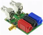
Test #1: Coupling an RF Signal to the IN+ Pin
For testing the IN+ pin the op amp is connected in the unity gain configuration. Applying the RF signal is
straightforward, as it can be connected directly to the IN+ pin. As a result, there are a minimum of
disturbing components in the RF signal path. The circuit diagram is shown in Figure 3. The PCB trace
from RFin to the IN+ pin should be a 50Ω stripline in order to match the RF impedance of the cabling and
the RF generator. On the PCB a 50Ω termination is used. This 50Ω resistor is also used to set the bias
level of the IN+ pin to ground level. The DC measurements are taken at the output of the op amp. As the
op amp is in the unity gain configuration, the input referred offset voltage shift corresponds one-to-one to
the measured output voltage shift.
C2
10 µF
+
VDD
C3
100 pF
RFin
+
R1
50:
OUT
C4
C1
100 pF
22 pF
+
VSS
C5
10 µF
Figure 3. Coupling the RF Signal to the IN+ Pin Circuit Diagram
4.4.3
Test #2: Coupling an RF Signal to the IN− Pin
For coupling an RF signal to the IN− pin, the unity gain configuration as described for the IN+ pin cannot
be used. In that configuration the RF signal would be applied not only to the IN− pin but to the output pin
as well. For accurately measuring the EMIRR of the IN− pin, RF isolation is required for the output pin.
Therefore, a voltage gain configuration is used as shown in Figure 4. The low-frequency gain, which
applies to the resulting offset shift, is set to 2. The feedback resistor R3 and the load capacitance isolate
the output pin from the injected RF signal at the IN− pin.
The gain of the feedback network is not important for the applied RF signal. Since the RF frequency is
much higher than the Gain-Bandwidth-Product (GBP) of the op amp, the op amp configuration can be
seen for RF signals as an open loop circuit. The gain of the op amp configuration is important for
translating the obtained output voltage shift to an input referred offset voltage shift. The input referred
offset voltage shift is calculated by dividing the measured output voltage shift by the voltage gain, which is
2 in this case.
Also for this PCB the signal path from RFin to the IN− pin should be a 50Ω stripline with appropriate
termination. The RF signal is applied to the IN− pin via a coupling capacitor C1. The parasitic series
inductance of this capacitor needs to be compared to the 50Ω impedance of the RF signal path. So, an
inductance of a few nH is acceptable when measuring up to a few GHz. As a result a standard SMD
component can be used here.
For symmetry reasons it is expected that the positive and negative input have the same sensitivity for
applied RF signals but with an opposite polarity for the obtained input referred offset shift. The input pins
thus have the same EMIRR.
6
AN-1698 A Specification for EMI Hardened Operational Amplifiers
SNOA497B – September 2007 – Revised April 2013
Submit Documentation Feedback
Copyright © 2007–2013, Texas Instruments Incorporated
�EMIRR Measurement
www.ti.com
C2
10 µF
+
VDD
C3
100 pF
+
-
C1
RFin
R1
50:
OUT
C6
22 pF
220 pF
R3
1 k:
R2
1 k:
C4
100 pF
+
VSS
C5
10 µF
Figure 4. Coupling the RF Signal to the IN− Pin Circuit Diagram
4.4.4
Test #3 and #4: Coupling an RF Signal to the Supply Pins
For coupling an RF signal to the supply pins, the op amp can again be connected in the unity gain
configuration. A single PCB can serve for measuring the EMIRR for both supply pins, VDD and VSS.
Figure 5 depicts the schematic. On this PCB both RF signal paths from the RF injection point to a supply
pin should be a 50Ω stripline with a 50Ω termination. It is important to remove the decoupling capacitor on
the pin that is under test. Thus, when injecting an RF signal on the VDD pin, capacitor C4 and C5 should be
removed, while capacitor C6 and C7 should be removed when injecting an RF signal on the VSS pin. The
inductors L1 and L2 are used to isolate the power supply sources from the RF signal. This prevents the
sources from detecting the RF signal that might deteriorate the measurement accuracy.
VDD
L1
1 PH
C4
10 PF
+
RFin VDD
Remove when
RF on VDD
C1
R1
100 pF
C5
100 pF
50:
+
OUT
C2
22 pF
C6
10 PF
RFin VSS
+
R2
50:
C3
L2
100 pF 1 PH
VSS
C7
100 pF
Remove when
RF on VSS
Figure 5. Coupling an RF Signal to Either of the Supply Pins Circuit Diagram
SNOA497B – September 2007 – Revised April 2013
Submit Documentation Feedback
AN-1698 A Specification for EMI Hardened Operational Amplifiers
Copyright © 2007–2013, Texas Instruments Incorporated
7
�EMIRR Measurement
4.4.5
www.ti.com
Test #5: Coupling an RF Signal to the Output Pin
Analogous to the circuit for testing the IN− pin, the circuit for testing the output pin requires a voltage gain
configuration. When applying an RF signal to the output pin, the IN− pin needs to be isolated. As the
sensitivity of the output pin is expected to be lower than the sensitivity of the input pin, a better isolation is
needed for this case. The schematic for coupling an RF signal to the output pin is depicted in Figure 6.
The resulting offset shift is again measured at the output. So, the equivalent input referred offset voltage
shift is found by dividing the obtained output voltage shift by the gain of the configuration: 1+(R2+R3)/R1.
Special attention needs to be paid to the isolation of the DC meter connected to the output. As the RF
signal is applied to the same node where the resulting offset voltage shift needs to be measured, a lowpass filter (R5, R6, C7) is placed between the RF injection node and the DC meter. This low-pass filter
prevents the DC meter from detecting the applied RF signal which would directly affect the measurement
results.
C2
220 pF
R4
50:
VDD
C3
10 µF
+
RFin
C4
100 pF
+
R1
100:
R5
R6
10 k:
10 k:
OUT
C7
220 pF
C1
220 pF
R2
4.7 k:
R3
4.7 k:
+
VSS
C5
100 pF
C6
100 pF
Figure 6. Coupling an RF Signal to the Output Pin Circuit Diagram
8
AN-1698 A Specification for EMI Hardened Operational Amplifiers
SNOA497B – September 2007 – Revised April 2013
Submit Documentation Feedback
Copyright © 2007–2013, Texas Instruments Incorporated
�Measurement Results for the LMV851/LMV852/LMV854
www.ti.com
5
Measurement Results for the LMV851/LMV852/LMV854
The five test circuits that are described in Section 4.4 are used to perform EMIRR measurements on the
LMV851. The LMV851 is a single EMI hardened op amp with 8 MHz bandwidth. The supply voltages used
are 2.5V on the positive supply and −2.5V on the negative supply. Measurement results apply to the dual
version, LMV852, and the quad version, LMV854, as well.
To characterize the sensitivity of the various pins two types of measurement results are presented:
• The EMIRR as a function of the frequency of the applied signal. The level of the signal is set to the
standard level of 100 mVP (−20 dBVP).
• The EMIRR as a function of the level of the applied signal. The frequency is set to four typical values:
400 MHz, 900 MHz, 1.8 GHz, and 2.4 GHz.
5.1
EMIRR Vs. Frequency
Figure 7 depicts the EMIRR versus frequency for the various pins. The measurement is performed with a
fixed RF level of −20 dBVP and a varying RF signal frequency. The frequency range is 10 MHz to 1 GHz.
From these results several conclusions can be drawn. First, it is clearly visible that the IN+ and IN− pin do
have the same EMIRR. This was already noticed for reasons of input stage symmetry. Second, the VDD,
VSS and OUT pins have a significantly higher EMIRR than the input pins. This is also quite logical as the
inputs are meant to be sensitive for signals. It should be noted, however, that the supply and output pins
are not generally more robust than the input pins. An op amp needs to be designed specifically for having
high EMIRR for those pins as well.
OUT
EMIRR V_PEAK (dB)
120
100
80
VDD
60
VSS
40
IN+
IN-
20
VPEAK = -20 dBVp
10
100
1000
FREQUENCY (MHz)
10000
Figure 7. EMIRR vs. Frequency for IN+, IN−, VDD, VSS, and OUT
SNOA497B – September 2007 – Revised April 2013
Submit Documentation Feedback
AN-1698 A Specification for EMI Hardened Operational Amplifiers
Copyright © 2007–2013, Texas Instruments Incorporated
9
�Measurement Results for the LMV851/LMV852/LMV854
5.2
www.ti.com
EMIRR Vs. Power
Figure 8 shows the EMIRR as a function of the RF peak level at four typical frequencies.
In Figure 8, two areas can be distinguished. At the left side of the figure, the EMIRR increases as a
function of input level; whereas, at the right side, the EMIRR decreases as a function of the input level.
The left side of the figure is actually an artifact resulting from the limited accuracy of the measurement
setup. For the relatively low input levels, the resulting offset voltage shift is well below the noise level.
Thus, when calculating the EMIRR for that region, the ratio of the input level to the noise level is depicted.
As the noise level is constant for the setup, an increasing EMIRR is obtained for increasing input signal
level.
For the right side, the obtained offset-shift is well above the noise level. As the relation between offset
voltage shift and RF input level is quadratic, the ratio as used in the EMIRR is inversely proportional to the
RF input level, which is in line with the displayed slope of “−1”.
2400 MHz
EMIRR V_PEAK (dB)
100
80
400 MHz
60
900 MHz
40
1800 MHz
20
0
-60
-50
-40
-30
-20
-10
0
10
RF INPUT PEAK VOLTAGE (dBVp)
Figure 8. EMIRR vs. RF Input Peak Level for IN+
10
AN-1698 A Specification for EMI Hardened Operational Amplifiers
SNOA497B – September 2007 – Revised April 2013
Submit Documentation Feedback
Copyright © 2007–2013, Texas Instruments Incorporated
�Typical Applications and EMIRR
www.ti.com
6
Typical Applications and EMIRR
EMI hardened op amps can be used in a wide range of applications. Applications with sensors that
produce relatively low signal levels especially benefit from the EMI robustness. These small signals can
easily be deteriorated by an interfering RF signal. As the small signals require a large gain of the op amp
circuit, the detected RF signals get amplified as well and might introduce a significant error in the overall
signal processing path. An EMI hardened op amp minimizes the effect of interference that, once detected,
propagates into the subsequent circuitry. Two examples are given to demonstrate the advantage of EMI
hardened op amps:
• The first example describes a generic signal path application
• The second example describes a test in which a cell phone interferes with a pressure sensor
application
6.1
Signal Path Application
In Figure 9, a typical signal path application is shown with a sensor, an op amp and an ADC that connects
to a microcontroller. The sensor can be a Ph-sensor or a thermocouple for instance, that produces a
signal which needs to be measured. This signal is amplified by the op amp to match the ADC input range.
Accordingly the ADC digitizes the signal such that it can be read by a microcontroller for further
processing.
Input
VS
+
-
+
RS
SENSOR
ADC
uC
-
R1
R2
100 k:
1 k:
Figure 9. Typical Signal Path Application
Suppose that this application is in an aggressive EM environment and that the interfering signal is mainly
received by the sensor and its wiring. Consequently, an RF signal arrives at the input of the op amp.
Further, assume that the RF signal at the input of the op amp is −20 dBVP at 900 MHz and that the gain of
the op amp configuration is 101x. The ADC used has a 10-bit resolution and a 5V input range. Two
examples will be given to demonstrate the effect an interfering signal can have on the ADC measurement
accuracy and thus on the overall performance.
• First, a standard op amp without any special EMI robustness is used. Such an op amp can have an
EMIRR of 50 dB at 900 MHz, for instance. This means that for this situation the input referred offset
voltage shifts about 0.32 mV as a result of the RF signal of −20 dBVP. As a result of the gain of 101x
the output voltage shift equals 32 mV.
• Second, an LMV851 EMI hardened op amp is placed in the application. The LMV851 has an EMIRR of
about 80 dB at 900 MHz. This results in an input referred offset voltage shift of about 10 µV, which is
equivalent to 1 mV shift at the output.
The ADC has a resolution of 10 bit with a 5V range. This means that one bit corresponds to 5/1024 = 4.88
mV. To be able to use the full measurement resolution without incorrect readings the error signal should
not be larger than half a bit or 2.44 mV. The standard op amp has an output shift of 32 mV, which is
equivalent to about 7 counts. The output shift of 1 mV for the LMV851 EMI hardened op amp is equivalent
to 0.2-bit.
SNOA497B – September 2007 – Revised April 2013
Submit Documentation Feedback
AN-1698 A Specification for EMI Hardened Operational Amplifiers
Copyright © 2007–2013, Texas Instruments Incorporated
11
�Typical Applications and EMIRR
6.2
www.ti.com
Cell Phone Call
The effect of electromagnetic interference is demonstrated in a setup where a cell phone causes
interference with a pressure sensor application (Figure 10). This application needs two op amps and
therefore a dual op amp is used. The experiment is performed on two different dual op amps as in the
previous example: a typical standard op amp and the dual LMV852 EMI hardened op amp. The op amps
are connected to a single supply. The cell phone is placed in a fixed position a couple of centimeters from
the op amps.
When the cell phone is called, the op amps detect the RF signal transmitted by the cell phone. The
resulting effect on the output voltage of the second op amp is depicted in Figure 11.
The difference between the two types of dual op amps is clearly visible. The typical standard dual op amp
has an output voltage shift (disturbing signal) larger than 1V as a result of the RF signal transmitted by the
cell phone. The LMV852 EMI hardened op amp does not show any significant disturbances.
It should be noted that the relative size of the disturbances in the output signal for those two cases, is
equal to the difference of the EMIRR for the two dual op amps used. So, the EMIRR enables an early
selection of components for building an EMI robust application.
R1
1.5 k:
VDD
PRESSURE
SENSOR
+
-
Opamp1
-
VDD
R2
100:
+
ADC
Opamp2
+
VOUT
VS
VOUT (0.5V/DIV)
Figure 10. Pressure Sensor Application
Typical Opamp
LMV852
TIME (0.5s/DIV)
Figure 11. Comparing EMI Robustness
12
AN-1698 A Specification for EMI Hardened Operational Amplifiers
SNOA497B – September 2007 – Revised April 2013
Submit Documentation Feedback
Copyright © 2007–2013, Texas Instruments Incorporated
�IMPORTANT NOTICE
Texas Instruments Incorporated and its subsidiaries (TI) reserve the right to make corrections, enhancements, improvements and other
changes to its semiconductor products and services per JESD46, latest issue, and to discontinue any product or service per JESD48, latest
issue. Buyers should obtain the latest relevant information before placing orders and should verify that such information is current and
complete. All semiconductor products (also referred to herein as “components”) are sold subject to TI’s terms and conditions of sale
supplied at the time of order acknowledgment.
TI warrants performance of its components to the specifications applicable at the time of sale, in accordance with the warranty in TI’s terms
and conditions of sale of semiconductor products. Testing and other quality control techniques are used to the extent TI deems necessary
to support this warranty. Except where mandated by applicable law, testing of all parameters of each component is not necessarily
performed.
TI assumes no liability for applications assistance or the design of Buyers’ products. Buyers are responsible for their products and
applications using TI components. To minimize the risks associated with Buyers’ products and applications, Buyers should provide
adequate design and operating safeguards.
TI does not warrant or represent that any license, either express or implied, is granted under any patent right, copyright, mask work right, or
other intellectual property right relating to any combination, machine, or process in which TI components or services are used. Information
published by TI regarding third-party products or services does not constitute a license to use such products or services or a warranty or
endorsement thereof. Use of such information may require a license from a third party under the patents or other intellectual property of the
third party, or a license from TI under the patents or other intellectual property of TI.
Reproduction of significant portions of TI information in TI data books or data sheets is permissible only if reproduction is without alteration
and is accompanied by all associated warranties, conditions, limitations, and notices. TI is not responsible or liable for such altered
documentation. Information of third parties may be subject to additional restrictions.
Resale of TI components or services with statements different from or beyond the parameters stated by TI for that component or service
voids all express and any implied warranties for the associated TI component or service and is an unfair and deceptive business practice.
TI is not responsible or liable for any such statements.
Buyer acknowledges and agrees that it is solely responsible for compliance with all legal, regulatory and safety-related requirements
concerning its products, and any use of TI components in its applications, notwithstanding any applications-related information or support
that may be provided by TI. Buyer represents and agrees that it has all the necessary expertise to create and implement safeguards which
anticipate dangerous consequences of failures, monitor failures and their consequences, lessen the likelihood of failures that might cause
harm and take appropriate remedial actions. Buyer will fully indemnify TI and its representatives against any damages arising out of the use
of any TI components in safety-critical applications.
In some cases, TI components may be promoted specifically to facilitate safety-related applications. With such components, TI’s goal is to
help enable customers to design and create their own end-product solutions that meet applicable functional safety standards and
requirements. Nonetheless, such components are subject to these terms.
No TI components are authorized for use in FDA Class III (or similar life-critical medical equipment) unless authorized officers of the parties
have executed a special agreement specifically governing such use.
Only those TI components which TI has specifically designated as military grade or “enhanced plastic” are designed and intended for use in
military/aerospace applications or environments. Buyer acknowledges and agrees that any military or aerospace use of TI components
which have not been so designated is solely at the Buyer's risk, and that Buyer is solely responsible for compliance with all legal and
regulatory requirements in connection with such use.
TI has specifically designated certain components as meeting ISO/TS16949 requirements, mainly for automotive use. In any case of use of
non-designated products, TI will not be responsible for any failure to meet ISO/TS16949.
Products
Applications
Audio
www.ti.com/audio
Automotive and Transportation
www.ti.com/automotive
Amplifiers
amplifier.ti.com
Communications and Telecom
www.ti.com/communications
Data Converters
dataconverter.ti.com
Computers and Peripherals
www.ti.com/computers
DLP® Products
www.dlp.com
Consumer Electronics
www.ti.com/consumer-apps
DSP
dsp.ti.com
Energy and Lighting
www.ti.com/energy
Clocks and Timers
www.ti.com/clocks
Industrial
www.ti.com/industrial
Interface
interface.ti.com
Medical
www.ti.com/medical
Logic
logic.ti.com
Security
www.ti.com/security
Power Mgmt
power.ti.com
Space, Avionics and Defense
www.ti.com/space-avionics-defense
Microcontrollers
microcontroller.ti.com
Video and Imaging
www.ti.com/video
RFID
www.ti-rfid.com
OMAP Applications Processors
www.ti.com/omap
TI E2E Community
e2e.ti.com
Wireless Connectivity
www.ti.com/wirelessconnectivity
Mailing Address: Texas Instruments, Post Office Box 655303, Dallas, Texas 75265
Copyright © 2013, Texas Instruments Incorporated
�