OBSOLETE
LMX2324
www.ti.com
SNAS038D – NOVEMBER 1999 – REVISED MARCH 2013
LMX2324 PLLatinum™ 2.0 GHz Frequency Synthesizer for RF Personal Communications
Check for Samples: LMX2324
FEATURES
DESCRIPTION
•
•
•
The LMX2324 is a high performance frequency
synthesizer with integrated 32/33 dual modulus
prescaler designed for RF operation up to 2.0 GHz.
Using a proprietary digital phase locked loop
technique, the LMX2324's linear phase detector
characteristics can generate very stable, low noise
control signals for UHF and VHF voltage controlled
oscillators.
1
23
•
•
RF Operation up to 2.0 GHz
2.7V to 5.5V Operation
Low Current Consumption: ICC = 3.5 mA (typ)
at VCC = 3.0V
Dual Modulus Prescaler: 32/33
Internal Balanced, Low Leakage Charge Pump
APPLICATIONS
•
•
•
•
Cellular Telephone Systems (GSM, NADC,
CDMA, PDC)
Personal Wireless Communications (DCS1800, DECT, CT-1+)
Wireless Local Area Networks (WLANs)
Other Wireless Communication Systems
Serial data is transferred into the LMX2324 via a
three-line MICROWIRE interface (Data, LE, Clock).
Supply voltage range is from 2.7V to 5.5V. The
LMX2324 features very low current consumption,
typically 3.5 mA at 3V. The charge pump provides 4
mA output current.
The LMX2324 is manufactured using TI's ABiC V
BiCMOS process and is packaged in a 16-pin
TSSOP and a 16-pin PLGA package.
Functional Block Diagram
1
2
3
Please be aware that an important notice concerning availability, standard warranty, and use in critical applications of
Texas Instruments semiconductor products and disclaimers thereto appears at the end of this data sheet.
PLLatinum is a trademark of Texas Instruments.
All other trademarks are the property of their respective owners.
PRODUCTION DATA information is current as of publication date.
Products conform to specifications per the terms of the Texas
Instruments standard warranty. Production processing does not
necessarily include testing of all parameters.
Copyright © 1999–2013, Texas Instruments Incorporated
�OBSOLETE
LMX2324
SNAS038D – NOVEMBER 1999 – REVISED MARCH 2013
www.ti.com
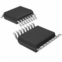
Connection Diagram
Figure 1. TSSOP 16-Pin Package
See Package Number PW0016A
Figure 2. PLGA 16-Pin Package
See Package Number NPG0016A
PIN DESCRIPTIONS
Pin No.
Pin
Name
I/O
1
VP
—
Power supply for charge pump. Must be ≥ VCC
2
CPo
O
Internal charge pump output. For connection to a loop filter for driving the voltage
control input of an external oscillator.
4
3
GND
—
Ground.
5
4
fINB
I
RF prescaler complimentary input. In single-ended mode, a bypass capacitor should
be placed as close as possible to this pin and be connected directly to the ground
plane. The LMX2324 can be driven differentially when the bypass capacitor is omitted.
6
5
fIN
I
RF prescaler input. Small signal input from the voltage controlled oscillator.
7
6
NC
8
7
NC
9
8
OSCin
TSSOP16
PLGA16
2
3
Description
No Connect
No Connect
I
Oscillator input. A CMOS inverting gate input. The input has a VCC/2 input threshold
and can be driven from an external CMOS or TTL logic gate.
10
9
NC
12
10
Clock
I
No Connect
High impedance CMOS Clock input. Data is clocked in on the rising edge, for the
various counters and registers.
13
11
Data
I
Binary serial data input. Data entered MSB first. LSB is control bit. High impedance
CMOS input.
14
12
LE
I
Load Enable input. When Load Enable transitions HIGH, data is loaded into either the
N or R register (control bit dependent). See Serial Data Input Timing.
15
13
NC
11
14
NC
16
15
CE
I
CHIP Enable. A LOW on CE powers down the device asynchronously and will TRISTATE the charge pump output.
1
16
VCC
I
Power supply voltage input. Input may range from 2.7V to 5.5V. Bypass capacitors
should be placed as close as possible to this pin and be connected directly to the
ground plane.
No Connect
No Connect
These devices have limited built-in ESD protection. The leads should be shorted together or the device placed in conductive foam
during storage or handling to prevent electrostatic damage to the MOS gates.
2
Submit Documentation Feedback
Copyright © 1999–2013, Texas Instruments Incorporated
Product Folder Links: LMX2324
�OBSOLETE
LMX2324
www.ti.com
SNAS038D – NOVEMBER 1999 – REVISED MARCH 2013
Absolute Maximum Ratings (1) (2) (3)
−0.3V to 6.5V
Power Supply Voltage (VCC)
Power Supply for Charge Pump (VP)
VCC to 6.5V
Voltage on Any Pin with
−0.3V to VCC + 0.3V
GND = 0V (VI)
−65°C to +150°C
Storage Temperature Range (TS)
Lead Temperature (solder, 4 sec.) (TL)
(1)
+260°C
Absolute Maximum Ratings indicate limits beyond which damage to the device may occur. Recommended Operating Conditions indicate
conditions for which the device is intended to be functional, but do not ensure specific performance limits. For ensured specifications
and test conditions, see the Electrical Characteristics.
This device is a high performance RF integrated circuit with an ESD rating < 2kV. and is ESD sensitive. Handling and assembly of this
device should on be done on ESD protected workstations.
If Military/Aerospace specified devices are required, please contact the TI Sales Office/ Distributors for availability and specifications.
(2)
(3)
Recommended Operating Conditions
(1)
Power Supply Voltage (VCC)
2.7V to 5.5V
Power Supply for Charge Pump (VP)
VCC to 5.5V
−40°C to +85°C
Operating Temperature (TA)
(1)
Absolute Maximum Ratings indicate limits beyond which damage to the device may occur. Recommended Operating Conditions indicate
conditions for which the device is intended to be functional, but do not ensure specific performance limits. For ensured specifications
and test conditions, see the Electrical Characteristics.
Electrical Characteristics
(VCC = 3V, VP = 3V; −40°C < TA < 85°C except as specified).
All min/max specifications are ensured by design, or test, or statistical methods.
Symbol
Parameter
Conditions
Min
Typ
Max
Units
GENERAL
ICC
Power Supply Current
ICC-PWDN
Power Down Current
fIN
fIN Operating Frequency
OSCin
Oscillator Operating Frequency
fPD
Phase Detector Frequency
PfIN
Input Sensitivity fINB grounded through a 10
pF capacitor
VOSC
VCC = 2.7V to 5.5V
3.5
mA
10
µA
0.1
2.0
GHz
5
40
MHz
10
MHz
VCC = 3.0V
−15
0
VCC = 5.0V
−10
0
Oscillator Sensitivity
0.4
1.0
VCC−0.3
dBm
VPP
CHARGE PUMP
ICPo-source
Charge Pump Output Current
VCPo = VP/2
ICPo-sink
−4.0
mA
4.0
mA
ICPo-Tri
Charge Pump TRI-STATE Current
0.5 ≤ VCPo ≤ VP - 0.5
T = 25°C
0.1
nA
ICPo vs.
VCPo
Charge Pump Output Current Variation vs.
Voltage (1)
0.5 ≤ VCPo ≤ VP - 0.5
T = 25°C
10
%
ICPo-sink vs.
ICPo-source
Charge Pump Output Current Sink vs.
Source Mismatch (1)
VCPo = VP/2
T = 25°C
5
%
ICPo vs. T
Charge Pump Output Current Magnitude
Variation vs. Temperature (1)
VCPo = VP/2
−40°C ≤ T ≤ +85°C
10
%
(1)
See related equations in Charge Pump Current Specification Definitions
Submit Documentation Feedback
Copyright © 1999–2013, Texas Instruments Incorporated
Product Folder Links: LMX2324
3
�OBSOLETE
LMX2324
SNAS038D – NOVEMBER 1999 – REVISED MARCH 2013
www.ti.com
Electrical Characteristics (continued)
(VCC = 3V, VP = 3V; −40°C < TA < 85°C except as specified).
All min/max specifications are ensured by design, or test, or statistical methods.
Symbol
Parameter
Conditions
Min
Typ
Max
Units
DIGITAL INTERFACE (DATA, CLK, LE, CE)
VIH
High-Level Input Voltage
(2)
VIL
Low-Level Input Voltage
(2)
IIH
High-Level Input Current
VIH = VCC = 5.5V
IIL
Low-Level Input Current
VIL = 0, VCC = 5.5V
IIH
Oscillator Input Current
VIH = VCC = 5.5V
IIL
VIL = 0, VCC = 5.5V
0.8 VCC
V
0.2 VCC
V
−1.0
1.0
µA
−1.0
1.0
µA
100
µA
−100
µA
MICROWIRE TIMING
tCS
Data to Clock Set Up Time
See Data Input Timing
50
ns
tCH
Data to Clock Hold Time
See Data Input Timing
10
ns
tCWH
Clock Pulse Width High
See Data Input Timing
50
ns
tCWL
Clock Pulse Width Low
See Data Input Timing
50
ns
tES
Clock to Enable Set Up Time
See Data Input Timing
50
ns
tEW
Enable Pulse Width
See Data Input Timing
50
ns
(2)
Except fIN and OSCin
Charge Pump Current Specification Definitions
I1 = CP sink current at VCPo = VP − ΔV
I2 = CP sink current at VCPo = VP/2
I3 = CP sink current at VCPo = ΔV
I4 = CP source current at VCPo = VP − ΔV
I5 = CP source current at VCPo = VP/2
I6 = CP source current at VCPo = ΔV
ΔV = Voltage offset from positive and negative rails. Dependent on VCO tuning range relative to VP and ground.
Typical values are between 0.5V and 1.0V.
1. ICPo vs. VCPo = Charge Pump Output Current magnitude variation vs. Voltage =
[½ * {|I1| − |I3|}]/[½ * {|I1| + |I3|}] * 100% and [½ * {|I4| − |I6|}]/[½ * {|I4| + |I6|}] * 100%
2. ICPo-sink vs. ICPo-source = Charge Pump Output Current Sink vs. Source Mismatch =
[|I2| − |I5|]/[½ * {|I2| + |I5|}] * 100%
3. ICPo vs. T = Charge Pump Output Current magnitude variation vs. Temperature =
[|I2 @ temp| − |I2 @ 25°C|]/|I2 @ 25°C| * 100% and [|I5 @ temp| − |I5 @ 25°C|]/|I5 @ 25°C| * 100%
4
Submit Documentation Feedback
Copyright © 1999–2013, Texas Instruments Incorporated
Product Folder Links: LMX2324
�OBSOLETE
LMX2324
www.ti.com
SNAS038D – NOVEMBER 1999 – REVISED MARCH 2013
FUNCTIONAL DESCRIPTION
The basic phase-lock-loop (PLL) configuration consists of a high-stability crystal reference oscillator, a frequency
synthesizer such as the Texas Instruments LMX2324, a voltage controlled oscillator (VCO), and a passive loop
filter. The frequency synthesizer includes a phase detector, current mode charge pump, as well as
programmable reference [R] and feedback [N] frequency dividers. The VCO frequency is established by dividing
the crystal reference signal down via the R counter to obtain a frequency that sets the comparison frequency.
This reference signal, fr, is then presented to the input of a phase/frequency detector and compared with another
signal, fp, the feedback signal, which was obtained by dividing the VCO frequency down by way of the N counter.
The phase/frequency detector's current source outputs pump charge into the loop filter, which then converts the
charge into the VCO's control voltage. The phase/frequency comparator's function is to adjust the voltage
presented to the VCO until the feedback signal's frequency (and phase) match that of the reference signal. When
this “phase-locked” condition exists, the RF VCO's frequency will be N times that of the comparison frequency,
where N is the divider ratio.
OSCILLATOR
The reference oscillator frequency for the PLL is provided by an external reference TCXO through the OSCin pin.
OSCin block can operate to 40 MHz with a minimum input sensitivity of 0.4VPP. The inputs have a VCC/2 input
threshold and can be driven from an external CMOS or TTL logic gate.
REFERENCE DIVIDERS (R COUNTER)
The R Counter is clocked through the oscillator block. The maximum frequency is 40 MHz. The R Counter is a
10 bit CMOS binary counter with a divide range from 2 to 1,023. See 10-Bit Programmable Reference Divider
Ratio (R Counter).
PROGRAMMABLE DIVIDERS (N COUNTER)
The N counter is clocked by the small signal fIN and fINB input pins. The LMX2324 RF N counter is 15 bit integer
divider. The N counter is configured as a 5 bit A Counter and a 10 bit B Counter, offering a continuous integer
divide range from 992 to 32,767. The LMX2324 is capable of operating from 100 MHz to 2.0 GHz with a 32/33
prescaler.
Prescaler
The RF inputs to the prescaler consist of the fIN and fINB pins which are the complimentary inputs of a differential
pair amplifier. The differential fIN configuration can operate to 2 GHz with an input sensitivity of −15 dBm. The
input buffer drives the N counter's ECL D-type flip flops in a dual modulus configuration. A 32/33 prescale ratio is
provided for the LMX2324. The prescaler clocks the subsequent CMOS flip-flop chain comprising the fully
programmable A and B counters.
PHASE/FREQUENCY DETECTOR
The phase(/frequency) detector is driven from the N and R counter outputs. The maximum frequency at the
phase detector inputs is 10 MHz. The phase detector outputs control the charge pumps. The polarity of the
pump-up or pump-down control is programmed using PD_POL, depending on whether RF VCO characteristics
are positive or negative (see R Register Truth Table). The phase detector also receives a feedback signal from
the charge pump, in order to eliminate dead zone.
CHARGE PUMP
The phase detector's current source output pumps charge into an external loop filter, which then converts the
charge into the VCO's control voltage. The charge pumps steer the charge pump output, CPo, to VP (pump-up) or
Ground (pump-down). When locked, CPo is primarily in a TRI-STATE mode with small corrections. The RF
charge pump output current magnitude is set to 4.0 mA. The charge pump output can also be used to output
divider signals as detailed in Test Mode Truth Table (R[13] = 1).
Submit Documentation Feedback
Copyright © 1999–2013, Texas Instruments Incorporated
Product Folder Links: LMX2324
5
�OBSOLETE
LMX2324
SNAS038D – NOVEMBER 1999 – REVISED MARCH 2013
www.ti.com
MICROWIRE SERIAL INTERFACE
The programmable functions are accessed through the MICROWIRE serial interface. The interface is made of
three functions: clock, data and latch enable (LE). Serial data for the various counters is clocked in from data on
the rising edge of clock, into the 18-bit shift register. Data is entered MSB first. The last bit decodes the internal
register address. On the rising edge of LE, data stored in the shift register is loaded into one of the two
appropriate latches (selected by address bits). A complete programming description is included in the following
sections.
POWER CONTROL
The PLL can be power controlled in two ways. The first method is by setting the CE pin LOW. This
asynchronously powers down the PLL and TRI-STATE the charge pump output, regardless of the PWDN bit
status. The second method is by programming through MICROWIRE, while keeping the CE HIGH. Programming
the PWDN bit in the N register HIGH (CE=HIGH) will disable the N counter and de-bias the fIN input (to a high
impedance state). The R counter functionality also becomes disabled. The reference oscillator block powers
down when the power down bit is asserted. The OSCin pin reverts to a high impedance state when this condition
exists. Power down forces the charge pump and phase comparator logic to a TRI-STATE condition. A power
down counter reset function resets both N and R counters. Upon powering up the N counter resumes counting in
“close” alignment with the R counter (The maximum error is one prescaler cycle). The MICROWIRE control
register remains active and capable of loading and latching in data during all of the power down modes.
Programming Description
MICROWIRE INTERFACE
The LMX2324 register set can be accessed through the MICROWIRE interface. A 18-bit shift register is used as
a temporary register to indirectly program the on-chip registers. The shift register consists of a 17-bit DATA[16:0]
field and a 1-bit address (ADDR) field as shown below. The address field is used to decode the internal register
address. Data is clocked into the shift register in the direction from MSB to LSB, when the CLOCK signal goes
high. On the rising edge of Load Enable (LE) signal, data stored in the shift register is loaded into the addressed
latch.
MSB
LSB
DATA[16:0]
ADDR
17
1
0
Registers' Address Map
When Load Enable (LE) is transitioned high, data is transferred from the 18-bit shift register into the appropriate
latch depending on the state of the ADDRESS bit. A multiplexing circuit decodes the address bit and writes the
data field to the corresponding internal register.
REGISTER
ADDRESSED
ADDRESS BIT
ADDR
R Register
1
N Register
0
Register Content Truth Table
MSB
17
SHIFT REGISTER BIT LOCATION
16
15
14
13
12
11
10
9
8
7
6
LSB
5
4
3
1
Data Field
Register
NB_CNTR[9:0]
NA_CNTR[4:0]
N16
N15
N14
N13
N12
N11
N10
X
X
X
TES
T
RS
PD_
POL
CP_
TRI
R16
R15
R14
R13
R12
R11
R10
R
N9
N8
0
ADDR
Field
CTL_WORD[1:0
]
N
6
2
N7
N6
N5
N4
N3
N2
N1
N0
R3
R2
R1
R0
0
R_CNTR[9:0]
1
R9
R8
R7
R6
Submit Documentation Feedback
R5
R4
Copyright © 1999–2013, Texas Instruments Incorporated
Product Folder Links: LMX2324
�OBSOLETE
LMX2324
www.ti.com
SNAS038D – NOVEMBER 1999 – REVISED MARCH 2013
R REGISTER
If the Address Bit (ADDR) is 1, when LE is transitioned high data is transferred from the 18-bit shift register into
the 14-bit R register. The R register contains a latch which sets the PLL 10-bit R counter divide ratio. The divide
ratio is programmed using the bits R_CNTR as shown in 10-Bit Programmable Reference Divider Ratio (R
Counter). The ratio must be ≥ 2. The PD_POL, CP_TRI and TEST bits control the phase detector polarity,
charge pump TRI-STATE, and test mode respectively, as shown in R Register Truth Table. The RS bit is
reserved and should always be set to zero. X denotes a don't care condition. Data is clocked into the shift
register MSB first.
MSB
SHIFT REGISTER BIT LOCATION
17
16
15
14
13
12
11
10
Register
9
8
7
LSB
6
5
4
3
2
1
Data Field
X
X
X
TES
T
RS
PD_
POL
CP_
TRI
R16
R15
R14
R13
R12
R11
R10
R
0
ADDR
Field
R_CNTR[9:0]
1
R9
R8
R7
R6
R5
R4
R3
R2
R1
R0
10-Bit Programmable Reference Divider Ratio (R Counter) (1)
R_CNTR[9:0]
(1)
Divide
Ratio
R9
R8
R7
R6
R5
R4
R3
R2
R1
R0
2
0
0
0
0
0
0
0
0
1
0
3
0
0
0
0
0
0
0
0
1
1
•
•
•
•
•
•
•
•
•
•
•
1,023
1
1
1
1
1
1
1
1
1
1
Notes: Divide ratio: 2 to 1,023 (Divide ratios less than 2 are prohibited)
R_CNTR—These bits select the divide ratio of the programmable reference dividers.
R Register Truth Table
Bit
Location
Function
0
1
CP_TRI
R[10]
Charge Pump TRI-STATE Normal Operation
TRI-STATE
PD_POL
R[11]
Phase Detector Polarity
Negative
Positive
TEST
R[13]
Test Mode Bit
Normal Operation
Test Mode
If the test mode is NOT activated (R[13]=0), the charge pump is active when CP_TRI is set LOW. When CP_TRI
is set HIGH, the charge pump output and phase comparator are forced to a TRI-STATE condition. This bit must
be set HIGH if the test mode is ACTIVATED (R[13]=1).
If the test mode is NOT activated (R[13]=0), PD_POL sets the VCO characteristics to positive when set HIGH.
When PD_POL is set LOW, the VCO exhibits a negative characteristic where the VCO frequency decreases with
increasing control voltage.
If the test mode is ACTIVATED (R[13]=1), the outputs of the N and R counters are directed to the CPo output to
allow for testing. The PD_POL bit selects which counter output according to Test Mode Truth Table (R[13] = 1).
Test Mode Truth Table (R[13] = 1)
CP_TRI R[10]
PD_POL R[11]
R Divider Output
CPo Output
1
0
N Divider Output
1
1
Submit Documentation Feedback
Copyright © 1999–2013, Texas Instruments Incorporated
Product Folder Links: LMX2324
7
�OBSOLETE
LMX2324
SNAS038D – NOVEMBER 1999 – REVISED MARCH 2013
www.ti.com
N REGISTER
If the address bit is LOW (ADDR=0) when LE is transitioned high, data is transferred from the 18-bit shift register
into the 17-bit N register. The N register consists of the 5-bit swallow counter (A counter), the 10-bit
programmable counter (B counter) and the control word. Serial data format is shown below in 5-Bit Swallow
Counter Divide Ratio (A Counter) and 10-Bit Programmable Counter Divide Ratio (B Counter). The pulse swallow
function which determines the divide ratio is described in Pulse Swallow Function. Data is clocked into the shift
register MSB first.
MSB
SHIFT REGISTER BIT LOCATION
17
16
15
14
13
12
11
10
Register
9
8
7
LSB
6
5
4
3
2
1
0
Data Field
ADDR
Field
NB_CNTR[9:0]
NA_CNTR[4:0]
CTL_WOR
D[1:0]
N
N16
N15
N14
N13
N12
N11
N10
N9
N8
N7
N6
N5
N4
N3
N2
N1
0
N0
5-Bit Swallow Counter Divide Ratio (A Counter) (1)
Swallow Count
(1)
NA_CNTR[4:0]
(A)
N6
N5
N4
N3
N2
0
0
0
0
0
0
1
0
0
0
0
1
•
•
•
•
•
•
31
1
1
1
1
1
Notes: Swallow Counter Value: 0 to 31
NB_CNTR ≥ NA_CNTR
10-Bit Programmable Counter Divide Ratio (B Counter) (1)
NB_CNTR[10:0]
(1)
Divide
Ratio
N16
N15
N14
N13
N12
N11
N10
N9
N8
N7
3
0
0
0
0
0
0
0
0
1
1
4
0
0
0
0
0
0
0
1
0
0
•
•
•
•
•
•
•
•
•
•
•
1023
1
1
1
1
1
1
1
1
1
1
Notes: Divide ratio: 3 to 1,023 (Divide ratios less than 3 are prohibited)
NB_CNTR ≥ NA_CNTR
Pulse Swallow Function
The N divider counts such that it divides the VCO RF frequency by (P+1) A times, and then divides by P (B - A)
times. The B value (NB_CNTR) must be ≥ 3. The continuous divider ratio is from 992 to 32,767. Divider ratios
less than 992 are achievable as long as the binary counter value is greater than the swallow counter value
(NB_CNTR ≥ NA_CNTR).
fVCO = N x (fOSC/R)
N = (P x B) + A
fVCO: Output frequency of external voltage controlled oscillator (VCO)
fOSC: Output frequency of the external reference frequency oscillator
R:
Preset divide ratio of binary 10-bit programmable reference counter (2 to 1023)
N:
Preset divide ratio of main 15-bit programmable integer N counter (992 to 32,767)
8
Submit Documentation Feedback
Copyright © 1999–2013, Texas Instruments Incorporated
Product Folder Links: LMX2324
�OBSOLETE
LMX2324
www.ti.com
SNAS038D – NOVEMBER 1999 – REVISED MARCH 2013
B:
Preset divide ratio of binary 10-bit programmable B counter (3 to 1023)
A:
Preset value of binary 5-bit swallow A counter (0 ≤ A ≤ 31, A ≤ B)
P:
Preset modulus of dual modulus prescaler (P=32)
CTL_WORD
MSB
LSB
N1
N0
CNT_RST
PWDN
Control Word Truth Table (1)
(1)
CE
CNT_RST
PWDN
Function
1
0
0
Normal Operation
1
0
1
Synchronous Powerdown
1
1
0
Counter Reset
1
1
1
Asynchronous Powerdown
0
X
X
Asynchronous Powerdown
Notes: X denotes don't care.
The Counter Reset enable bit when activated allows the reset of both N and R counters. Upon powering up the
N counter resumes counting in “close” alignment with the R counter. (The maximum error is one prescaler cycle).
Both synchronous and asynchronous power down modes are available with the LMX2324 to be able to adapt to
different types of applications. The MICROWIRE control register remains active and capable of loading and
latching in data during all of the powerdown modes.
Synchronous Power down Mode
The PLL loops can be synchronously powered down by setting the counter reset mode bit to LOW (N[1] = 0) and
its power down mode bit to HIGH (N[0] = 1). The power down function is gated by the charge pump. Once the
power down mode and counter reset mode bits are loaded, the part will go into power down mode upon the
completion of a charge pump pulse event.
Asynchronous Power down Mode
The PLL loops can be asynchronously powered down by setting the counter reset mode bit to HIGH (N[1] = 1)
and its power down mode bit to HIGH (N[0] = 1), or by setting CE pin LOW. The power down function is NOT
gated by the charge pump. Once the power down and counter reset mode bits are loaded, the part will go into
power down mode immediately.
The R and N counters are disabled and held at load point during the synchronous and asynchronous power
down modes. This will allow a smooth acquisition of the RF signal when the PLL is programmed to power up.
Upon powering up, both R and N counters will start at the ‘zero' state, and the relationship between R and N will
not be random.
Submit Documentation Feedback
Copyright © 1999–2013, Texas Instruments Incorporated
Product Folder Links: LMX2324
9
�OBSOLETE
LMX2324
SNAS038D – NOVEMBER 1999 – REVISED MARCH 2013
www.ti.com
Serial Data Input Timing
Notes: Parenthesis data indicates programmable reference divider data.
Data shifted into register on clock rising edge.
Data is shifted in MSB first.
Test Conditions: The Serial Data Input Timing is tested using a symmetrical waveform around VCC/2. The test
waveform has an edge rate of 0.6 V/ns with amplitudes of 1.6V @ VCC = 2.7V and 3.3V @ VCC = 5.5V.
Phase Comparator and Internal Charge Pump Characteristics
Notes: Phase difference detection range: −2π to +2π
The minimum width pump up and pump down current pulses occur at the CPo pin when the loop is locked. PD_POL =
1
fR: Phase comparator input from the R Divider
fN: Phase comparator input from the N divider
CPo: Charge pump output
10
Submit Documentation Feedback
Copyright © 1999–2013, Texas Instruments Incorporated
Product Folder Links: LMX2324
�OBSOLETE
LMX2324
www.ti.com
SNAS038D – NOVEMBER 1999 – REVISED MARCH 2013
REVISION HISTORY
Changes from Revision C (March 2013) to Revision D
•
Page
Changed layout of National Data Sheet to TI format .......................................................................................................... 10
Submit Documentation Feedback
Copyright © 1999–2013, Texas Instruments Incorporated
Product Folder Links: LMX2324
11
�IMPORTANT NOTICE
Texas Instruments Incorporated and its subsidiaries (TI) reserve the right to make corrections, enhancements, improvements and other
changes to its semiconductor products and services per JESD46, latest issue, and to discontinue any product or service per JESD48, latest
issue. Buyers should obtain the latest relevant information before placing orders and should verify that such information is current and
complete. All semiconductor products (also referred to herein as “components”) are sold subject to TI’s terms and conditions of sale
supplied at the time of order acknowledgment.
TI warrants performance of its components to the specifications applicable at the time of sale, in accordance with the warranty in TI’s terms
and conditions of sale of semiconductor products. Testing and other quality control techniques are used to the extent TI deems necessary
to support this warranty. Except where mandated by applicable law, testing of all parameters of each component is not necessarily
performed.
TI assumes no liability for applications assistance or the design of Buyers’ products. Buyers are responsible for their products and
applications using TI components. To minimize the risks associated with Buyers’ products and applications, Buyers should provide
adequate design and operating safeguards.
TI does not warrant or represent that any license, either express or implied, is granted under any patent right, copyright, mask work right, or
other intellectual property right relating to any combination, machine, or process in which TI components or services are used. Information
published by TI regarding third-party products or services does not constitute a license to use such products or services or a warranty or
endorsement thereof. Use of such information may require a license from a third party under the patents or other intellectual property of the
third party, or a license from TI under the patents or other intellectual property of TI.
Reproduction of significant portions of TI information in TI data books or data sheets is permissible only if reproduction is without alteration
and is accompanied by all associated warranties, conditions, limitations, and notices. TI is not responsible or liable for such altered
documentation. Information of third parties may be subject to additional restrictions.
Resale of TI components or services with statements different from or beyond the parameters stated by TI for that component or service
voids all express and any implied warranties for the associated TI component or service and is an unfair and deceptive business practice.
TI is not responsible or liable for any such statements.
Buyer acknowledges and agrees that it is solely responsible for compliance with all legal, regulatory and safety-related requirements
concerning its products, and any use of TI components in its applications, notwithstanding any applications-related information or support
that may be provided by TI. Buyer represents and agrees that it has all the necessary expertise to create and implement safeguards which
anticipate dangerous consequences of failures, monitor failures and their consequences, lessen the likelihood of failures that might cause
harm and take appropriate remedial actions. Buyer will fully indemnify TI and its representatives against any damages arising out of the use
of any TI components in safety-critical applications.
In some cases, TI components may be promoted specifically to facilitate safety-related applications. With such components, TI’s goal is to
help enable customers to design and create their own end-product solutions that meet applicable functional safety standards and
requirements. Nonetheless, such components are subject to these terms.
No TI components are authorized for use in FDA Class III (or similar life-critical medical equipment) unless authorized officers of the parties
have executed a special agreement specifically governing such use.
Only those TI components which TI has specifically designated as military grade or “enhanced plastic” are designed and intended for use in
military/aerospace applications or environments. Buyer acknowledges and agrees that any military or aerospace use of TI components
which have not been so designated is solely at the Buyer's risk, and that Buyer is solely responsible for compliance with all legal and
regulatory requirements in connection with such use.
TI has specifically designated certain components as meeting ISO/TS16949 requirements, mainly for automotive use. In any case of use of
non-designated products, TI will not be responsible for any failure to meet ISO/TS16949.
Products
Applications
Audio
www.ti.com/audio
Automotive and Transportation
www.ti.com/automotive
Amplifiers
amplifier.ti.com
Communications and Telecom
www.ti.com/communications
Data Converters
dataconverter.ti.com
Computers and Peripherals
www.ti.com/computers
DLP® Products
www.dlp.com
Consumer Electronics
www.ti.com/consumer-apps
DSP
dsp.ti.com
Energy and Lighting
www.ti.com/energy
Clocks and Timers
www.ti.com/clocks
Industrial
www.ti.com/industrial
Interface
interface.ti.com
Medical
www.ti.com/medical
Logic
logic.ti.com
Security
www.ti.com/security
Power Mgmt
power.ti.com
Space, Avionics and Defense
www.ti.com/space-avionics-defense
Microcontrollers
microcontroller.ti.com
Video and Imaging
www.ti.com/video
RFID
www.ti-rfid.com
OMAP Applications Processors
www.ti.com/omap
TI E2E Community
e2e.ti.com
Wireless Connectivity
www.ti.com/wirelessconnectivity
Mailing Address: Texas Instruments, Post Office Box 655303, Dallas, Texas 75265
Copyright © 2013, Texas Instruments Incorporated
�


 工商网监
湘ICP备2023018690号
工商网监
湘ICP备2023018690号
