February 2001
LMX2335L/LMX2336L
LMX2335L
1.1 GHz/1.1 GHz
LMX2336L
2.0 GHz/1.1 GHz
PLLatinum™ Low Power Dual Frequency Synthesizer for
RF Personal Communications
General Description
Features
The LMX2335L and LMX2336L are monolithic, integrated
dual frequency synthesizers, including two high frequency
prescalers, and are designed for applications requiring two
RF phase-lock loops. They are fabricated using National’s
0.5µ ABiC V silicon BiCMOS process.
The LMX2335L/36L contains two dual modulus prescalers. A
64/65 or a 128/129 prescaler can be selected for each RF
synthesizer. A second reference divider chain is included in
the IC for improved system noise. The LMX2335L/36L combined with a high quality reference oscillator, two loop filters,
and two external voltage controlled oscillators generates
very stable low noise RF local oscillator signals.
Serial data is transferred into the LMX2335L/36L via a three
wire interface (Data, Enable, Clock). Supply voltage can
range from 2.7V to 5.5V. The LMX2335L/36L feature very
low current consumption; LMX2335L 4.0 mA at 5V,
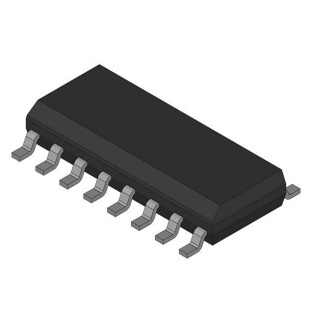
LMX2336L 5.5 mA at 5V. The LMX2335L is available in SO,
TSSOP and CSP 16-pin surface mount plastic packages.
The LMX2336L is available in a TSSOP 20-pin and CSP
24-pin surface mount plastic package.
n Ultra low current consumption
n 2.7V to 5.5V operation
n Selectable synchronous and asynchronous powerdown
mode:
ICC = 1 µA (typ)
n Dual modulus prescaler: 64/65 or 128/129
n Selectable charge pump TRI-STATE ® mode
n Selectable charge pump current levels
n Selectable Fastlock™ mode
n Upgrade and compatible to LMX2335/36
n Small-outline, plastic, surface mount TSSOP package
n LMX2336 available in CSP package
Applications
n Cellular telephone systems (AMPS, ETACS, RCR-27)
n Cordless telephone systems
(DECT, ISM , PHS, CT-1+)
n Personal Communication Systems
(DCS-1800, PCN-1900)
n Dual Mode PCS phones
n Cable TV Tuners (CATV)
n Other wireless communication systems
Functional Block Diagram
01280701
TRI-STATE ® is a registered trademark of National Semiconductor Corporation.
Fastlock™, MICROWIRE™ and PLLatinum™ are trademarks of National Semiconductor Corporation.
© 2004 National Semiconductor Corporation
DS012807
www.national.com
LMX2335L/LMX2336L PLLatinum Low Power Dual Frequency Synthesizer for RF Personal
Communications
PRELIMINARY
�LMX2335L/LMX2336L
Connection Diagrams
LMX2335L
(Top View)
LMX2335L
(Top View)
01280702
Order Number LMX2335LM or LM2335LTM
NS Package Number M16A and MTC16
01280738
Order Number LMX2335LSLB
NS Package Number SLB16A
LMX2336L
(Top View)
LMX2336L
(Top View)
01280703
Order Number LMX2336LTM
NS Package Number MTC20
01280736
Order Number LMX2336LSLB
NS Package Number SLB24A
Pin Descriptions
Pin No.
Pin No.
Pin No.
Pin No.
2336LTM 2336LSLB 2335LTM 2335LSLB
Pin
I/O
Description
Name
1
24
1
16
VCC1
2
2
2
1
Vp1
3
3
3
2
Do1
4
4
4
3
GND
5
5
5
4
fIN 1
I
RF1 prescaler input. Small signal input from the VCO.
6
6
X
X
/fIN 1
I
RF1 prescaler complementary input. A bypass capacitor should
be placed as close as possible to this pin and be connected
directly to the ground plane. Capacitor is optional with loss of
some sensitivity.
7
7
X
X
GND
www.national.com
Power supply voltage input for RF1 analog and RF1 digital
circuits. Input may range from 2.7V to 5.5V. VCC1 must equal
VCC2. Bypass capacitors should be placed as close as possible to
this pin and be connected directly to the ground plane.
Power supply for RF1 charge pump. Must be ≥ VCC.
O
RF1 charge pump output. For connection to a loop filter for driving
the input of an external VCO.
LMX2335L: Ground for RF1 analog and RF1 digital circuits.
LMX2336L: Ground for RF digital circuits.
Ground for RF1 analog circuitry.
2
�Pin No.
Pin No.
(Continued)
Pin No.
Pin No.
2336LTM 2336LSLB 2335LTM 2335LSLB
Pin
I/O
Description
Name
8
8
6
5
OSCin
I
Oscillator input. The input has a VCC/2 input threshold and can be
driven from an external CMOS or TTL logic gate.
9
10
7
6
OSCout
O
Oscillator output.
10
11
8
7
FoLD
O
Multiplexed output of the programmable or reference dividers, lock
detect signals and Fastlock mode. CMOS output (see
Programmable Modes).
11
12
9
8
Clock
I
High impedance CMOS Clock input. Data for the various latches
is clocked in on the rising edge, into the 20-bit shift register.
12
14
10
9
Data
I
Binary serial data input. Data entered MSB first. The last two bits
are the control bits. High impedance CMOS input.
13
15
11
10
LE
I
Load enable high impedance CMOS input. When LE goes HIGH,
data stored in the shift registers is loaded into one of the 4
appropriate latches (control bit dependent).
14
16
X
X
GND
15
17
X
X
/fIN2
I
RF2 prescaler complementary input. A bypass capacitor should
be placed as close as possible to this pin and be connected
directly to the ground plane. Capacitor is optional with loss of
some sensitivity.
16
18
12
11
fIN 2
I
RF2 prescaler input. Small signal input from the VCO.
17
19
13
12
GND
18
20
14
13
Do 2
19
22
15
14
Vp2
Power supply for RF2 charge pump. Must be ≥ VCC.
20
23
16
15
VCC2
Power supply voltage input for RF2 analog, RF2 digital,
MICROWIRE, FoLD and oscillator circuits. Input may range from
2.7V to 5.5V. VCC2 must equal VCC1. Bypass capacitors should
be placed as close as possible to this pin and be connected
directly to the ground plane.
X
1, 9, 13, 21
X
X
NC
No connect.
Ground for RF2 analog circuitry.
LMX2335L: Ground for RF2 analog, RF2 digital, MICROWIRE,
FoLD and Oscillator circuits. LMX2336L: Ground for IF digital,
MICROWIRE, FoLD and oscillator circuits.
O
RF2 charge pump output. For connection to a loop filter for driving
the input of an external VCO.
3
www.national.com
LMX2335L/LMX2336L
Pin Descriptions
�LMX2335L/LMX2336L
Block Diagram
01280704
Note 1: VCC1 supplies power to the RF1 prescaler, N-counter, R-counter, and phase detector. VCC2 supplies power to the RF2 prescaler, N-counter, phase
detector, R-counter along with the OSCin buffer, MICROWIRE, and FoLD. VCC1 and VCC2 are clamped to each other by diodes and must be run at the same
voltage level.
Note 2: VP1 and VP2 can be run separately as long as VP ≥ VCC.
LMX2335L Pin # → 8/10 ← LMX2336L Pin #
Pin Name → FoLD
X signifies a function not bonded out to a pin
www.national.com
4
�Recommended Operating
Conditions
(Notes 1,
2)
If Military/Aerospace specified devices are required,
please contact the National Semiconductor Sales Office/
Distributors for availability and specifications.
Power Supply Voltage
VCC
2.7V to 5.5V
VP
Power Supply Voltage
VCC
−0.3V to +6.5V
VP
−0.3V to +6.5V
Operating Temperature (TA)
−0.3V to VCC
+0.3V
Storage Temperature Range (TS)
−65˚C to +150˚C
Lead Temperature (solder 4 sec.)
(TL)
+260˚C
−40˚C to +85˚C
Note 1: Absolute Maximum Ratings indicate limits beyond which damage to
the device may occur. Recommended Operating Conditions indicate conditions for which the device is intended to be functional, but do not guarantee
specific performance limits. For guaranteed specifications and test conditions, see the Electrical Characteristics. The guaranteed specifications apply
only for the test conditions listed.
Voltage on Any Pin
with GND = 0V (VI)
VCC to +5.5V
Note 2: This device is a high performance RF integrated circuit with an ESD
rating < 2 keV and is ESD sensitive. Handling and assembly of this device
should only be done at ESD protected work stations.
Electrical Characteristics
VCC = 5.0V, VP = 5.0V; TA = 25˚C, except as specified
Symbol
Parameter
Conditions
Value
Min
ICC
Power Supply
LMX2335L
Current
VCC = 2.7V to 5.5V
Units
Typ
Max
4.0
5.2
mA
RF1 and RF2
ICC
LMX2335L RF1 only
2.0
2.6
mA
ICC
LMX2336L
5.5
7
mA
3.3
RF1 and RF2
LMX2336L RF1 only
fIN 1
fIN 2
Operating
Frequency
fIN1
LMX2335L
LMX2336L
fIN2
ICC-PWDN
Powerdown Current
fOSC
Oscillator Frequency
LMX2335L/2336L
fOSC
4.3
mA
0.100
1.1
GHz
0.050
1.1
GHz
0.200
2.0
GHz
0.050
1.1
GHz
10
µA
MHz
VCC = 5.5V
1
With resonator load on OSCout
5
20
No load on OSCout
5
40
MHz
fφ
Maximum Phase Detector Frequency
PfIN
RF Input Sensitivity
VCC = 3.0V, f > 100 MHz
−15
0
VCC = 5.0V, f > 100 MHz
−10
0
VOSC
Oscillator Sensitivity
OSCin
0.5
VPP
VIH
High-Level Input Voltage
(Note 4)
0.8 VCC
V
VIL
Low-Level Input Voltage
(Note 4)
IIH
High-Level Input Current
VIH = VCC = 5.5V (Note 4)
−1.0
−1.0
PfIN
10
IIL
Low-Level Input Current
VIL = 0V, VCC = 5.5V (Note 4)
IIH
Oscillator Input Current
VIH = VCC = 5.5V
IIL
Oscillator Input Current
VIL = 0V, VCC = 5.5V
MHz
dBm
0.2 VCC
V
1.0
µA
1.0
µA
100
µA
−100
µA
IDo-SOURCE Charge Pump Output Current
VDo = VP/2, ICPo = LOW
(Note 3)
−1.25
mA
IDo-SINK
VDo = VP/2, ICPo = LOW
(Note 3)
1.25
mA
IDo-SOURCE
VDo = VP/2, ICPo = HIGH
(Note 3)
−5.00
mA
IDo-SINK
VDo = VP/2, ICPo = HIGH
(Note 3)
5.00
mA
IDo-TRI
Charge Pump
0.5V ≤ VDo ≤ VCC − 0.5V
TRI-STATE Current
T A= 25˚C
5
−5.0
5.0
nA
www.national.com
LMX2335L/LMX2336L
Absolute Maximum Ratings
�LMX2335L/LMX2336L
Electrical Characteristics
(Continued)
VCC = 5.0V, VP = 5.0V; TA = 25˚C, except as specified
Symbol
Parameter
Conditions
Value
Min
Typ
Units
Max
IDo-SINK vs Charge Pump Sink
IDo-SOURCE vs Soure Mismatch
VDo = VP/2
TA = 25˚C
(Note 5)
3
%
IDo vs VDo Charge Pump
Current Vs Voltage
0.5≤ VDO ≤Vp-0.5V
TA = 25˚C
(Note 5)
10
%
IDo vs TA
Charge Pump
Current vs
Temperature
VDo = VP/2
-40˚C≤ TA ≤85˚C
(Note 5)
10
%
VOH
High-Level Output Voltage
IOH = −500 µA
VOL
Low-Level Output Voltage
IOL = 500 µA
tCS
Data to Clock Set Up Time
See Data Input Timing
50
ns
tCH
Data to Clock Hold Time
See Data Input Timing
10
ns
tCWH
Clock Pulse Width High
See Data Input Timing
50
ns
tCWL
Clock Pulse Width Low
See Data Input Timing
50
ns
tES
Clock to Load Enable Set Up Time
See Data Input Timing
50
ns
tEW
Load Enable Pulse Width
See Data Input Timing
50
ns
Note 3: See PROGRAMMABLE MODES for ICPo description.
Note 4: Clock, Data and LE does not include fIN1, fIN2 and OSCin.
Note 5: See Charge Pump Current Specification Definitions below
www.national.com
6
VCC − 0.4
V
0.4
V
�LMX2335L/LMX2336L
Charge Pump Current Specification Definitions
01280718
I1 = CP sink current at VDo = VP − ∆V
I2 = CP sink current at VDo = VP/2
I3 = CP sink current at VDo = ∆V
I4 = CP source current at VDo = VP − ∆V
I5 = CP source current at VDo = VP/2
I6 = CP source current at VDo = ∆V
V = Voltage offset from positive and negative rails. Dependent on VCO tuning range relative to VCC and ground. Typical values are between 0.5V and 1.0V.
1. IDo vs VDo = Charge Pump Output Current magnitude variation vs Voltage =
[1⁄2 * {|I1| − |I3|}]/[1⁄2 * {|I1| + |I3|}] * 100%
and
[1⁄2 * {|I4| − |I6|}]/[1⁄2 * {|I4| + |I6|}] * 100%
2. IDo-sink vs IDo-source = Charge Pump Output Current Sink vs Source Mismatch =
[|I2| − |I5|]/[1⁄2 * {|I2| + |I5|}] * 100%
3. IDo vs TA =
Charge Pump Output Current magnitude variation vs Temperature =
[|I2 @ temp| − |I2 @ 25˚C|]/|I2 @ 25˚C| * 100%
and
[|I5 @ temp| − |I5 @ 25˚C|]/|I5 @ 25˚C| * 100%
RF Sensitivity Test Block Diagram
01280719
Note 6: N = 10,000R = 50P = 64
Note 7: Sensitivity limit is reached when the error of the divided RF output, FoLD, is ≥ 1 Hz.
7
www.national.com
�LMX2335L/LMX2336L
Typical Performance Characteristics
ICC vs VCC
LMX2336L
ICC vs VCC
LMX2335L
01280720
01280721
Charge Pump Current vs Do Voltage
Icp = LOW
Charge Pump Current vs Do Voltage
Icp = HIGH
01280722
www.national.com
01280723
8
�(Continued)
LMX2335L Input Impedance (for SO package)
VCC = 2.7V to 5.5V, fIN = 50 MHz to 1.5 GHz
LMX2336L Input Impedance (for TSSOP package)
VCC = 2.7V to 5.5V, fIN = 50 MHz to 2.5 GHz
01280724
01280725
Marker 1 = 1 GHz, Real = 94, Imaginary = −118
Marker 1 = 1 GHz, Real = 97, Imaginary = −146
Marker 2 = 1.2 GHz, Real = 72, Imaginary = −88
Marker 2 = 1.89 GHz, Real = 43, Imaginary = −67
Marker 3 = 1.5 GHz, Real = 53, Imaginary = −45
Marker 3 = 2.5 GHz, Real = 30, Imaginary = −33
Marker 4 = 500 MHz, Real = 201, Imaginary = −224
Marker 4 = 500 MHz, Real = 189, Imaginary = −233
LMX2335L Input Impedance (for TSSOP package)
VCC = 2.7V to 5.5V, fIN = 50 MHz to 2.5 GHz
01280731
9
www.national.com
LMX2335L/LMX2336L
Typical Performance Characteristics
�LMX2335L/LMX2336L
Typical Performance Characteristics
(Continued)
LMX2335L RF/IF PLL, LMX2336 IF PLL (for CSP)
VCC = 2.7V to 5.5V, fIN = 50 MHz to 1.5 GHz
LMX2336L RF Side (for CSP package)
VCC = 2.7V to 5.5V, fIN = 50 MHz to 2.5 GHz
01280739
01280740
Marker 1 = 100 MHz, 446 −j279 ohm
Marker 1 = 0.5 GHz, 169 −j206 ohm
Marker 2 = 500 MHz, 178 −j210 ohm
Marker 2 = 1.0 GHz, 78 −j133 ohm
Marker 3 = 1500 MHz, 84 −j132 ohm
Marker 3 = 1.5 GHz, 50 −j88 ohm
Marker 4 = 2000 MHz, 54 −j84 ohm
Marker 4 = 2.0. GHz, 38 −j60 ohm
IDO TRI-STATE
vs Do Voltage
LMX2335L RF1 Sensitivity vs Frequency
01280727
01280726
www.national.com
10
�LMX2335L/LMX2336L
Typical Performance Characteristics
(Continued)
LMX2335L RF2 Sensitivity vs Frequency
LMX2336L RF1 Sensitivity vs Frequency
01280728
01280729
LMX2336L RF2 Sensitivity vs Frequency
Oscillator Input Sensitivity vs Frequency
01280730
01280737
11
www.national.com
�LMX2335L/LMX2336L
Functional Description
The simplified block diagram below shows the 22-bit data register, two 15-bit R Counters and two 18-bit N Counters (intermediate
latches are not shown). The data stream is clocked (on the rising edge of Clock) into the DATA register, MSB first. The data stored
in the shift register is loaded into one of the 4 appropriate latches on the rising edge of LE. The last two bits are the Control Bits.
The DATA is transferred into the counters as follows:
Control Bits
DATA Location
C1
C2
0
0
RF2 R Counter
0
1
RF1 R Counter
1
0
RF2 N Counter
1
1
RF1 N Counter
01280705
PROGRAMMABLE REFERENCE DIVIDERS (RF1 AND RF2 R COUNTERS)
If the Control Bits are 00 or 01 (00 for RF2 and 01 for RF1) data is transferred from the 22-bit shift register into a latch which sets
the 15-bit R Counter. Serial data format is shown below.
01280706
15-BIT PROGRAMMABLE REFERENCE DIVIDER RATIO (R COUNTER)
Divide R
R
R
R
R
R
R
R
R
R
R
15 14 13 12 11 10
9
8
7
6
5
4
3
2
1
3
0
0
0
0
0
0
0
0
0
0
0
0
0
1
1
4
0
0
0
0
0
0
0
0
0
0
0
0
1
0
0
•
32767
•
1
•
1
•
1
•
1
•
1
•
1
•
1
•
1
•
1
•
1
•
1
•
1
•
1
•
1
•
1
Ratio
R
R
R
R
Notes:
Divide ratios less than 3 are prohibited.
Divide ratio: 3 to 32767
R1 to R15: These bits select the divide ratio of the programmable reference divider.
Data is shifted in MSB first.
www.national.com
12
�(Continued)
PROGRAMMABLE DIVIDER (N COUNTER)
Each N counter consists of the 7-bit swallow counter (A counter) and the 11-bit programmable counter (B counter). If the Control
Bits are 10 or 11 (10 for RF2 counter and 11 for RF1 counter) data is transferred from the 20-bit shift register into a 7-bit latch
(which sets the Swallow (A) Counter) and an 11-bit latch (which sets the 11-bit programmable (B) Counter), MSB first. Serial data
format is shown below.
01280707
7-BIT SWALLOW COUNTER DIVIDE RATIO (A COUNTER)
Divide
Ratio
N N N N N N N
7 6 5 4 3 2 1
A
0
0
0
0
0
0
0
0
1
0
0
0
0
0
0
1
•
•
•
•
•
•
•
•
127
1
1
1
1
1
1
1
Notes:
Divide ratio: 0 to 127
B≥A
A