OBSOLETE
LMX2377U
www.ti.com
SNAS140E – MAY 2001 – REVISED MARCH 2013
PLLatinum™ Ultra Low Power Dual Frequency Synthesizer for RF Personal
Communications
2.5 GHz/1.2 GHz
Check for Samples: LMX2377U
FEATURES
DESCRIPTION
•
•
•
•
•
The LMX2377U device is a high performance
frequency synthesizer with integrated dual modulus
prescalers. The LMX2377U device is designed for
use as a local oscillator for the first and second RF of
a dual conversion radio transceiver.
1
23
•
•
•
•
•
•
Ultra Low Current Consumption
Upgrade and Compatible to the LMX2370
2.7V to 5.5V Operation
1.8V to 5.0V MICROWIRE Logic Interface
Selectable Synchronous or Asynchronous
Powerdown Mode:
– ICC-PWDN = 1 μA typical
Selectable Dual Modulus Prescaler:
– Main: 16/17 or 32/33
– Aux: 8/9 or 16/17
Selectable Charge Pump TRI-STATE Mode
Programmable Charge Pump Current Levels
– Main and Aux: 0.95 or 3.8 mA
Selectable Fastlock Mode for the Main
Synthesizer
Open Drain Analog Lock Detect Output
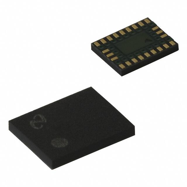
Available in 20-Pin TSSOP, 24-Pin PLGA, and
20-Pin ULGA
APPLICATIONS
•
•
•
•
A 16/17 or a 32/33 prescale ratio can be selected for
the Main synthesizer. An 8/9 or a 16/17 prescale ratio
can be selected for the Aux synthesizer. Using a
proprietary digital phase lock technique, the
LMX2377U device generates very stable, low noise
control signals for UHF and VHF voltage controlled
oscillators. Both the Main and Aux synthesizers
include a two-level programmable charge pump. The
Main synthesizer has dedicated Fastlock circuitry.
Serial data is transferred to the devices via a threewire interface (Data, LE, Clock). The low voltage logic
interface allows connection to 1.8V devices. Supply
voltages from 2.7V to 5.5V are supported. The
LMX2377U features ultra low current consumption,
typically 3.5 mA at 3.0V.
The LMX2377U devices are available in 20-Pin
TSSOP, 24-Pin PLGA, and 20-Pin ULGA surface
mount plastic packages.
Mobile Handsets
– (GSM, GPRS, W-CDMA, CDMA, PCS, AMPS,
PDC, DCS)
Cordless Handsets
– (DECT, DCT)
Wireless Data
Cable TV Tuners
1
2
3
Please be aware that an important notice concerning availability, standard warranty, and use in critical applications of
Texas Instruments semiconductor products and disclaimers thereto appears at the end of this data sheet.
PLLatinum is a trademark of Texas Instruments.
All other trademarks are the property of their respective owners.
PRODUCTION DATA information is current as of publication date.
Products conform to specifications per the terms of the Texas
Instruments standard warranty. Production processing does not
necessarily include testing of all parameters.
Copyright © 2001–2013, Texas Instruments Incorporated
�OBSOLETE
LMX2377U
SNAS140E – MAY 2001 – REVISED MARCH 2013
Figure 1. Thin Shrink Small
Outline Package
www.ti.com
Figure 2. Plastic Land Grid Array
Figure 3. Ultra Thin Land Grid
Array
Functional Block Diagram
2
Submit Documentation Feedback
Copyright © 2001–2013, Texas Instruments Incorporated
Product Folder Links: LMX2377U
�OBSOLETE
LMX2377U
www.ti.com
SNAS140E – MAY 2001 – REVISED MARCH 2013
Connection Diagrams
Top View
Top View
Figure 4. 20-Pin TSSOP
See PW Package
Figure 5. 24-Pin PLGA
See NPH Package
Top View
Figure 6. 20-Pin ULGA
See NPE Package
Submit Documentation Feedback
Copyright © 2001–2013, Texas Instruments Incorporated
Product Folder Links: LMX2377U
3
�OBSOLETE
LMX2377U
SNAS140E – MAY 2001 – REVISED MARCH 2013
www.ti.com
PIN DESCRIPTIONS
Pin
Name
Pin No.
20-Pin ULGA
Pin No.
24-Pin PLGA
Pin No.
20-Pin TSSOP
I/O
Description
VCC
20
24
1
—
Power supply bias for the Main PLL analog and digital circuits. VCC
may range from 2.7V to 5.5V. Bypass capacitors should be placed as
close as possible to this pin and be connected directly to the ground
plane.
VP Main
1
2
2
—
Main PLL charge pump power supply. Must be ≥ VCC.
Do Main
2
3
3
O
Main PLL charge pump output. The output is connected to the
external loop filter, which drives the input of the VCO.
Ground for the Main PLL digital circuitry.
GND
3
4
4
—
fIN Main
4
5
5
I
Main PLL prescaler input. Small signal input from the VCO.
fIN Main
5
6
6
I
Main prescaler complementary input. For single ended operation, this
pin should be AC grounded. The LMX2377U Main PLL can be driven
differentially when the bypass capacitor is omitted.
4
GND
6
7
7
—
OSCin
7
8
8
I
Ground for the Main PLL analog circuitry.
GND
8
10
9
—
Ground for the Aux PLL digital circuitry, MICROWIRE, FoLD, and
oscillator circuits.
FoLD
9
11
10
O
Programmable multiplexed output pin. Functions as a general purpose
CMOS TRI-STATE output, Main/Aux PLL open drain analog lock
detect output, N and R divider output or Fastlock output, which
connects a parallel resistor to the external loop filter.
Clock
10
12
11
I
MICROWIRE Clock input. High impedance CMOS input. Data is
clocked into the 22-bit shift register on the rising edge of Clock.
Data
11
14
12
I
MICROWIRE Data input. High impedance CMOS input. Binary serial
data. The MSB of Data is shifted in first. The last two bits are the
control bits.
LE
12
15
13
I
MICROWIRE Latch Enable input. High impedance CMOS input. When
LE transitions HIGH, Data stored in the shift register is loaded into
one of 4 internal control registers.
Vµc
13
16
14
—
Power supply bias for the MICROWIRE circuitry. Must be ≤ VCC.
Typically connected to the same supply level as the microprocessor or
baseband controller to enable programming at low voltages.
Ground for the Aux PLL analog circuitry.
Reference oscillator input. It has an approximate VCC/2 input threshold
and can be driven from an external CMOS or TTL logic gate.
GND
14
17
15
—
fIN Aux
15
18
16
I
GND
16
19
17
—
Ground for the Aux PLL digital circuitry, MICROWIRE, FoLD, and
oscillator circuits.
Do Aux
17
20
18
O
Aux PLL charge pump output. the output is connected to an external
loop filter, which drives the input of the VCO.
VP Aux
18
22
19
—
Aux PLL charge pump power supply. Must be ≥ VCC.
VCC
19
23
20
—
Power supply bias for the Aux PLL analog and digital circuits, FoLD,
and oscillator circuits. VCC may range from 2.7V to 5.5V. Bypass
capacitors should be placed as close as possible to this pin and be
connected directly to the ground plane.
NC
—
1, 9, 13, 21
—
—
No Connect
Aux PLL prescaler input. Small signal input from the VCO.
Submit Documentation Feedback
Copyright © 2001–2013, Texas Instruments Incorporated
Product Folder Links: LMX2377U
�OBSOLETE
LMX2377U
www.ti.com
SNAS140E – MAY 2001 – REVISED MARCH 2013
Detailed Block Diagram
A.
1. VCC supplies power to the Main and Aux prescalers, Main and Aux feedback dividers, Main and Aux reference
dividers, Main and Aux phase detectors, the OSCin buffer, and FoLD circuitry.
B.
Vμc supplies power to the MICROWIRE circuitry.
C.
VP Main and VP Aux supply power to the charge pumps. They can be run separately as long as VP Main ≥ VCC and
VP Aux ≥ VCC.
Submit Documentation Feedback
Copyright © 2001–2013, Texas Instruments Incorporated
Product Folder Links: LMX2377U
5
�OBSOLETE
LMX2377U
SNAS140E – MAY 2001 – REVISED MARCH 2013
www.ti.com
These devices have limited built-in ESD protection. The leads should be shorted together or the device placed in conductive foam
during storage or handling to prevent electrostatic damage to the MOS gates.
Absolute Maximum Ratings (1) (2) (3) (4)
Power Supply Voltage
VCC to GND
−0.3V to +6.5V
VP Main to GND
−0.3V to +6.5V
VP Aux to GND
−0.3V to +6.5V
−0.3V to VCC+0.3V
Voltage on any pin to GND (VI)
VI must be < +6.5V
−65°C to +150°C
Storage Temperature Range (TS)
Lead Temperature (solder 4 s) (TL)
+260°C
TSSOP θJA Thermal Impedance
114.5°C/W
LGA θJA Thermal Impedance
(1)
(2)
(3)
(4)
112°C/W
This device is a high performance RF integrated circuit with an ESD rating


 工商网监
湘ICP备2023018690号
工商网监
湘ICP备2023018690号
