Product
Folder
Sample &
Buy
Support &
Community
Tools &
Software
Technical
Documents
LMX2541
SNOSB31J – JULY 2009 – REVISED DECEMBER 2014
LMX2541 Ultra-Low Noise PLLatinum Frequency Synthesizer With Integrated VCO
1 Features
3 Description
•
The LMX2541 device is an ultra low-noise frequency
synthesizer which integrates a high-performance
delta-sigma fractional N PLL, a VCO with fully
integrated tank circuit, and an optional frequency
divider. The PLL offers an unprecedented normalized
noise floor of –225 dBc/Hz and can be operated with
up to 104 MHz of phase-detector rate (comparison
frequency) in both integer and fractional modes. The
PLL can also be configured to work with an external
VCO.
1
•
•
•
•
•
•
•
•
•
•
•
•
•
•
•
•
•
•
Multiple Frequency Options Available
(See Device Comparison Table)
Frequencies From 31.6 MHz to 4000 MHz
Very Low RMS Noise and Spurs
–225 dBc/Hz Normalized PLL Phase Noise
Integrated RMS Noise (100 Hz to 20 MHz)
– 2 mRad (100 Hz to 20 MHz) at 2.1 GHz
– 3.5 mRad (100 Hz to 20 MHz) at 3.5 GHz
Ultra Low-Noise Integrated VCO
External VCO Option (Internal VCO Bypassed)
VCO Frequency Divider 1 to 63 (All Values)
Programmable Output Power
Up to 104-MHz Phase Detector Frequency
Integrated Low-Noise LDOs
Programmable Charge Pump Output
Partially Integrated Loop Filter
Digital Frequency Shift Keying (FSK) Modulation
Pin
Integrated Reference Crystal Oscillator Circuit
Hardware and Software Power Down
FastLock Mode and VCO-Based Cycle Slip
Reduction
Analog and Digital Lock Detect
1.6-V Logic Compatibility
The LMX2541 integrates several low-noise, highprecision LDOs and output driver matching network to
provide higher supply noise immunity and more
consistent performance, while reducing the number of
external components. When combined with a highquality reference oscillator, the LMX2541 generates a
very stable, ultra low-noise signal.
The LMX2541 is offered in a family of 6 devices with
varying VCO frequency range from 1990 MHz up to 4
GHz. Using a flexible divider, the LMX2541 can
generate frequencies as low as 31.6 MHz.
The LMX2541 is a monolithic integrated circuit,
fabricated in a proprietary BiCMOS process. Device
programming is facilitated using a three-wire
MICROWIRE interface that can operate down to 1.6
volts. Supply voltage ranges from 3.15 V to 3.45 V.
The LMX2541 is available in a 36-pin 6-mm × 6-mm
× 0.8-mm WQFN package.
Device Information(1)
2
•
•
•
•
•
Applications
PART NUMBER
Wireless Infrastructure (UMTS, LTE, WiMax)
Broadband Wireless
Wireless Meter Reading
Test and Measurement
FM Mobile Radio
space
PACKAGE
VCO FREQUENCY
(MHz)
LMX2541SQ2060E
WQFN (36)
1990 - 2240
LMX2541SQ2380E
WQFN (36)
2200 - 2530
LMX2541SQ2690E
WQFN (36)
2490 - 2865
LMX2541SQ3030E
WQFN (36)
2810 - 3230
LMX2541SQ3320E
WQFN (36)
3130 - 3600
LMX2541SQ3740E
WQFN (36)
3480 - 4000
(1) For all available packages, see the orderable addendum at
the end of the data sheet.
System Block Diagram
Clean
Reference
Clock
Dist.
Dirty Input
Clock
PLL
Ultra-Clean
Local Oscillator
PLL
LMK04000
LMX2541
(Clock Jitter Cleaner)
(RF Synthesizer)
1
An IMPORTANT NOTICE at the end of this data sheet addresses availability, warranty, changes, use in safety-critical applications,
intellectual property matters and other important disclaimers. PRODUCTION DATA.
�LMX2541
SNOSB31J – JULY 2009 – REVISED DECEMBER 2014
www.ti.com
Table of Contents
1
2
3
4
5
6
7
Features ..................................................................
Applications ...........................................................
Description .............................................................
Revision History.....................................................
Device Comparison Table.....................................
Pin Configuration and Functions .........................
Specifications.........................................................
7.1
7.2
7.3
7.4
7.5
7.6
7.7
1
1
1
2
3
4
6
Absolute Maximum Ratings ...................................... 6
ESD Ratings.............................................................. 6
Recommended Operating Conditions....................... 6
Thermal Information .................................................. 6
Electrical Characteristics........................................... 7
Timing Requirements .............................................. 11
Typical Characteristics ............................................ 12
8
Parameter Measurement Information ................ 23
9
Detailed Description ............................................ 25
8.1 Bench Test Setups.................................................. 23
9.1 Overview ................................................................. 25
9.2
9.3
9.4
9.5
9.6
Functional Block Diagrams .....................................
Feature Description.................................................
Device Functional Modes........................................
Programming...........................................................
Register Maps .........................................................
25
26
36
37
38
10 Application and Implementation........................ 51
10.1 Application Information.......................................... 51
10.2 Typical Application ............................................... 59
11 Power Supply Recommendations ..................... 61
12 Layout................................................................... 62
12.1 Layout Guidelines ................................................. 62
12.2 Layout Example .................................................... 63
13 Device and Documentation Support ................. 64
13.1
13.2
13.3
13.4
Device Support......................................................
Trademarks ...........................................................
Electrostatic Discharge Caution ............................
Glossary ................................................................
64
64
64
64
14 Mechanical, Packaging, and Orderable
Information ........................................................... 64
4 Revision History
Changes from Revision I (February 2013) to Revision J
•
Added ESD Ratings table, Feature Description section, Device Functional Modes, Application and Implementation
section, Power Supply Recommendations section, Layout section, Device and Documentation Support section, and
Mechanical, Packaging, and Orderable Information section .................................................................................................. 1
Changes from Revision H (February 2013) to Revision I
•
2
Page
Page
Changed layout of National Data Sheet to TI format ........................................................................................................... 36
Submit Documentation Feedback
Copyright © 2009–2014, Texas Instruments Incorporated
Product Folder Links: LMX2541
�LMX2541
www.ti.com
SNOSB31J – JULY 2009 – REVISED DECEMBER 2014
5 Device Comparison Table
VCO
_DIV
LMX2541SQ2060E
LMX2541SQ2380E
LMX2541SQ2690E
LMX2541SQ3030E
LMX2541SQ3320E
LMX2541SQ3740E
Fmin
Fmax
Fmin
Fmax
Fmin
Fmax
Fmin
Fmax
Fmin
Fmax
Fmin
Fmax
1
1990.0
2240.0
2200.0
2530.0
2490.0
2865.0
2810.0
3230.0
3130.0
3600.0
3480.0
4000.0
2
995.0
1120.0
1100.0
1265.0
1245.0
1432.5
1405.0
1615.0
1565.0
1800.0
1740.0
2000.0
3
663.3
746.7
733.3
843.3
830.0
955.0
936.7
1076.7
1043.3
1200.0
1160.0
1333.3
4
497.5
560.0
550.0
632.5
622.5
716.3
702.5
807.5
782.5
900.0
870.0
1000.0
5
398.0
448.0
440.0
506.0
498.0
573.0
562.0
646.0
626.0
720.0
696.0
800.0
6
331.7
373.3
366.7
421.7
415.0
477.5
468.3
538.3
521.7
600.0
580.0
666.7
7
284.3
320.0
314.3
361.4
355.7
409.3
401.4
461.4
447.1
514.3
497.1
571.4
8
248.8
280.0
275.0
316.3
311.3
358.1
351.3
403.8
391.3
450.0
435.0
500.0
...
...
...
...
...
...
...
...
...
...
...
...
...
63
31.6
35.6
34.9
40.2
39.5
45.5
44.6
51.3
49.7
57.1
55.2
63.5
All devices have continuous frequency coverage below a divide value of 8 (7 for most devices) down to their
minimum frequency achievable with divide by 63. The numbers in bold show the upper end of this minimum
continuous frequency range. For instance, the LMX2541SQ3740E option offers continuous frequency coverage
from 55.2 MHz to 571.4 MHz and LMX2541SQ2060E offers continuous frequency coverage from 31.6 MHz to
280 MHz. If using the part in External VCO mode, all parts have roughly the same performance and any option
will do.
Submit Documentation Feedback
Copyright © 2009–2014, Texas Instruments Incorporated
Product Folder Links: LMX2541
3
�LMX2541
SNOSB31J – JULY 2009 – REVISED DECEMBER 2014
www.ti.com
6 Pin Configuration and Functions
RFout
NC
LE
CLK
DATA
VccDiv
Bypass
VccBias
VccDig
NJK Package
36-Pin WQFN
Top View
36
35
34
33
32
31
30
29
28
GND
1
27
GND
VregRFout
2
26
VregFRAC
VccRFout
3
25
VccFRAC
L1
4
24
RFoutEN
23
VccOSCin
0
GND
21
OSCin
VregVCO
8
20
Ftest/LD
VrefVCO
9
19
VccPLL2
11
12
13
14
15
16
17
18
VccCP2
10
FLout
7
CPout
VccVCO
Vtune
OSCin*
VccCP1
22
VccPLL1
6
ExtVCOin
L2
CE
5
GND
Lmid
Pin Functions
PIN
4
TYPE
DESCRIPTION
NAME
NO.
Bypass
30
Bypass
Put a cap to the VccBias pin.
CE
11
CMOS
Chip Enable.
The device needs to be programmed for this pin to properly power down the device.
CLK
33
High-Z Input
CPout
16
Output
DATA
32
High-Z Input
MICROWIRE serial data input. High impedance CMOS input.
ExtVCOin
12
RF Input
Optional input for use with an external VCO.
This pin should be AC coupled if used or left open if not used.
FLout
17
Output
Fastlock output.
Ftest/LD
20
Output
Software controllable multiplexed CMOS output.
Can be used to monitor PLL lock condition.
GND
0
GND
GND
1
GND
GND
10
GND
GND
27
GND
L1
4
NC
Do not connect this pin.
L2
6
NC
Do not connect this pin.
LE
34
High-Z Input
Lmid
5
NC
Do not connect this pin.
NC
35
NC
No connect.
OSCin
21
High-Z Input
MICROWIRE clock input. High impedance CMOS input.
This pin is used for the digital FSK modulation feature.
Charge pump output.
The DAP pad must be grounded.
MICROWIRE Latch Enable input. High impedance CMOS input.
Oscillator input signal. If not being used with an external crystal, this input should be AC
coupled.
Submit Documentation Feedback
Copyright © 2009–2014, Texas Instruments Incorporated
Product Folder Links: LMX2541
�LMX2541
www.ti.com
SNOSB31J – JULY 2009 – REVISED DECEMBER 2014
Pin Functions (continued)
PIN
TYPE
DESCRIPTION
NAME
NO.
OSCin*
22
High-Z Input
RFout
36
RF Output
RFoutEN
24
Input
VccBias
29
Supply
Supply for Bias circuitry that is for the whole chip.
VccCP1
14
Supply
Power supply for PLL charge pump.
VccCP2
18
Supply
Power supply for PLL charge pump.
VccDig
28
Supply
Supply for digital circuitry, such the MICROWIRE.
VccDiv
31
Supply
Supply for the output divider
VccFRAC
25
Supply
(LDO Input)
VccOSCin
23
Supply
Supply for the OSCin buffer.
VccPLL1
13
Supply
Power supply for PLL.
VccPLL2
19
Supply
Power supply for PLL.
VccRFout
3
Supply
(LDO Input)
Supply for the RF output buffer.
VccVCO
7
Supply
(LDO Input)
Supply for the VCO.
VregFRAC
26
LDO Output
Regulated power supply used for the fractional delta-sigma circuitry.
VregRFout
2
LDO Output
LDO Output for RF output buffer.
Complementary oscillator input signal. Can also be used with an external crystal. If not
being used with an external crystal, this input should be AC coupled.
RF output. Must be AC coupled if used.
Software programmable output enable pin.
Power Supply for the PLL fractional circuitry.
VrefVCO
9
LDO Bypass
LDO Bypass
VregVCO
8
LDO Output
LDO Output for VCO
Vtune
15
High-Z Input
Tuning voltage input to the VCO.
Submit Documentation Feedback
Copyright © 2009–2014, Texas Instruments Incorporated
Product Folder Links: LMX2541
5
�LMX2541
SNOSB31J – JULY 2009 – REVISED DECEMBER 2014
www.ti.com
7 Specifications
7.1 Absolute Maximum Ratings
over operating free-air temperature range (unless otherwise noted)
(1) (2)
MIN
MAX
UNIT
Vcc
Power Supply Voltage
–0.3
3.6
V
VIN
Input Voltage to pins other than Vcc Pins
–0.3
(Vcc + 0.3)
V
TL
Lead Temperature (solder 4 sec.)
260
°C
Tstg
Storage Temperature
150
°C
(1)
(2)
(3)
(3)
–65
Stresses beyond those listed under Absolute Maximum Ratings may cause permanent damage to the device. These are stress ratings
only, which do not imply functional operation of the device at these or any other conditions beyond those indicated under Recommended
Operating Conditions. Exposure to absolute-maximum-rated conditions for extended periods may affect device reliability.
If Military/Aerospace specified devices are required, please contact the Texas Instruments Sales Office/Distributors for availability and
specifications.
Never to exceed 3.6 V.
7.2 ESD Ratings
VALUE
V(ESD)
(1)
(2)
Electrostatic discharge
Human body model (HBM), per ANSI/ESDA/JEDEC JS-001 (1)
±2500
Charged-device model (CDM), per JEDEC specification JESD22C101 (2)
±1750
Machine model (MM)
±400
UNIT
V
JEDEC document JEP155 states that 500-V HBM allows safe manufacturing with a standard ESD control process.
JEDEC document JEP157 states that 250-V CDM allows safe manufacturing with a standard ESD control process.
7.3 Recommended Operating Conditions
MIN
NOM
MAX
Vcc
Power Supply Voltage (All Vcc Pins)
3.15
3.3
3.45
UNIT
V
TA
Ambient Temperature
–40
85
°C
7.4 Thermal Information
THERMAL METRIC
(1)
LMX2541
SQ2060E
LMX2541
SQ2060E
LMX2541
SQ2060E
9 Thermal
Vias (2)
13 Thermal
Vias (3)
16 Thermal
Vias (4)
RθJA
Junction-to-ambient thermal resistance
31.7
30.3
29.8
ψJT
Junction-to-top characterization parameter
7.3
7.3
7.3
(1)
(2)
(3)
(4)
6
UNIT
°C/W
For more information about traditional and new thermal metrics, see the IC Package Thermal Metrics application report, SPRA953.
Recommended for Most Reliable Solderability.
Compromise Between Solderability, Heat Dissipation, and Fractional Spurs.
Recommended for Optimal Heat Dissipation and Fractional Spurs.
Submit Documentation Feedback
Copyright © 2009–2014, Texas Instruments Incorporated
Product Folder Links: LMX2541
�LMX2541
www.ti.com
SNOSB31J – JULY 2009 – REVISED DECEMBER 2014
7.5 Electrical Characteristics
(3.15 V ≤ VCC ≤ 3.45 V, -40°C ≤ TA ≤ 85 °C; except as specified. Typical values are at Vcc = 3.3 V, 25 C.)
PARAMETER
TEST CONDITIONS
MIN
TYP
MAX
VCO_DIV>1
170
204
VCO_DIV=1
130
156
UNIT
CURRENT CONSUMPTION
Default Power
Mode
ICC
Entire Chip Supply Current with
all blocks enabled
IPLL
Current for External VCO Mode
RFoutEN = LOW
72
94
mA
IDIV
Current for Divider Only Mode
VCO_DIV >1
Default Power Mode
84
110
mA
ICCPD
Power Down Current
CE = 0 V, Device Initialized
100
250
µA
300
µA
(1)
(1)
mA
OSCILLATOR (NORMAL MODE OPERATION WITH XO=0)
IIHOSC
in
Oscillator Input High Current for
OSCin and OSCin*
VIH = 2.75 V
IILOSCi
n
Oscillator Input Low Current for
OSCin and OSCin* pins
VIL = 0
–100
OSC_2X = 1
fOSCin
OSCin Frequency Range
(2)
dvOSCin
Slew Rate
vOSCin
Oscillator Sensitivity
OSC_2X = 0
µA
5
52
MODE = 0
5
700
MODE = 1
5
900
(2)
MHz
150
dvOSCin ≥ 150 V/µs
V/µs
Single-Ended
0.2
2.0
Differential
0.4
3.1
5
20
MHz
100
Ω
Vpp
OSCILLATOR (CRYSTAL MODE WITH XO=1)
fXTAL
Crystal Frequency Range
VIH = 2.75 V
ESRXTA Crystal Equivalent Series
Resistance
L
This a requirement for the crystal, not a
characteristic of the LMX2541.
PXTAL
Power Dissipation in Crystal
This requirement is for the crystal, not a
characteristic of the LMX2541.
COSCin
Input Capacitance of OSCin
200
µW
6
pF
PLL
fPD
Phase Detector Frequency
ICPout
Charge Pump
Output Current Magnitude
104
CPG = 1X
100
CPG = 2X
200
CPG = 3X
300
...
µA
...
CPG=32X
ICPoutTR
CP TRI-STATE Current
I
0.4 V < VCPout < Vcc - 0.4
ICPoutM
M
Charge Pump
Sink vs. Source Mismatch
ICPoutV
3200
1
5
VCPout = Vcc / 2
TA = 25°C
3%
10%
Charge Pump
Current vs. CP Voltage Variation
0.4 V < VCPout < Vcc - 0.4
TA = 25°C
4%
ICPoutT
CP Current vs. Temperature
Variation
VCPout = Vcc / 2
8%
Normalized PLL 1/f Noise
LNPLL_flicker(10 kHz)
CPG = 1X
LN(f)
CPG = 32X
–124.5
Normalized PLL Noise Floor
LNPLL_flat(1 Hz)
CPG = 1X
–220.8
CPG = 32X
–225.4
(3)
(1)
(2)
(3)
MHz
–116
nA
dBc/Hz
dBc/Hz
The LMX2541 RFout power level is programmable with the program words of VCOGAIN, OUTTERM, and DIVGAIN. Changing these
words can change the output power of the VCO as well as the current consumption of the output buffer. For the purpose of consistency
in electrical specifications, "Default Power Mode" is defined to be the settings of VCOGAIN = OUTTERM = DIVGAIN = 12.
Not tested in production. Specified by characterization. OSCin is tested only to 400 MHz.
See Application and Implementation for more details on these parameters.
Submit Documentation Feedback
Copyright © 2009–2014, Texas Instruments Incorporated
Product Folder Links: LMX2541
7
�LMX2541
SNOSB31J – JULY 2009 – REVISED DECEMBER 2014
www.ti.com
Electrical Characteristics (continued)
(3.15 V ≤ VCC ≤ 3.45 V, -40°C ≤ TA ≤ 85 °C; except as specified. Typical values are at Vcc = 3.3 V, 25 C.)
PARAMETER
fExtVCOin PLL Input Frequency
pExtVCOi
n
PLL Input Sensitivity
( (2) applies to Max Limit Only)
TEST CONDITIONS
MIN
TYP
MAX
RFout Buffer Enabled and VCO_DIV > 1
400
4000
RFout Buffer Disabled and VCO_DIV = 1
400
6000
fExtVCOin ≤ 4 GHz
–15
10
fExtVCOin > 4 GHz
–5
10
2060E
1990
2240
2380E
2200
2530
2690E
2490
2865
3030E
2810
3230
3320E
3130
3600
3740E
3480
4000
UNIT
MHz
dBm
VCO SPECIFICATIONS
fVCO
Internal VCO Frequency Range
Maximum Allowable Temperature
Drift for Continuous Lock
ΔTCL
pRFout
RF Output Power
ΔPRFout
Change in Output Power
KVtune
Fine Tuning Sensitivity
HSRFout
DERFout
Second Harmonic
(5)
Duty Cycle Error
(5)
PSHVCO VCO Frequency Pushing
PULVCO VCO Frequency Pulling
(4)
(5)
8
Mode = Full Chip Mode
This is the frequency before the
VCO divider.
(2) (4)
,
125
Maximum Frequency
Default Power Mode
VCO_DIV=1
°C
2060E
3.5
2380E
2.8
2690E
1.6
3030E
1.2
3320E
0.2
3740E
–0.3
Fixed Temperature with 100 MHz frequency change
at the output
0.3
Fixed frequency with a change over the entire
temperature range
0.4
The lower number in the range
applies when the VCO is at its
lowest frequency and the higher
number applies when the VCO
is at its highest frequency. A
linear approximation can be
used for frequencies between
these two cases.
2060E
13 - 23
2380E
16 - 30
2690E
17 - 32
3030E
20 - 37
3320E
21 - 37
3740E
24 - 42
VCO_DIV = 2
–20
50 Ω Load
VCO_DIV = 3
–20
Default Power Mode
VCO_DIV = 2
3%
50 Ω Load
VCO_DIV = 3
3%
VCO_DIV = 1
±800
VCO_DIV > 1
±60
(1)
CVregVCO = 4.7 µF, Open Loop
VSWR 1.7 to 1
(6 dB Pad)
dBm
dB
Default Power Mode
(1)
MHz
600
MHz/V
dBc
kHz/V
kHz
Maximum Allowable Temperature Drift for Continuous Lock is how far the temperature can drift in either direction from the value it was
at the time that the R0 register was last programmed, and still have the device stay in lock. The action of programming the R0 register,
even to the same value, activates a frequency calibration routine. This implies that the device will work over the entire frequency range,
but if the temperature drifts more than the maximum allowable drift for continuous lock, then it will be necessary to reload the R0 register
to ensure that it stays in lock. Regardless of what temperature the device was initially programmed at, the temperature can never drift
outside the frequency range of -40°C ≤TA≤ 85°C without violating specifications.
The duty cycle error (DE) and second harmonic (HS) are theoretically related by the equation HS = 10·log| 2π·DE | - 6 dB. A square
wave with 3% duty cycle theoretically has a second harmonic of -20 dBc.
Submit Documentation Feedback
Copyright © 2009–2014, Texas Instruments Incorporated
Product Folder Links: LMX2541
�LMX2541
www.ti.com
SNOSB31J – JULY 2009 – REVISED DECEMBER 2014
Electrical Characteristics (continued)
(3.15 V ≤ VCC ≤ 3.45 V, -40°C ≤ TA ≤ 85 °C; except as specified. Typical values are at Vcc = 3.3 V, 25 C.)
PARAMETER
σΦ
RMS Phase Error
TEST CONDITIONS
Integration Bandwidth
= 100 Hz to 20 MHz
Middle VCO Frequency
100 MHz Wenzel Crystal
Reference
Integer Mode
Optimized Loop Bandwidth
MIN
TYP
2060E
1.6
2380E
1.8
2690E
2.1
3030E
2.1
3320E
2.3
3740E
2.6
MAX
UNIT
mRad
VCO PHASE NOISE (6)
fRFout =
Min VCO
Frequency
L(f)Fout
Phase Noise
2060E
fRFout =
Max VCO
Frequency
fRFout =
Min VCO
Frequency
L(f)Fout
Phase Noise
2380E
fRFout =
Max VCO
Frequency
fRFout =
Min VCO
Frequency
L(f)Fout
Phase Noise
2690E
fRFout =
Max VCO
Frequency
(6)
10-kHz Offset
–89.7
100-kHz Offset
–113.7
1-MHz Offset
–134.9
10-MHz Offset
–155.4
20-MHz Offset
–160.3
10-kHz Offset
–86.5
100-kHz Offset
–111.4
1-MHz Offset
–132.8
10-MHz Offset
–153.4
20-MHz Offset
–158.5
10-kHz Offset
–87.9
100-kHz Offset
–112.7
1-MHz Offset
–133.8
10-MHz Offset
–154.2
20-MHz Offset
–159.5
10-kHz Offset
–83.4
100-kHz Offset
–109.1
1-MHz Offset
–130.8
10-MHz Offset
–151.8
20-MHz Offset
–157.5
10-kHz Offset
–86.9
100-kHz Offset
–111.8
1-MHz Offset
–133.3
10-MHz Offset
–154.2
20-MHz Offset
–159.4
10-kHz Offset
–82.3
100-kHz Offset
–108.4
1-MHz Offset
–130.3
10-MHz Offset
–151.1
20-MHz Offset
–156.7
dBc/Hz
dBc/Hz
dBc/Hz
The VCO phase noise is measured assuming that the loop bandwidth is sufficiently narrow that the VCO noise dominates. The phase
noise is measured with AC_TEMP_COMP = 5 and the device is reloaded at each test frequency. The typical performance
characteristics section shows how the VCO phase noise varies over temperature and frequency.
Submit Documentation Feedback
Copyright © 2009–2014, Texas Instruments Incorporated
Product Folder Links: LMX2541
9
�LMX2541
SNOSB31J – JULY 2009 – REVISED DECEMBER 2014
www.ti.com
Electrical Characteristics (continued)
(3.15 V ≤ VCC ≤ 3.45 V, -40°C ≤ TA ≤ 85 °C; except as specified. Typical values are at Vcc = 3.3 V, 25 C.)
PARAMETER
TEST CONDITIONS
fRFout =
Min VCO
Frequency
L(f)Fout
Phase Noise
3030E
fRFout =
Max VCO
Frequency
fRFout =
Min VCO
Frequency
L(f)Fout
Phase Noise
3320E
fRFout =
Max VCO
Frequency
fRFout =
Min VCO
Frequency
L(f)Fout
Phase Noise
3740E
fRFout =
Max VCO
Frequency
MIN
TYP
10-kHz Offset
–86.1
100-kHz Offset
–110.5
1-MHz Offset
–132.0
10-MHz Offset
–152.2
20-MHz Offset
–157.1
10-kHz Offset
–82.2
100-kHz Offset
–107.7
1-MHz Offset
–129.4
10-MHz Offset
–150.5
20-MHz Offset
–156.1
10-kHz Offset
–84.1
100-kHz Offset
–109.1
1-MHz Offset
–130.7
10-MHz Offset
–151.6
20-MHz Offset
–156.9
10-kHz Offset
–82.0
100-kHz Offset
–107.0
1-MHz Offset
–128.5
10-MHz Offset
–149.6
20-MHz Offset
–155.2
10-kHz Offset
–83.9
100-kHz Offset
–108.3
1-MHz Offset
–129.9
10-MHz offset
–150.6
20-MHz Offset
–156.5
10-kHz Offset
–81.6
100-kHz Offset
–106.5
1-MHz Offset
–127.7
10-MHz Offset
–148.6
20-MHz Offset
–154.2
MAX
UNIT
dBc/Hz
dBc/Hz
dBc/Hz
DIGITAL INTERFACE (DATA, CLK, LE, CE, Ftest/LD, FLout,RFoutEN)
VIH
High-Level Input Voltage
VIL
Low-Level Input Voltage
IIH
High-Level Input Current
VIH = 1.75, XO = 0
IIL
Low-Level Input Current
VIL = 0 V , XO = 0
VOH
High-Level Output Voltage
IOH = 500 µA
VOL
Low-Level Output Voltage
IOL = -500 µA
ILeak
Leakage Current
Ftest/LD and FLout Pins Only
10
1.6
Submit Documentation Feedback
Vcc
V
0.4
V
–5
5
µA
–5
5
µA
2
V
0
–5
0.4
V
5
µA
Copyright © 2009–2014, Texas Instruments Incorporated
Product Folder Links: LMX2541
�LMX2541
www.ti.com
SNOSB31J – JULY 2009 – REVISED DECEMBER 2014
7.6 Timing Requirements
MIN
NOM
MAX
UNIT
tCE
Clock to Enable Low Time
See Figure 1
25
ns
tCS
Data to Clock Set Up Time
See Figure 1
25
ns
tCH
Data to Clock Hold Time
See Figure 1
20
ns
tCWH
Clock Pulse Width High
See Figure 1
25
ns
tCWL
Clock Pulse Width Low
See Figure 1
25
ns
tCES
Enable to Clock Set Up Time
See Figure 1
25
ns
tEWH
Enable Pulse Width High
See Figure 1
25
ns
MSB
DATA
D19
LSB
D18
D17
D16
D15
D0
C3
C2
C1
C0
CLK
tCES
tCS
tCH
tCWH
tCWL
tES
LE
tEWH
Figure 1. Serial Data Timing Diagram
Submit Documentation Feedback
Copyright © 2009–2014, Texas Instruments Incorporated
Product Folder Links: LMX2541
11
�LMX2541
SNOSB31J – JULY 2009 – REVISED DECEMBER 2014
www.ti.com
7.7 Typical Characteristics
PLL NORMALIZED NOISE FLOOR (dBc/Hz)
PLL NORMALIZED NOISE FLOOR (dBc/Hz)
7.7.1 Not Ensured Characteristics
-206
-210
-214
-218
-222
-226
1
10
10
2
3
10
10
4
-216
-218
-220
-222
-224
-226
1X
2X
SLEW RATE (V/Ps)
-105
16X
32X
-115
PLL NORMALIZED 1/f NOISE (dBc/Hz)
PLL NORMALIZED 1/f NOISE (dBc/Hz)
8X
Figure 3. PLL Normalized Noise Floor vs Charge Pump
Gain (Slew Rate = 2000 V/μs)
Figure 2. PLL Normalized Noise Floor vs OSCin Slew Rate
(KPD = 32X)
-109
-113
-117
-121
-125
1
10
4X
CHARGE PUMP GAIN
-117
-119
-121
-123
-125
10
2
10
3
4
1X
10
2X
4X
8X
16X
32X
SLEW RATE (V/Ps)
CHARGE PUMP GAIN
Figure 4. PLL Normalized 1/f Noise vs OSCin Slew Rate
(KPD = 32X)
Figure 5. PLL Normalized 1/f Noise vs Charge Pump Gain
(Slew Rate = 2000 V/μs)
-90
Modeled Noise
Measured Noise
1/f Noise
Flat Noise
-93
Phase Noise (dBc/Hz)
-96
-99
-102
-105
-108
-111
-114
-117
-120
1x10²
1x10³
1x10⁴
Offset (Hz)
1x10⁵
1x10⁶
D001
See Phase Noise Measurement Test Setup
Figure 6. PLL 1/f and Noise Floor Measurement of the LMX2541SQ3740E
12
Submit Documentation Feedback
Copyright © 2009–2014, Texas Instruments Incorporated
Product Folder Links: LMX2541
�LMX2541
www.ti.com
SNOSB31J – JULY 2009 – REVISED DECEMBER 2014
Not Ensured Characteristics (continued)
-80
-145
-88
-147.5
Phase Noise (dBc/Hz)
Phase Noise (dBc/Hz)
-96
-104
-112
-120
-128
-136
-150
-152.5
-155
-157.5
-144
-160
-152
-160
1x10³
1x10⁴
1x10⁵ 1x10⁶
Offset (Hz)
1x10⁷
-162.5
5x101
1x10⁸
1x10²
D001
Engaging the divider reduces the phase noise by 20 ×
log(VCO_DIV) except at far offsets where it adds noise.
Figure 7. Divider Noise Floor vs Divider Value (fVCO = 3700
MHz, Various Values for VCO_DIV)
2x10²
5x10²
Offset (Hz)
1x10³
2x10³
D001
The above plot shows how this noise floor changes as a function of
the frequency of the RFout pin.
Figure 8. Divider Noise Floor vs Frequency
Table 1. Relative VCO Phase Noise Over Temperature Drift
(AC_TEMP_COMP = 24, Vcc = 3.3 V) (1)
TEMPERATURE
(1)
PHASE NOISE CHANGE IN CELSIUS FOR VARIOUS OFFSETS
LOCK
CURRENT
10 kHz
100 kHz
1 MHz
10 MHz
20 MHz
–40
–40
+0.4
–2.0
–1.6
–1.8
–1.6
–40
25
+0.3
+0.5
+0.5
+0.5
+0.4
–40
85
+0.9
+2.0
+2.4
+2.5
+2.3
25
–40
+0.2
–2.2
–1.7
–2.0
–1.8
25
25
This is the default condition to which these other numbers are normalized to.
25
85
+0.6
+1.5
+2.0
+2.0
+1.9
85
–40
+0.2
–2.2
–1.7
–1.9
–1.8
85
25
+0.2
+0.2
+0.3
+0.2
+0.2
85
85
+0.6
+1.8
+2.2
+2.3
+2.1
The table shows the typical degradation for VCO phase noise when the VCO is locked at one temperature and the temperature is
allowed to drift to another temperature. A negative value indicates a phase noise improvement.
Submit Documentation Feedback
Copyright © 2009–2014, Texas Instruments Incorporated
Product Folder Links: LMX2541
13
�LMX2541
SNOSB31J – JULY 2009 – REVISED DECEMBER 2014
www.ti.com
7.7.2 Output Power in Bypass Mode
The following plots show the trends in output power as a function of temperature, voltage, and frequency. For
states where VCOGAIN and OUTTERM are not 12, the table below shows how the output power is modified
based on these programmable settings. The measurement of the output power is sensitive to the test circuit. All
the numbers in the electrical specifications and typical performance curves were obtained from a characterization
setup that accommodate temperature testing and changing of parts. In a more optimized setup the measured RF
output power is typically on the order of 1.5 to 2.4 dB higher.
6
5
OUTTERM=12
4
Vcc = 3.3V
OUTTERM=15
2
POWER (dBm)
POWER (dBm)
3
Vcc = 3.45V
2
1
0
-2
OUTTERM=9
OUTTERM=6
-6
Vcc = 3.15V
-1
OUTTERM=3
-2
1750
2250
2750
3250
3750
-10
1750
4250
2250
Figure 9. Output Power vs Voltage (VCO_DIV = 1,
VCOGAIN = 12, OUTTERM = 12, TA = 25°C)
3750
4250
6
TA = 25o C
4
VCOGAIN=12
TA = -40o C
VCOGAIN=15
2
POWER (dBm)
3
POWER (dBm)
3250
Figure 10. Output Power vs OUTTERM and FREQUENCY
(VCO_DIV = 1, TA = 25 °C, Vcc = 3.3 V, VCOGAIN = 12)
5
2
1
TA = 85o C
0
VCOGAIN=9
-2
VCOGAIN=6
-6
VCOGAIN=3
-1
-2
1750
2750
FREQUENCY (MHz)
FREQUENCY (MHz)
2250
2750
3250
3750
-10
1750
4250
FREQUENCY (MHz)
2250
2750
3250
3750
4250
FREQUENCY (MHz)
Figure 11. Output Power vs Temperature (VCO_DIV = 1,
VCOGAIN = 12, OUTTERM = 12, Vcc = 3.3 V)
Figure 12. Output Power vs VCOGAIN and FREQUENCY
(VCO_DIV = 1, TA = 25 °C, Vcc = 3.3 V, OUTTERM = 12)
Table 2. Change in Output Power in Bypass Mode as a Function of VCOGAIN and OUTTERM
VCOGAIN
OUTTERM
14
3
6
9
12
15
3
–9.7
–8.4
–7.9
–7.8
–7.9
6
–6.6
–4.5
–3.6
–3.4
–3.6
9
–5.7
–3.1
–1.7
–1.3
–1.3
12
–5.4
–2.5
–0.8
+0.0
+0.1
15
–5.3
–2.2
–0.3
+0.8
+1.1
Submit Documentation Feedback
Copyright © 2009–2014, Texas Instruments Incorporated
Product Folder Links: LMX2541
�LMX2541
www.ti.com
SNOSB31J – JULY 2009 – REVISED DECEMBER 2014
7.7.3 Output Power in Divided Mode
The measurement of the output power is sensitive to the test circuit. All the numbers in the electrical
specifications and typical performance curves were obtained from a characterization setup that accommodate
temperature testing and changing of parts. In a more optimized setup the measured RF output power is typically
on the order of 1.5 to 2.4 dB higher.
10
9
Vcc = 3.3 V
8
6
4
Vcc = 3.45 V
POWER (dBm)
POWER (dBm)
OUTTERM=12
6
7
5
4
3
2
1
OUTTERM=6
2
0
OUTTERM=9
-2
-4
-6
Vcc = 3.15 V
OUTTERM=3
-8
0
-1
OUTTERM=15
8
0
500
1000
1500
-10
2500
2000
0
500
Figure 13. Output Power vs Voltage (VCO_DIV > 1,
DIVGAIN = 12, OUTTERM = 12, TA = 25°C)
9
10
8
7
6
POWER (dBm)
POWER (dBm)
4
TA = 25o C
3
2
1
0
500
1000
2500
DIVGAIN=15
DIVGAIN=12
2
0
DIVGAIN=6
-2
-4
DIVGAIN=9
-6
TA = 85o C
0
-1
2000
4
TA = -40o C
5
1500
Figure 14. Output Power vs OUTTERM and FREQUENCY
(VCO_DIV > 1, TA = 25 °C, Vcc = 3.3 V, DIVGAIN = 12)
8
6
1000
FREQUENCY (MHz)
FREQUENCY (MHz)
-8
1500
2000
-10
2500
DIVGAIN=3
0
500
1000
1500
2000
2500
FREQUENCY (MHz)
FREQUENCY (MHz)
Figure 15. Output Power vs Temperature ( VCO_DIV > 1,
DIVGAIN = OUTTERM = 12, Vcc = 3.3 V)
Figure 16. Output Power vs DIVGAIN and
FREQUENCY(VCO_DIV > 1, TA = 25 °C, Vcc = 3.3 V,
OUTTERM = 12)
Table 3. Change in Output Power in Divided Mode as a Function of DIVGAIN and OUTTERM (1)
DIVGAIN
OUTTERM
(1)
3
6
9
12
15
3
–10.2
–6.1
–5.7
–5.5
–5.5
6
–9.8
–4.4
–2.4
–2.1
–2.0
9
–9.8
–4.3
–1.5
–0.7
–0.5
12
–9.9
–4.3
–1.4
+0.0
+0.2
15
–9.9
–4.4
–1.4
+0.3
+0.7
The table shows the RELATIVE output power to the case of VCOGAIN = OUTTERM = 12.
Submit Documentation Feedback
Copyright © 2009–2014, Texas Instruments Incorporated
Product Folder Links: LMX2541
15
�LMX2541
SNOSB31J – JULY 2009 – REVISED DECEMBER 2014
www.ti.com
7.7.4 RFout Output Impedance
The impedance of the RFout pin varies as a function of frequency, VCO_DIV, OUTTERM, VCOGAIN, DIVGAIN, and
frequency. When in bypass mode (VCO_DIV = 1), the DIVGAIN word has no impact on the output impedance. When
in divided mode (VCO_DIV>1), the VCOGAIN has no impact on the output impedance. This graphic shows how the
input impedance varies as a function of frequency for both the bypass and divided cases.
4
2
Marker 1:
1 GHz
1
VCO_DIV
=1
Marker 2:
2 GHz
3
2
1
VCO_DIV > 1
Marker 3:
3 GHz
Marker 4:
4 GHz
Start 30 MHz
Stop 5 GHz
Figure 17. RFout Output Impedance
Table 4. RFout Output Impedance vs. VCOGAIN (Bypass Mode) (1)
Freq.
(MHz)
(1)
16
VCOGAIN=3
VCOGAIN=6
VCOGAIN=9
VCOGAIN=12
VCOGAIN=15
REAL
IMAGINA
RY
REAL
IMAGINA
RY
REAL
IMAGINA
RY
REAL
IMAGINA
RY
REAL
IMAGINA
RY
50
3.8
2.1
5.5
1.9
7.3
1.8
9.5
1.7
10.1
1.7
100
4.8
4.1
6.1
3.9
7.8
3.7
9.8
3.6
10.3
3.6
200
5.4
5.7
6.8
6.0
8.7
6.3
10.9
6.5
11.4
6.6
400
5.5
9.4
7.5
10.0
9.8
10.6
12.4
11.0
13.1
11.0
600
5.8
15.1
8.1
15.4
10.7
15.7
13.7
15.7
14.5
15.6
800
7.0
20.7
9.6
20.8
12.6
20.8
15.8
20.3
16.7
20.1
1000
9.2
26.3
12.1
26.1
15.4
25.6
19.0
24.6
19.8
24.1
1200
10.7
28.6
13.4
27.9
16.3
26.9
19.3
25.5
20.0
25.0
1400
12.2
30.9
14.7
29.7
17.1
28.2
19.7
26.4
20.2
25.9
1600
13.7
33.2
15.9
31.5
18.0
29.5
20.1
27.4
20.5
26.8
1800
15.2
35.5
17.2
33.3
18.8
30.8
20.5
28.3
20.7
27.7
2000
14.5
39.5
16.4
37.4
17.9
35.0
19.6
32.5
19.8
31.9
2200
15.6
42.9
17.4
40.7
18.7
38.2
20.3
35.6
20.4
35.0
2400
14.2
47.6
16.0
45.3
17.4
42.8
19.0
40.1
19.2
39.4
2600
12.2
51.3
14.1
48.7
15.6
46.5
17.2
43.5
17.3
42.5
2800
11.5
57.9
13.7
55.3
15.3
52.4
17.0
49.0
17.1
48.3
3000
10.6
67.1
13.1
64.0
14.8
60.5
16.3
56.5
16.4
55.7
3200
13.1
77.3
15.7
73.2
17.3
69.0
18.4
64.2
18.4
63.3
3400
17.6
88.1
20.0
82.8
21.1
77.4
21.7
71.8
21.5
70.8
3600
29.0
96.0
30.6
90.2
30.9
83.6
30.2
76.7
29.8
75.6
3800
38.2
99.4
38.0
94.4
36.4
87.3
34.1
80.5
33.4
79.4
This is for the VCO divider in bypass mode (VCO_DIV=1) and the RFout pin powered up. OUTTERM was set to 12.
Submit Documentation Feedback
Copyright © 2009–2014, Texas Instruments Incorporated
Product Folder Links: LMX2541
�LMX2541
www.ti.com
SNOSB31J – JULY 2009 – REVISED DECEMBER 2014
RFout Output Impedance (continued)
Table 4. RFout Output Impedance vs. VCOGAIN (Bypass Mode)(1) (continued)
Freq.
(MHz)
VCOGAIN=3
VCOGAIN=6
REAL
IMAGINA
RY
REAL
4000
43.5
106.0
4200
48.0
119.3
4400
62.4
4600
87.0
4800
5000
VCOGAIN=9
IMAGINA
RY
REAL
41.6
99.0
45.9
109.8
137.9
56.4
149.4
76.0
128.1
153.7
168.1
134.7
VCOGAIN=12
VCOGAIN=15
IMAGINA
RY
REAL
IMAGINA
RY
REAL
IMAGINA
RY
38.9
92.0
35.5
85.1
34.8
83.7
43.1
101.9
37.2
94.2
36.0
93.0
126.6
49.8
117.6
42.3
109.5
40.8
108.3
138.1
65.4
129.5
54.3
122.2
52.3
121.2
109.7
145.6
93.0
140.1
76.7
135.9
74.0
135.5
145.4
135.5
124.9
138.0
105.4
141.1
102.4
141.9
Table 5. RFout Output Impedance vs. OUTTERM (Bypass Mode) (1)
Freq.
(MHz)
(1)
OUTTERM=3
OUTTERM=6
OUTTERM=9
OUTTERM=12
TERM=15
REAL
IMAGINA
RY
REAL
IMAGINA
RY
REAL
IMAGINA
RY
REAL
IMAGINA
RY
REAL
IMAGINA
RY
50
27.9
1.6
16.2
1.9
12.3
1.8
9.5
1.7
7.8
1.7
100
28.5
2.8
16.7
3.6
12.7
3.6
9.8
3.6
8.0
3.5
200
29.2
3.8
18.1
5.9
14.0
6.3
10.9
6.5
9.0
6.6
400
28.8
5.7
19.2
9.5
15.3
10.3
12.4
11.0
10.6
11.2
600
28.8
8.8
20.4
13.7
16.5
14.9
13.7
15.7
11.9
16.0
800
29.1
11.7
22.5
17.5
18.7
19.2
15.8
20.3
14.0
20.8
1000
28.6
13.4
22.8
19.2
19.3
21.2
16.5
22.5
14.6
23.1
1200
28.0
15.0
23.1
20.9
19.8
23.2
17.1
24.7
15.2
25.4
1400
27.5
16.7
23.3
22.7
20.4
25.2
17.7
26.9
15.8
27.7
1600
27.0
18.4
23.6
24.4
20.9
27.2
18.4
29.0
16.5
30.0
1800
26.4
20.1
23.9
26.1
21.4
29.2
19.0
31.2
17.1
32.3
2000
25.9
21.8
24.1
27.9
22.0
31.1
19.6
33.4
17.7
34.6
2200
25.3
23.5
24.4
29.6
22.5
33.1
20.3
35.6
18.3
36.9
2400
23.1
26.9
22.9
33.2
21.3
37.1
19.0
40.1
17.0
41.8
2600
20.1
29.3
20.5
35.4
19.3
39.6
17.2
42.9
15.1
44.9
2800
18.5
34.2
19.6
40.4
18.8
45.0
17.0
49.0
14.8
51.6
3000
16.6
40.6
18.1
46.9
17.8
51.9
16.3
56.5
14.3
59.7
3200
16.5
47.0
18.9
53.4
19.3
58.9
18.4
64.2
16.7
68.2
3400
17.1
53.8
20.4
60.1
21.8
65.8
21.7
71.8
20.4
76.6
3600
20.8
59.4
25.4
65.0
28.3
70.5
30.2
76.8
30.3
82.5
3800
22.0
64.9
27.3
69.7
31.1
74.6
34.1
80.5
35.4
86.1
4000
23.0
70.0
28.1
74.9
32.1
80.0
35.5
86.4
37.6
92.0
4200
23.7
77.9
28.6
82.8
32.8
87.7
37.0
94.2
39.9
100.9
4400
23.7
93.2
30.1
98.0
35.4
102.9
42.3
109.4
47.8
116.6
4600
27.3
107.4
36.6
112.0
44.8
116.3
54.3
122.2
62.6
128.9
4800
40.1
126.6
52.2
129.8
63.3
132.3
76.7
135.9
89.3
140.5
5000
61.4
142.8
76.2
143.3
89.5
142.3
105.5
141.0
121.0
140.5
The VCO divider was bypassed (VCO_DIV = 1) and the RFout pin was enabled. The VCOGAIN word was set to 12.
Submit Documentation Feedback
Copyright © 2009–2014, Texas Instruments Incorporated
Product Folder Links: LMX2541
17
�LMX2541
SNOSB31J – JULY 2009 – REVISED DECEMBER 2014
www.ti.com
Table 6. RFout Output Impedance vs. DIVGAIN (Divided Mode) (1)
Freq.
(MHz)
(1)
DIVGAIN=3
DIVGAIN=6
DIVGAIN=9
DIVGAIN=12
DIVGAIN=15
REAL
IMAGINAR
Y
REAL
IMAGINAR
Y
REAL
IMAGINAR
Y
REAL
IMAGINAR
Y
REAL
IMAGINAR
Y
50
3.2
2.2
3.6
2.1
5.8
2.0
13.9
1.9
22.3
1.6
100
4.5
4.1
4.6
4.0
6.6
3.8
14.7
3.2
23.2
2.3
200
5.7
5.3
6.4
5.7
7.0
5.9
15.0
4.7
23.0
2.7
400
5.0
9.2
5.6
9.4
7.7
9.5
15.6
7.7
22.8
4.4
600
5.2
14.6
5.7
14.6
7.8
14.6
15.9
12.1
22.2
7.9
800
6.0
20.2
6.5
20.2
8.7
20.2
16.9
16.5
22.3
11.4
1000
7.9
25.7
8.4
25.7
10.7
25.5
18.7
20.5
22.9
14.6
1200
11.0
29.9
11.6
30.0
13.9
29.5
21.4
23.1
24.3
16.8
1400
13.2
32.3
13.9
32.3
16.1
31.7
22.5
24.3
23.9
18.2
1600
14.2
34.4
15.0
34.3
17.1
33.5
22.5
25.8
23.1
20.1
1800
13.9
37.2
14.6
37.0
16.7
36.2
21.6
28.2
21.7
22.9
2000
13.5
41.1
14.3
40.9
16.4
39.9
20.9
31.4
20.6
26.4
2200
14.8
45.1
15.6
44.7
17.8
43.6
21.7
34.5
20.9
29.7
2400
14.1
49.4
14.9
49.0
17.1
47.7
20.4
38.1
19.3
33.5
2600
12.4
52.1
13.2
51.6
15.5
50.1
18.2
40.4
16.8
36.2
2800
11.8
59.3
12.5
58.7
15.0
56.8
17.0
46.2
15.3
42.0
3000
10.7
68.3
11.5
67.6
14.0
65.2
15.2
53.4
13.0
49.2
3200
13.1
78.6
14.0
77.6
16.7
74.5
16.5
61.1
13.8
56.9
3400
18.1
89.6
18.9
88.4
21.6
84.4
19.4
69.2
16.0
65.1
3600
29.2
98.6
29.8
96.9
31.9
91.6
26.1
75.4
21.7
71.6
3800
36.0
105.8
36.5
103.9
37.8
97.5
28.9
81.1
24.0
77.8
4000
43.6
101.4
43.7
99.5
43.7
92.9
32.3
78.8
27.1
76.3
4200
40.6
122.9
40.8
120.3
40.6
111.8
26.6
94.7
20.7
91.8
4400
63.6
143.0
62.9
139.6
59.9
128.6
37.8
111.4
30.0
109.2
4600
90.9
155.3
88.8
151.4
81.1
139.6
49.9
125.8
40.3
124.9
4800
135.8
159.1
131.2
155.7
116.3
145.5
73.7
142.1
61.7
144.0
5000
179.4
135.1
173.2
133.9
153.3
131.4
107.1
147.7
94.5
155.2
This was done with RFout buffer powered up and with OUTTERM=12. VCO_DIV was set to 50.
Table 7. RFout Output Impedance vs. OUTTERM (Divided Mode) (1)
Freq.(MHz)
(1)
18
OUTTERM=3
REAL
IMAGINA
RY
OUTTERM=6
REAL
IMAGINA
RY
OUTTERM=9
OUTTERM=12
REAL
IMAGINA
RY
REAL
IMAGINA
RY
OUTTERM=15
REAL
IMAGINA
RY
50
44.1
–0.3
31.8
1.0
21.2
1.7
14.0
1.9
9.3
2.0
100
44.9
–2.2
32.8
0.7
22.1
2.5
14.8
3.2
10.0
3.5
200
43.2
–7.2
33.2
–1.2
23.3
2.8
16.1
4.7
11.3
5.6
400
33.2
–8.1
28.5
–1.5
21.9
4.5
15.7
7.7
11.2
9.1
600
28.0
–3.8
25.7
1.8
21.4
8.0
15.9
12.1
11.4
13.9
800
25.1
1.1
24.0
5.6
21.7
11.5
16.9
16.5
12.5
19.0
1000
23.7
5.8
23.3
9.6
22.4
14.7
18.7
20.5
14.6
23.8
1200
23.5
9.3
23.7
12.4
23.8
16.7
21.4
23.1
17.7
27.2
1400
22.6
12.3
22.9
14.8
23.5
18.1
22.5
24.3
19.5
28.9
1600
21.5
15.3
21.8
17.4
22.6
20.0
22.5
25.8
20.2
30.5
1800
20.2
18.8
20.5
20.7
21.3
22.8
21.6
28.2
19.7
33.0
This was done in divided mode (VCO_DIV=50) with VCOGAIN=12.
Submit Documentation Feedback
Copyright © 2009–2014, Texas Instruments Incorporated
Product Folder Links: LMX2541
�LMX2541
www.ti.com
SNOSB31J – JULY 2009 – REVISED DECEMBER 2014
Table 7. RFout Output Impedance vs. OUTTERM (Divided Mode)(1) (continued)
Freq.(MHz)
OUTTERM=3
OUTTERM=6
OUTTERM=9
OUTTERM=12
OUTTERM=15
2000
19.1
22.9
19.4
24.5
20.1
26.3
20.9
31.4
19.3
36.4
2200
19.4
26.4
19.7
28.0
20.5
29.6
21.7
34.5
20.6
39.8
2400
17.9
30.4
18.2
32.0
18.9
33.4
20.4
38.1
19.8
43.6
2600
15.7
33.3
15.9
34.9
16.5
36.1
18.2
40.4
17.9
45.7
2800
14.5
39.0
14.5
40.7
15.1
42.0
17.0
46.2
17.2
51.9
3000
12.7
46.1
12.6
47.9
12.9
49.2
15.2
53.4
15.8
59.5
3200
13.5
53.5
13.3
55.5
13.8
56.9
16.5
61.1
18.0
67.8
3400
15.5
61.3
15.4
63.5
15.9
65.0
19.4
69.2
22.0
76.5
3600
20.9
67.5
21.1
70.0
21.7
71.5
26.1
75.4
30.5
82.8
3800
22.7
73.3
23.1
76.0
23.9
77.6
28.9
81.1
34.7
88.2
4000
25.4
71.7
26.2
74.5
27.1
76.1
32.3
78.8
39.0
84.7
4200
19.0
86.1
19.8
89.5
20.7
91.4
26.6
94.7
34.6
101.8
4400
26.6
102.0
28.3
106.3
29.9
108.7
37.8
111.4
49.4
118.0
4600
34.9
116.4
37.8
121.5
40.1
124.1
49.8
125.9
65.3
130.6
4800
52.1
134.8
57.4
140.3
61.1
143.1
73.7
141.9
93.8
141.8
5000
78.5
147.4
87.4
152.0
93.3
154.0
107.2
148.0
129.0
138.6
7.7.4.1 OSCin and Fin Sensitivity
This chart shows the typical sensitivity for a sine wave. Note that at lower frequencies, there is a constant
slope that suggests that the part fails when the slew rate falls below 27 V/us. The electrical specifications
call for a minimum of 150 V/us to ensure margin. Also, as some of the other performance graphs show, the
OSCin slew rate has an impact on fractional spurs and phase noise as well. It is recommended to design to
the electrical specifications, not the typical performance plots.
Variation over voltage and temperature is typically very small and on the order than less ±1 dB.
Figure 18. OSCin Sensitivity for Single-Ended SINE Wave
Submit Documentation Feedback
Copyright © 2009–2014, Texas Instruments Incorporated
Product Folder Links: LMX2541
19
�LMX2541
SNOSB31J – JULY 2009 – REVISED DECEMBER 2014
www.ti.com
20
10
TA = 25oC
Ensured Operating Range
pEXTVCOin (dBm)
0
TA = 85oC
-10
-20
TA = -40oC
-30
-40
1000
0
2000
4000
3000
6000
5000
7000
8000
fExtVCOin (MHz)
This plot shows the ExtVCOin sensitivity which applies only when the device is being used in External VCO
mode.
Variation over voltage is typically very small and on the order of less than ± 1 dB.
Figure 19. SINE wave ExtVCOin Sensitivity
Marker 1:
50 MHz
Marker 2:
100 MHz
Marker 3:
500 MHz
XO = 1
1
4
2
3
Marker 4:
1000 MHz
2
XO = 0
Start 50 MHz
Stop 1000 MHz
3
4
Figure 20. OSCin Input Impedance
Table 8. OSCin Frequency
FREQUENCY
(MHz)
20
OSCin (NORMAL MODE)
OSCin (XO MODE)
OSCin# (NORMAL MODE)
REAL
IMAGINARY
REAL
IMAGINARY
REAL
IMAGINARY
1
3945.3
2261.6
9452.3
2182.1
3975.5
2287.0
5
4846.0
–189.6
2397.9
–916.7
4890.1
–150.1
10
4253.4
–1850.1
428.2
–1105.7
4297.4
–1886.7
20
2295.3
–2366.9
248.4
–591.8
2288.6
–2383.8
30
1290.0
–2087.0
187.1
–410.1
1304.3
–2079.1
40
847.9
–1716.1
163.5
–313.3
855.5
–1718.0
Submit Documentation Feedback
Copyright © 2009–2014, Texas Instruments Incorporated
Product Folder Links: LMX2541
�LMX2541
www.ti.com
SNOSB31J – JULY 2009 – REVISED DECEMBER 2014
Table 8. OSCin Frequency (continued)
FREQUENCY
(MHz)
OSCin (NORMAL MODE)
OSCin (XO MODE)
OSCin# (NORMAL MODE)
50
581.3
–1464.9
147.9
–257.1
590.7
–1471.6
60
439.2
–1254.1
138.3
–219.0
449.4
–1264.2
70
337.9
–1105.7
131.1
–192.0
349.0
–1115.4
80
269.4
–983.6
127.0
–171.8
276.3
–989.1
90
223.4
–869.9
119.7
–158.0
231.9
–876.2
100
179.2
–776.8
114.5
–143.9
186.9
–783.9
200
52.4
–379.8
93.9
–85.1
54.3
–382.5
300
31.2
–247.0
80.9
–68.9
31.9
–247.4
400
23.5
–181.7
72.3
–58.1
23.8
–180.5
500
20.4
–140.5
65.1
–49.4
20.4
–138.4
600
18.4
–110.2
58.1
–42.1
18.2
–107.6
700
17.0
–88.0
51.9
–35.6
16.7
–85.3
800
15.8
–71.2
47.4
–29.5
15.7
–68.4
900
15.2
–57.6
43.6
–23.4
14.7
–56.3
1000
15.1
–45.2
40.9
–17.2
14.3
–44.7
Marker 1:
100 MHz
7
8
Marker 2:
1 GHz
Marker 3:
2 GHz
6
Marker 4:
3 GHz
Marker 5:
4 GHz
1
5
Marker 6:
5 GHz
Marker 7:
6 GHz
2
Marker 8:
7 GHz
3
4
Start 100 MHz
Stop 7000 MHz
Figure 21. ExtVCOin Input Impedance
Submit Documentation Feedback
Copyright © 2009–2014, Texas Instruments Incorporated
Product Folder Links: LMX2541
21
�LMX2541
SNOSB31J – JULY 2009 – REVISED DECEMBER 2014
www.ti.com
Table 9. ExtVCOin Frequency
22
FREQUENCY
REAL
IMAGINARY
100
627.9
–1532.3
200
193.8
–852.6
400
56.4
–434.5
600
31.3
–287.4
800
23.2
–212.9
1000
17.8
–167.0
1200
15.4
–134.9
1400
14.0
–111.4
1600
12.8
–93.7
1800
11.8
–79.5
2000
11.2
–67.5
2200
10.7
–57.4
2400
10.2
–48.6
2600
10.5
–42.0
2800
9.1
–35.5
3000
7.8
–29.0
3200
7.2
–23.4
3400
6.6
–18.3
3600
5.9
–13.3
3800
5.3
–8.5
4000
5.0
–3.7
4200
4.5
–1.4
4400
4.0
0.9
4600
3.5
3.1
4800
2.6
7.7
5000
1.7
12.1
6000
0.9
26.7
7000
2.3
51.9
Submit Documentation Feedback
Copyright © 2009–2014, Texas Instruments Incorporated
Product Folder Links: LMX2541
�LMX2541
www.ti.com
SNOSB31J – JULY 2009 – REVISED DECEMBER 2014
8 Parameter Measurement Information
8.1 Bench Test Setups
DC
Blocking
Capacitor
10 MHz
SMA Cable
OSCin
Signal Generator
Device
Under
Test
Semiconductor
Parameter
Analyzer
SMA Cable
CPout
Pin
3.3 V
Evaluation Board
Power Supply
Figure 22. Charge Pump Currents Test Setup
The charge pump is tested in external VCO mode (MODE=1), although it is no external VCO hooked up. The
CPout pin should be disconnected from the any external VCO tuning pin, external loop filter, and also the Vtune
pin on the device. A signal is then applied to the OSCin pin to ensure that the R counter is oscillating. This signal
does not have to be clean and the frequency is very critical. These currents at the CPout pin are typically
measured with a semiconductor parameter analyzer.
8.1.1 Charge Pump Current Measurements
In order to test the TRI-STATE current, the CPT bit is set to one and the current is measured. Aside from having
no other sources of leakage attached to this pin, it is also important that the board be well cleaned before doing
this test. The temperature and voltage at the charge pump can then be varied and the resulting leakage current
is then recorded. Typically, the leakage currents are worst at higher temperatures and higher charge pump
voltages.
In order to test the source and sink currents, the CPT bit is set to active mode and the frequency is programmed
to something much higher than can be achieved in order to force the charge pump to rail. The reason why this is
necessary is that the duty cycle of the charge pump is not 100% unless it is forced against one of the rails. If the
charge pump polarity bit (CPP) is set to positive, then the charge pump source current is measured. To measure
the sink current, the CPT bit is set to negative. The part is then programmed and the charge pump will rail in one
direction. The semiconductor parameter analyzer measures the current at a particular charge pump voltage. The
phase detector polarity bit, CPP, can be toggled to test between the negative and positive charge pump gains. In
order to test leakage, set the TRI-STATE bit, CPT, to 1 so that this can be measured. For the most accurate
measurements, it is desirable that the CPout and Vtune pin are not shorted together for these measurements.
Once these currents are measured, then the datasheet parameters can be calculated.
A summary of these charge pump tests is given in the table below.
MEASUREMENT
PLL_R
PLL_N
CPG
CPT
Leakage Current
X
Source Current
1
Sink Current
1
4000
CPP
X
X
1 (TRI-STATE)
X
4000
0 - 31
0 (Active)
1 (Positive)
0 - 31
0 (Active)
0 (Negative)
Submit Documentation Feedback
Copyright © 2009–2014, Texas Instruments Incorporated
Product Folder Links: LMX2541
23
�LMX2541
SNOSB31J – JULY 2009 – REVISED DECEMBER 2014
www.ti.com
8.1.2 Charge Pump Current Definitions
Figure 23. Charge Pump Current Definitions
I1 = Charge Pump Sink Current at VCPout = Vcc - ΔV
I2 = Charge Pump Sink Current at VCPout = Vcc/2
I3 = Charge Pump Sink Current at VCPout = ΔV
I4 = Charge Pump Source Current at VCPout = Vcc - ΔV
I5 = Charge Pump Source Current at VCPout = Vcc/2
I6 = Charge Pump Source Current at VCPout = ΔV
ΔV = Voltage offset from the positive and negative supply rails. Defined to be 0.4 volts for this part.
Figure 24. Variation of Charge Pump Current Magnitude vs. Charge Pump Voltage
Figure 25. Variation of Charge Pump Current Magnitude vs. Temperature
Figure 26. Charge Pump Sink vs. Source Current Mismatch
24
Submit Documentation Feedback
Copyright © 2009–2014, Texas Instruments Incorporated
Product Folder Links: LMX2541
�LMX2541
www.ti.com
SNOSB31J – JULY 2009 – REVISED DECEMBER 2014
9 Detailed Description
9.1 Overview
The LMX2541 is a low-noise synthesizer that can be used with the internal VCO or with an external VCO. The
functional description gives more details on this.
9.2 Functional Block Diagrams
Clean
Reference
Clock
Dist.
Dirty Input
Clock
PLL
Ultra-Clean
Local Oscillator
PLL
LMK04000
LMX2541
(Clock Jitter Cleaner)
(RF Synthesizer)
Figure 27. System Block Diagram
Vtune
VregVCO
VrefVCO
VCO
VREG
Charge
Pump
CPout
Fast
Lock
FLout
N Divider
4/5
Prescaler
ExtVCOin
2-63
Divider
Modulus
Control
I�
Comp
Ftest/LD
RFout
VREG
RFout
MUX
FRAC
VREG
RFoutEN
2X
OSCin
DATA
MUX
OSCin*
VregFRAC
R
Divider
Serial Interface
Control
CLK
LE
CE
Figure 28. Functional Block Diagram
Submit Documentation Feedback
Copyright © 2009–2014, Texas Instruments Incorporated
Product Folder Links: LMX2541
25
�LMX2541
SNOSB31J – JULY 2009 – REVISED DECEMBER 2014
www.ti.com
9.3 Feature Description
The LMX2541 is a low power, high performance frequency synthesizer system which includes a PLL, Partially
Integrated Loop Filter, VCO, VCO Divider, and Programmable Output Buffer. There are three basic modes that
the device can be configured in: Full Chip Mode, External VCO Mode, and Divider Only Mode. Full chip mode is
intended to be used with the internal VCO and PLL. There is also the option of External VCO mode, which allows
the user to connect their own external VCO. Finally, there is Divider only, which is just the VCO divider and
output buffer. The active blocks for these modes are described in Table 10:
Table 10. Active Blocks
AVAILABLE BLOCKS
MODE
PLL
LOOP
FILTER
VCO
VCO
DIVIDER
OUTPUT
BUFFER
Full
Chip
Yes
Yes
Yes
Yes
Yes
External
VCO
Yes
No
No
Yes
Yes
Divider
Only
No
No
No
Yes
Yes
9.3.1 PLL Reference Oscillator Input Pins
There are three basic ways that the OSCin/OSCin* pins may be configured as shown in the table below:
MODE
DESCRIPTION
XO BIT
Crystal
Device is used with a crystal oscillator
1
Single
Ended
Device is driven with a single-ended source, such as a TCXO.
0
Use this mode when driving with a differential signal, such as an LVDS
signal.
0
Differential
In addition to the way that the OSCin/OSCin* pins are driven, there are also bits that effect the frequency that the
chip uses. The OSC_FREQ word needs to be programmed correctly, or the VCO may have issues locking to the
proper frequency, because the VCO frequency calibration is based on this word.
Table 11. Word Name and Function
WORD NAME
FUNCTION
OSC_FREQ
This needs to be set correctly if the internal VCO is used for proper
calibration.
OSC2X
This allows the oscillator frequency to be doubled. The R divider is
bypassed in this case.
Higher slew rates tend to yield the best fractional spurs and phase noise, so a square wave signal is best for
OSCin. Single ended mode and differential mode have similar results if a square wave is used to drive the
OSCin pin. If using a sine wave, higher frequencies tend to work better due to their higher slew rates.
9.3.2 PLL R Divider
The R divider divides the OSCin frequency down to the phase detector frequency. If the doubler is enabled, then
the R divider is bypassed.
9.3.3 PLL Phase Detector and Charge Pump
The phase detector compares the outputs of the R and N dividers and generates a correction current
corresponding to the phase error. This charge pump current is software programmable to 32 different levels. The
phase detector frequency, fPD, can be calculated as follows:
fPD = fOSCin / R
26
(1)
Submit Documentation Feedback
Copyright © 2009–2014, Texas Instruments Incorporated
Product Folder Links: LMX2541
�LMX2541
www.ti.com
SNOSB31J – JULY 2009 – REVISED DECEMBER 2014
9.3.4 PLL N Divider and Fractional Circuitry
The N divider in the LMX2541 includes fractional compensation and can achieve any fractional denominator
(PLL_DEN) from 1 to 4,194,303. The integer portion, PLL_N, is the whole part of the N divider value and the
fractional portion, PLL_NUM / PLL_DEN, is the remaining fraction. PLL_N, PLL_NUM, and PLL_DEN are
software programmable. So in general, the total N divider value, N, is determined by:
N = PLL_N + PLL_NUM / PLL_DEN
(2)
The order of the delta-sigma modulator is programmable from integer mode to fourth order. There are also
several dithering modes that are also programmable. In order to make the fractional spurs consistent, the
modulator is reset any time that the R0 register is programmed.
9.3.5 Partially Integrated Loop Filter
The LMX2541 integrates the third pole (formed by R3_LF and C3_LF) and fourth pole (formed by R4_LF and
C4_LF) of the loop filter. The values for these integrated components can be programmed independently through
the MICROWIRE interface. The larger the values of these components, the stronger the attenuation of the
internal loop filter. The maximum attenuation can be achieved by setting the internal resistors and capacitors to
their maximum value and the minimum attenuation can be attained by setting all of these to their minimum
setting. This partially integrated loop filter can only be used in full chip mode.
Charge
Pump
R4_LF
CPout
R3_LF
Vtune
C2_LF
C1_LF
R2_LF
Figure 29. Partially Integrated Loop Filter
9.3.6 Low Noise, Fully Integrated VCO
The LMX2541 includes a fully integrated VCO, including the inductors. The VCO (Voltage Controlled Oscillator)
takes the voltage from the loop filter and converts this into a frequency. The VCO frequency is related to the
other frequencies and divider values as follows:
fVCO = fPD × N = fOSCin × N / R
(3)
In order to the reduce the VCO tuning gain and therefore improve the VCO phase noise performance, the VCO
frequency range is divided into many different frequency bands. This creates the need for frequency calibration in
order to determine the correct frequency band given a desired output frequency. The frequency calibration
routine is activated any time that the R0 register is programmed. It is important that the OSC_FREQ word is set
correctly to have this work correctly.
The VCO also has an internal amplitude calibration algorithm to optimize the phase noise which is also activated
any time the R0 register is programmed. The optimum internal settings for this are temperature dependent. If the
temperature is allowed to drift too much without being re-calibrated, some minor phase noise degradation could
result. For applications where this is an issue, the AC_TEMP_COMP word can be used to sacrifice phase noise
at room temperature in order to improve the VCO phase noise over all temperatures. The maximum allowable
drift for continuous lock, ΔTCL, is stated in the electrical specifications. For this part, a number of +125 C means
the part will never lose lock if the part is operated under recommended operating conditions.
Submit Documentation Feedback
Copyright © 2009–2014, Texas Instruments Incorporated
Product Folder Links: LMX2541
27
�LMX2541
SNOSB31J – JULY 2009 – REVISED DECEMBER 2014
www.ti.com
9.3.7 Programmable VCO Divider
The VCO divider can be programmed to any value from 2 to 63 as well as bypass mode if device is in full chip
mode. In external VCO mode or divider mode, all values except bypass mode can be used for the VCO divider.
The VCO divider is not in the feedback path between the VCO and the PLL and therefore has no impact on the
PLL loop dynamics. After this programmable divider is changed, it may be beneficial to reprogram the R0 register
to recallibrate the VCO . The frequency at the RFout pin is related to the VCO frequency and divider value,
VCO_DIV, as follows:
fRFout = fVCO / VCO_DIV
(4)
When this divider is enabled, there will be some far-out phase noise contribution to the VCO noise. Also, it may
be beneficial for VCO phase noise to reprogram the R0 register to recalibrate the VCO if the VCO_DIV value is
changed from bypass to divided, or vice-versa.
The duty cycle for this divider is always 50%, even for odd divide values. Because of the architecture of this
divider that allows it to work to high frequencies and always have a 50% duty cycle, there are a few extra
considerations:
• In divider only mode, there must be five clock cycles on the ExtVCOin pin after the divide value is
programmed in order to cause the divide value to properly changed. It is fine to use more than 5 clock cycles
for this purpose.
• For a divide of 4 or 5 ONLY, the R4 register needs to be programmed one more time after the device is fully
programmed in order synchronize the divider. Failure to do so will cause the VCO divider to divide by the
wrong value. Furthermore, if the VCO signal ever goes away, as is the case when the part is powered down,
it is necessary to reprogram the R4 register again to re-synchronize the divider. Furthermore, if the R0
register is ever programmed in full chip mode, it is also necessary to reprogram the R4 register.
9.3.8 Programmable RF Output Buffer
The output power at the RFout pin can be programmed to various levels as well as on and off states. The output
state of this pin is controlled by the RFoutEN pin as well as the RFOUT word. The RF output buffer can be
disabled while still keeping the PLL in lock. In addition to this, the actual output power level of this pin can be
adjusted using the VCOGAIN, DIVGAIN, and OUTTERM programming words. The reader should note that
VCOGAIN controls the gain of the VCO buffer, not the tuning constant in of the VCO.
9.3.9 Powerdown Modes
The LMX2541 can be powered up and down using the CE pin or the POWERDOWN bit. When the device is
powered down, the programming and VCO calibration information is retained, so it is not necessary to reprogram the device when the device comes out of the powered down state (The one exception is when the
VCO_DIV value is 4 or 5, which has already been discussed.). The following table shows how to use the bit and
pin.
CE PIN
POWERDOWN BIT
DEVICE STATE
Low
Don't Care
Powered Down
High
0
Powered Up
1
Powered Down
The device can be programmed in the powerdown state. However, the VCO frequency needs to be changed
when the device is powered up because the VCO calibration does not run in the powerdown state. Also, the
special programming for VCO_DIV = 4 or 5 has to be done when the part is powered up. In order for the CE pin
to properly power the device down when it is held low, the all registers in the device need to have been
programmed at least one time.
9.3.10 Fastlock
The LMX2541 includes the Fastlock feature that can be used to improve the lock times. When the frequency is
changed, a timeout counter is used to engage the fastlock for a programmable amount of time. During the time
that the device is in Fastlock, the FLout pin changes from high impedance to low, thus switching in the external
resistor R2pLF with R2_LF as well as changing the internal loop filter values for R3_LF and R4_LF.
28
Submit Documentation Feedback
Copyright © 2009–2014, Texas Instruments Incorporated
Product Folder Links: LMX2541
�LMX2541
www.ti.com
SNOSB31J – JULY 2009 – REVISED DECEMBER 2014
R4_LF
R3_LF
Vtune
Charge
Pump
CPout
C2_LF
Fastlock
Control
FLout
C1_LF
R2pLF
R2_LF
Figure 30. Fastlock Schematic
Table 12 shows the charge pump gain, loop filter resistors, and FLout pin change between normal operation and
Fastlock.
Table 12. Normal Operation vs Fastlock
PARAMETER
NORMAL
OPERATION
FASTLOCK
Charge Pump Gain
CPG
FL_CPG
Loop Filter Resistor R3_LF
R3_LF
FL_R3_LF
Loop Filter Resistor R4_LF
R4_LF
FL_R4_LF
FLout Pin
High
Impedance
Low
Once the loop filter values and charge pump gain are known for normal mode operation, they can be determined
for fastlock operation as well. In normal operation, one cannot use the highest charge pump gain and still use
fastlock because there will be no larger current to switch in. If the resistors and the charge pump current are
done simultaneously, then the phase margin can be preserved while increasing the loop bandwidth by a factor of
K as shown in the following table:
Submit Documentation Feedback
Copyright © 2009–2014, Texas Instruments Incorporated
Product Folder Links: LMX2541
29
�LMX2541
SNOSB31J – JULY 2009 – REVISED DECEMBER 2014
www.ti.com
PARAMETER
SYMBOL
CALCULATION
Charge pump gain in Fastlock
FL_CPG
Typically choose to be the largest value.
Loop Bandwidth Multiplier
K
K=
sqrt (FL_CPG/CPG)
Internal Loop Filter Resistor
FL_R3_LF
FL_R3_LF =
R3_LF / K
Internal Loop Filter Resistor
FL_R4_LF
FL_R4_LF =
R4_LF / K
External Loop Filter Resistor
R2pLF
R2pLF =
R2_LF / (K - 1)
9.3.11 Lock Detect
The Ftest/LD pin of the LMX2541 can be configured to output a signal that gives an indication for the PLL being
locked. There are two styles of lock detect; analog and digital. The analog lock detect signal is more of a legacy
feature and consists a series of narrow pulses that correspond to when the charge pump comes on. These
pulses can be integrated with an external RC filter to create generate a lock detect signal. Analog lock detect can
be configured in a push-pull output or an open drain output. The analog open drain lock detect signal can be
integrated with a similar RC filter and requires an additional pullup resistor. This pullup resistor can be much
larger than the resistor in the RC filter in order to make unbalanced time constants for improved sensitivity.
The digital lock detect function can also be selected for the Ftest/LD pin to give a logic level indication of lock or
unlock. The digital lock detect circuitry works by comparing the difference between the phase of the inputs to the
phase detector with a RC generated delay of ε. To indicate a locked state (Lock = HIGH) the phase error must
be less than ε for 5 consecutive phase detector cycles. Once in lock (Lock = HIGH), the RC delay is changed to
δ. To indicate an out of lock state (Lock = LOW), the phase error must become greater than δ. The values of ε
and δ are programmable with the DLOCK word.
30
Submit Documentation Feedback
Copyright © 2009–2014, Texas Instruments Incorporated
Product Folder Links: LMX2541
�LMX2541
www.ti.com
SNOSB31J – JULY 2009 – REVISED DECEMBER 2014
START
LD = LOW
(Not Locked)
Phase Error < H
NO
YES
Phase Error < H
NO
YES
Phase Error < H
NO
YES
Phase Error < H
NO
YES
Phase Error < H
NO
YES
LD = HIGH
(Locked)
NO
Phase Error > G
YES
Figure 31. Lock Detect
9.3.12 Current Consumption
The current consumption of the LMX2541 has many factors that influence it. Determining the current
consumption for the entire device involves knowing which blocks are powered up and adding their currents
together. The current in the electrical specifications gives some typical cases, but there could be some variation
over factors such as the phase detector frequency. Also, the output buffer current can be impacted by the
software controllable settings. By subtracting or adding combinations of the currents for the RFout buffer and
VCO divider, the current consumption for the device can be estimated for any usable configuration. The currents
for the buffer and VCO divider are as follows:
BLOCK
CURRENT (mA)
RF Output Buffer
~ 40
(See Programmable Output Power with On/Off)
VCO Divider
32
Submit Documentation Feedback
Copyright © 2009–2014, Texas Instruments Incorporated
Product Folder Links: LMX2541
31
�LMX2541
SNOSB31J – JULY 2009 – REVISED DECEMBER 2014
www.ti.com
9.3.13 Fractional Spurs
9.3.13.1 Primary Fractional Spurs
The primary fractional spurs occur at multiples of the channel spacing and can change based on the fraction. For
instance, if the phase detector frequency is 10 MHz, and the channel spacing is 100 kHz, then this could be
achieved using a fraction of 1/100. The fractional spurs would be at offsets that are multiples 100 kHz.
9.3.13.2 Sub-Fractional Spurs
Sub-fractional spurs occur at sub-multiples of the channel spacing, Fch. For instance, in the above example,
there could be a sub-fractional spur at 50 kHz. The occurrence of these spurs is dependent on the modulator
order. Integer mode and the first order modulator never have sub-fractional spurs. If the fractional denominator
can be chosen to avoid factors of 2 or 3, then there will also be no sub-fractional spurs. Sub-fractional spurs get
worse for higher order modulators. Dithering tends to reduce sub-fractional spurs at the expense of increasing
PLL phase noise. Table 13 provides guidance on predicting sub-fractional spur offset frequencies.
Table 13. Sub-Fractional Spur Offset Frequencies
vs.
Modulator Order and Fractional Denominator Factors
ORDER
FRACTIONAL DENOMINATOR FACTORS
NO FACTOR of 2 or 3
FACTOR of 2 but not 3
FACTOR of 3 but not 2
FACTOR of 2 and 3
None
Integer Mode
None
None
None
1st Order Modulator
None
None
None
None
2nd Order Modulator
None
Fch/2
None
Fch/2
3rd Order Modulator
None
Fch/2
Fch/3
Fch/6
4th Order Modulator
None
Fch/4
Fch/3
Fch/12
9.3.14 Impact of VCO_DIV on Fractional Spurs
Because the fractional and sub-fractional spur levels do not depend on output frequency, there is a big benefit to
division. In general, every factor of 2 gives a 6 dB improvement to fractional spurs. Also, because the spur offset
frequency is not divided, the channel spacing at the VCO can be also increased to improve the spurs. However,
if the on-chip VCO is used, crosstalk can cause spurs at a frequency of fRFout mod fPD. Consider the following
example of a 50 MHz phase detector frequency and VCO_DIV = 2. If the VCO is at 3000.1 MHz and divided by 2
to get 1500.05 MHz, there will be a spur at an offset of 50 kHz (1500.05 MHz mod 50 MHz). However, if the
VCO frequency is at 3050.1 MHz, the output will be at 1525.05 MHz, but the spur will be at a much farther offset
that can easily be filtered by the loop filter of 25.05 MHz (1525.05 MHz mod 50 MHz).
9.3.15 PLL Phase Noise
9.3.15.1 Figure 6, LMX2541SQ3740E Raw Phase Noise Measurement Plot Description
The above plot demonstrates the PLL phase noise of the LMX2541SQ3700E operating at 3700 MHz output
frequency, phase detector frequency of 100 MHz, and charge pump gain of 32X. The loop bandwidth was made
as wide as possible to fully expose the PLL phase noise and reference source was a 100 MHz Wenzel crystal.
This measurement was done in integer mode. To better understand the impact of using fractional mode, consult
the applications section.
The measured noise is the sum of the PLL 1/f noise and noise floor. At offsets below 1 kHz, the PLL 1/f noise
dominates and changes at a rate of 10 dB/decade. The noise at 1 kHz is dominated by this 1/f noise and has a
value of -103 dBc/Hz. In the 100 - 200 kHz offset range, the noise is -113.7 dBc/Hz and is dominated by the PLL
noise floor. It can be shown that if the effects of the loop filter peaking and the 1/f noise are subtracted away from
this measurement, it would be about 0.6 dB better.
If the phase detector frequency is changed with the VCO frequency held constant, the PLL noise floor will
change, but the 1/f noise will remain the same. If the VCO frequency is changed, both the 1/f noise and PLL
noise floor change at a rate of 20 dB/decade.
32
Submit Documentation Feedback
Copyright © 2009–2014, Texas Instruments Incorporated
Product Folder Links: LMX2541
�LMX2541
www.ti.com
SNOSB31J – JULY 2009 – REVISED DECEMBER 2014
9.3.15.2 Figure 37, LMX2541SQ2690 System Phase Noise Plot Description
For this plot, a third order modulator with dithering disabled was used with a fractional denominator of 500000.
The charge pump gain was 32X and the loop filter components were C1 = 2.2 nF, C2 = 22 nF, R2 = 470 Ω. The
internal loop filter components were C3_LF = 20 pF, C4_LF = 100 pF, R3_LF = 1 kΩ, R4_LF = 200 Ω. The VCO
frequency is 2720.1 MHz. The OSCin signal was a 500 MHz differential LVPECL output of the LMK04033.
9.3.15.3 Phase Noise of PLL
Disregarding the impact of reference oscillator noise, loop filter resistor thermal noise, and loop filter shaping, the
phase noise of the PLL can be decomposed into three components: flicker noise, flat noise, and fractional noise.
These noise sources add in an RMS sense to produce the total PLL noise. In other words:
LPLL(f) = 10·log(10(LPLL_flat(f) / 10 ) + 10(LPLL_flicker (f) / 10 )+ 10(LPLL_fractional(f) / 10 )
(5)
Table 14. Potential Influencing Factors
POTENTIAL INFLUENCING FACTORS
SYMBOL
f
fVCO
fPD
KPD
FRAC
LPLL_flat(f)
No
Yes
Yes
Yes
No
LPLL_flicker(f)
Yes
Yes
No
Yes
No
LPLL_fractional(f)
Yes
No
Yes
No
Yes
The preceding table shows which factors of offset frequency (f), VCO frequency (fVCO), phase detector frequency
(fPD), charge pump gain (KPD), and the fractional settings (FRAC) can potentially influence each phase noise
component. The fractional settings include the fraction, modulator order, and dithering.
For the flat noise and flicker noise, it is possible to normalize each of these noise sources into a single index. By
normalizing these noise sources to an index, it makes it possible to calculate the flicker and flat noise for an
arbitrary condition. These indices are reported in the electrical characteristics section and in the typical
performance curves.
Table 15. Noise Component
NOISE COMPONENT
INDEX
RELATIONSHIP
LPLL_flat(f)
LNPLL_flat
(1 Hz)
LPLL_flat(f) =
LNPLL_flat(1 Hz)
+ 20·log(N) + 10·log(fPD)
LPLL_flicker(f)
LNPLL_flicker
(10 kHz)
LPLL_flicker(f) =
LNPLL_flicker(10 kHz)
- 10·log(10 kHz / f) + 20·log( fVCO / 1 GHz )
The flat noise is dependent on the PLL N divider value (N) and the phase detector frequency (fPD) and the 1 Hz
Normalized phase noise ( LNPLL_flat(1 Hz) ). The 1 Hz normalized phase noise can also depend on the charge
pump gain as well. In order to make an accurate measurement of just the flat noise component, the offset
frequency must be chosen sufficiently smaller then the loop bandwidth of the PLL, and yet large enough to avoid
a substantial noise contribution from the reference and PLL flicker noise. This becomes easier to measure for
lower phase detector frequencies.
The flicker noise, also known as 1/f noise, can be normalized to 1 GHz carrier frequency and 10 kHz offset,
LNPLL_flicker(10 kHz). Flicker noise can dominate at low offsets from the carrier and has a 10 dB/decade slope and
improves with higher charge pump currents and at higher offset frequencies . To accurately measure the flicker
noise it is important to use a high phase detector frequency and a clean crystal to make it such that this
measurement is on the 10 dB/decade slope close to the carrier. LPLL_flicker(f) can be masked by the reference
oscillator performance if a low power or noisy source is used.
An alternative way to interpret the flicker noise is the 1/f noise corner, fcorner. This would be the offset frequency
where the flat noise and flicker noise are equal. This corner frequency changes as a function of the phase
detector frequency and can be related to the flat and flicker noise indices as shown below.
fcorner = 10( (LNPLL_flicker(10 kHz) - LNPLL_flat(1 Hz) - 140) / 10 ) × fPD
(6)
Submit Documentation Feedback
Copyright © 2009–2014, Texas Instruments Incorporated
Product Folder Links: LMX2541
33
�LMX2541
SNOSB31J – JULY 2009 – REVISED DECEMBER 2014
www.ti.com
Based on the values for LNPLL_flicker(10 kHz) and LNPLL_flat(1Hz) as reported in the electrical specifications,
the corner frequency can be calculated. For example, one of the plots in the typical performance characteristics
shows the phase noise with a 100 MHz phase detector frequency and 32X charge pump gain. In this case, this
corner frequency works out to be 0.000123 × 100 MHz = 12.3 kHz.
KPD
LNPLL_flicker(10
kHz)
LNPLL_flat(1
Hz)
fcorner
1X
-116.0 dBc/Hz
-220.8 dBc/Hz
0.000302 × fPD
32X
-124.5 dBc/Hz
-225.4 dBc/Hz
0.000123 × fPD
For integer mode or a first order modulator, there is no fractional noise (disregarding fractional spurs). For higher
order modulators, the fractional engine may or may not add significant phase noise depending on the fraction
and choice of dithering.
9.3.16 Impact of Modulator Order, Dithering, and Larger Equivalent Fractions on Spurs and Phase Noise
To achieve a fractional N value, an integer N divider is modulated between different values. This gives rise to
three main degrees of freedom with the LMX2541 delta-sigma engine: the modulator order, dithering, and the
way that the fractional portion is expressed. The first degree of freedom, the modulator order, can be selected as
zero (integer mode), one, two, three, or four. One simple technique to better understand the impact of the deltasigma fractional engine on noise and spurs is to tune the VCO to an integer channel and observe the impact of
changing the modulator order from integer mode to a higher order. A higher fractional modulator order in theory
yields lower primary fractional spurs. However, this can also give rise to sub-fractional spurs in some
applications. The second degree of freedom is dithering. Dithering seeks to improve the sub-fractional spurs by
randomizing the sequence of N divider values. In theory, a perfectly randomized sequence would eliminate all
sub-fractional spurs, but add phase noise by spreading the energy that would otherwise be contained in the
spurs. The third degree of freedom is the way that the fraction is expressed. For example, 1/10 can be expressed
as a larger equivalent fraction of 100000/1000000. Using larger equivalent fractions tends to increase
randomization similar to dithering. In general, the very low phase noise of the LMX2541 exposes the modulator
noise when dithering and large fractions are used, so use these with caution. The avid reader is highly
encouraged to read application note 1879 for more details on fractional spurs. The following table summarizes
the relationships between spur types, phase noise, modulator order, dithering and fractional expression.
ACTION
INCREASE
MODULATOR
ORDER
INCREASE
DITHERING
USING
LARGER
EQUIVALENT
FRACTIONS
Phase Noise
WORSE
(But only for larger fractions or
more dithering)
WORSE
WORSE
Primary Fractional Spur
BETTER
NO IMPACT
NO IMPACT
Sub-Fractional Spurs
WORSE
(Creates more sub
-fractional spurs)
BETTER
BETTER
NOISE / SPUR TYPE
9.3.17 Modulator Order
In general, the fractional mode of the PLL enables the use of a higher phase detector frequency relative to the
channel spacing, which enables the in-band noise of the PLL to be lower. The choice of modulator order to be
used in fractional mode is based on how much higher fPD can be made relative to the channel spacing and the
acceptable spur levels. The LMX2541 has a programmable modulator order which allows the user to make a
trade-off between PLL noise and primary and sub-fractional spur performance. The following table provides some
general guidelines for choosing modulator order: Note that the spurs due to crosstalk will not be impacted by
modulator order.
34
Submit Documentation Feedback
Copyright © 2009–2014, Texas Instruments Incorporated
Product Folder Links: LMX2541
�LMX2541
www.ti.com
SNOSB31J – JULY 2009 – REVISED DECEMBER 2014
ORDER
Integer Mode
1st Order Modulator
GUIDELINES FOR USE
•
•
Use if fPD can be made very high without using a fractional N value.
Use if it is not desired to make fPD higher using a fractional N value. This could be the case if the loop
bandwidth is very narrow and smaller loop filter capacitors are desired.
•
Use 1st order if fPD can be increased by at least a factor of four over the integer case and fractional spur
frequencies and levels are acceptable.
If the channel spacing is 5 MHz or greater, the 1st order modulator may provide better spur performance than
integer mode.
•
•
2nd Order Modulator
3rd Order Modulator
4th Order Modulator
•
•
If the spurs of the 1st order modulator are unacceptable, use a higher order modulator. If the spurious
components are due to crosstalk they will not be improved by increasing modulator order. In this case , use the
lowest order modulator that gives acceptable performance.
Use if the spurs of the 1st order modulator are unacceptable.
In general, use the lowest order modulator unless a higher order modulator yields an improvement in primary
fractional spurs. If the spurious components are due to crosstalk, they will not be improved by increasing the
modulator order.
9.3.18 Programmable Output Power with On/Off
The power level of the RFout pin is programmable, including on/off controls. The RFoutEN pin and RFOUT word
can be used to turn the RFout pin on and off while still keeping the VCO running and in lock. In addition to on/off
states, the power level can also be programmed in various steps using the VCOGAIN, DIVGAIN, and OUTTERM
programming words. There are tables in the Typical Characteristics section that discuss the impact of these
words on the output power. In addition to impacting the output power, these words also impact the current
consumption of the device. This data was obtained as an average over all frequencies. In general, it is desirable
to find the combination of programming words that gives the lowest current consumption for a given output power
level. All numbers reported are relative to the case of VCOGAIN = OUTTERM = 12. According to this data, using
a VCOGAIN or OUTTERM value of 12 or greater yields only a small increase in output power, but a large
increase in current consumption.
Table 16. Change in Current Consumption in Bypass Mode as a Function of VCOGAIN and OUTTERM
VCOGAIN
OUTTERM
3
6
9
12
15
3
-26.0
-22.3
-18.6
-15.1
-11.8
6
-18.5
-15.5
-12.6
-9.7
-6.9
9
-11.1
-9.0
-6.9
-4.7
-2.5
12
-3.8
-2.6
-1.4
+0.0
+1.5
15
+3.3
+3.7
+4.0
+4.5
+5.3
Table 17. Change in Current Consumption in Divided Mode as a Function of DIVGAIN and OUTTERM
DIVGAIN
OUTTERM
3
6
9
12
15
3
-24.4
-21.7
-18.7
-15.9
-13.3
6
-16.2
-14.6
-12.6
-10.1
-8.0
9
-8.3
-7.6
-6.8
-5.0
-3.2
12
-0.5
-0.7
-0.7
+0.0
+1.3
15
+7.1
+6.0
+5.2
+4.9
+5.6
9.3.19 Loop Filter
Loop filter design can be rather complicated, but there are design tools and references available at www.ti.com.
The loop bandwidth can impact the size of loop filter capacitors and also how the phase noise is filtered. For
optimal integrated phase noise, choose the bandwidth to be about 20% wider than the frequency where the inband PLL phase noise (as described in PLL Phase Noise) and open loop VCO noise cross. This optimal loop
bandwidth may need adjustment depending on the application requirements. Reduction of spurs can be achieved
Submit Documentation Feedback
Copyright © 2009–2014, Texas Instruments Incorporated
Product Folder Links: LMX2541
35
�LMX2541
SNOSB31J – JULY 2009 – REVISED DECEMBER 2014
www.ti.com
by reducing the loop bandwidth. On the other hand, a wider loop bandwidth may be required for faster lock time.
Note that using the integrated loop filter components can lead to a significant restriction on the loop bandwidth
and should be used with care. 2 kΩ for R3_LF and R4_LF is a good starting point. If the integrated loop filter
restricts the loop bandwidth, then first try to relieve this restriction by reducing the integrated loop filter resistors
and then reduce the capacitors only if necessary.
9.3.20 Internal VCO Digital Calibration Time
When the LMX2541 is used in full chip mode, the integrated VCO can impact the lock time of the system. This
digital calibration chooses the closest VCO frequency band, which typically gets the device within a frequency
error 10 MHz or less of the final settling frequency, although this final frequency error can change slightly
between the different options of the LMX2541. Once this digital calibration is finished, this remaining frequency
error must settle out, and this remaining lock time is dictated by the loop bandwidth.
Based on measured data, this digital calibration time can be approximated by the following formula:
LockTime = A + B/CLK + C·ΔF + D·( ΔF/CLK )
(7)
SYMBOL1
VALUE
UNITS
Locktime
Varies
µs
A
30
μs
B
3800
None
C
0.1
us/MHz
D
2
µs
ΔF
Varies
MHz
CLK
fOSCin / 2
for 0 ≤ OSC_FREQ ≤ 63
fOSCin / 4
for 64 ≤ OSC_FREQ ≤ 127
fOSCin / 8
for 128 ≤ OSC_FREQ
None
For example, consider the LMX2541SQ3320E changing from 3600 to 3400 with an OSCin frequency of 100
MHz. In this case, ΔF = 200 (direction of frequency change does not matter), fOSCin = 100 MHz, and
OSC_FREQ=100. The calibration circuitry is run at a clock speed of CLK = 100 MHz / 4 = 25 MHz. When this
values are substituted in the formula, the resulting lock time is 218 μs. After this time, the VCO will be within
about 10 MHz of the final frequency and this final frequency error will settle out in an analog fashion. This final
frequency error can be slightly different depending on which option of the LMX2541 is being used.
9.4 Device Functional Modes
9.4.1 External VCO Mode
The LMX2541 also has provisions to be driven with an external VCO as well. In this mode, the user has the
option of using the RFout pin output, although if this pin is used, the VCO input frequency is restricted to 4 GHz.
If not used, the RFout pin should be left open. The VCO input is connected to the ExtVCOin pin. Because the
internal VCO is not being used, the part option that is being used does not have a large impact on phase noise
or spur performance. It is also possible to switch between both Full Chip mode and External VCO mode.
9.4.2 Digital FSK Mode
The LMX2541 supports 2-level digital frequency shift keying (FSK) modulation. The bit rate is limited by the loop
bandwidth of the PLL loop. As a general rule of thumb, it is desirable to have the loop bandwidth at least twice
the bit rate. This is achieved by changing the N counter rapidly between two states. The fractional numerator and
denominator are restricted to a length of 12 bits. The 12 LSB’s of the numerator and denominator set the center
frequency, Fcenter, and the 10 MSB’s of the numerator set the frequency deviation, Fdev. The LMX2541 has the
ability to switch between two different numerator values based on the voltage at the DATA pin. When DATA is
low, the output frequency will be Fcenter – Fdev and when the DATA pin is high the output frequency will be
Fcenter + Fdev. A limitation of the FSK mode is the frequency deviation cannot cause the N counter to cross
integer boundaries. When using FSK mode, the FDM bit needs to be set to zero.
36
Submit Documentation Feedback
Copyright © 2009–2014, Texas Instruments Incorporated
Product Folder Links: LMX2541
�LMX2541
www.ti.com
SNOSB31J – JULY 2009 – REVISED DECEMBER 2014
9.5 Programming
There are several other considerations for programming:
• The DATA is clocked into a shift register on each rising edge of the CLK signal. On the rising edge of the LE
signal, the data is sent from the shift registers to an actual counter.
• A slew rate of at least 30 V/μs is recommended for the CLK, DATA, and LE signals.
• After the programming is complete, the CLK, DATA, and LE signals should be returned to a low state.
• When using the part in Full Chip Mode with the Integrated VCO, LE should be kept high no more than 1 us
after the programming of the R0 register. Failure to do so may interfere with the digital VCO calibration.
• If the CLK and DATA lines are toggled while the in VCO is in lock , as is sometimes the case when these
lines are shared with other parts, the phase noise may be degraded during the time of this programming.
9.5.1 General Programming Information
The LMX2541 is programmed using several 32-bit registers used to control the LMX2541 operation. A 32-bit shift
register is used as a temporary register to indirectly program the on-chip registers. The shift register consists of a
data field and an address field. The last 4 register bits, CTRL[3:0] form the address field, which is used to
decode the internal register address. The remaining 28 bits form the data field DATA[27:0]. While LE is low,
serial data is clocked into the shift register upon the rising edge of clock (data is programmed MSB first). When
LE goes high, data is transferred from the data field into the selected register bank. For initial device
programming the register programming sequence must be done in the order as shown in the register map. The
action of programming register R7 and bringing LE low resets all the registers to default values, including hidden
registers. The programming of register R0 is also special for the device when operating in full chip mode
because the action of programming either one of these registers activates the VCO calibration.
In addition to changing the values of various words, the programming of certain registers triggers certain events
as described in the table below:
PROGRAMMING
EVENT
Action of
programming register
R7 and bring LE low
EVENT TRIGGERED
Resets all registers,
including hidden
ones, to a default
state
CONFIGURATIONS
WHERE IT HAS AN
IMPACT
SIGNIFICANCE
All
This needs to be the first programming step for all configurations. If
register R7 is ever programmed again, all programming information
will be reset to the default state.
The VCO calibration tunes the VCO to the correct frequency band
and optimizes the phase noise. It is necessary whenever the
internal VCO frequency is changed. Also, if the temperature drifts
considerably, then this calibration can better optimize the phase
noise.
Action of
programming register
R0 and bringing LE
low
Activates the VCO
calibration
Only in Full Chip
Mode
Action of
programming register
R4
Synchronizes the
VCO Divider
Only when the RFout
pin ins enabled and
Consult the Feature Description for more details.
the VCO divider is set
to 4 or 5
Submit Documentation Feedback
Copyright © 2009–2014, Texas Instruments Incorporated
Product Folder Links: LMX2541
37
�LMX2541
SNOSB31J – JULY 2009 – REVISED DECEMBER 2014
www.ti.com
9.6 Register Maps
The following table lists the registers as well as the order that they should be programmed. Register 7 is programmed first and the action of programming
register R7 resets all the registers after the LE pin is pulled to a low state. Register R0 is programmed last because it activates the VCO calibration. The
one exception to this is when the VCO_DIV value is 4 or 5. Consult the programming section on VCO_DIV for more details.
Table 18. Register Map
31
30
29
28
27
26
25
24
23
22
21
20
19
18
17
16
15
14
13
12
11
10
9
8
7
6
5
4
DATA[27:0]
0
C0
0
1
1
1
1
1
0
1
0
0
0
0
0
0
0
0
0
0
0
0
0
0
0
0
0
0
0
0
0
0
0
0
R13
0
0
0
0
0
0
0
0
0
0
0
0
0
0
0
0
0
0
0
0
0
0
0
0
1
R12
0
0
0
0
0
0
0
0
0
0
0
0
0
0
0
0
0
0
0
0
0
0
0
0
0
0
0
1
1
1
0
0
R9
0
0
1
0
1
0
0
0
0
0
0
0
0
0
0
0
0
0
0
1
0
1
0
0
0
0
0
0
1
0
0
1
R8
0
0
0
0
0
0
0
1
0
0
0
1
0
0
0
1
1
1
0
0
1
1
1
1
0
0
0
0
1
1
0
0
1
0
1
0
1
0
0
0
0
1
1
0
0
1
0
PLL_R[11:0]
0
0
0
1
PLL_N[11:0]
0
0
0
0
R5
1
R4
0
0
0
1
0
0
0
0
FL_CPG[4:0]
C4_LF[3:0]
0
FS
K
0
0
DLOCK[2:0]
R2
0
0
0
0
R1
0
0
0
0
0
CP
T
0
0
1
1
1
FL_RF_LF[2:0]
FL_R3_LF[2:0]
R4_LF[2:0]
R3_LF[2:0]
C3_LF[3:0]
R3
DITH[1:0]
ORDER[2:0]
FD
M
OS
C
_2X
1
VCOGAIN[3:0]
OUTTERM[3:0]
VCO_DIV_OPT
[2:0]
AC_TEMP_COMP[4:0]
RFOUT[1
:0]
DIVGAIN[3:0]
FL_TOC[13:0]
VCO_DIV[5:0]
CP
P
MUX[3:0]
OSC_FREQ[7:0]
CPG[4:0]
DEN[21:0]
PLL_NUM[21:16]
R0
38
0
1
1
C1
0
0
0
2
C2
R7
R6
0
3
C3
PLL_N[17:12]
PLL_NUM[15:0]
Submit Documentation Feedback
XO
PO
WE
MODE[1:
R
0]
DO
WN
Copyright © 2009–2014, Texas Instruments Incorporated
Product Folder Links: LMX2541
�LMX2541
www.ti.com
SNOSB31J – JULY 2009 – REVISED DECEMBER 2014
9.6.1 Register R7
Although Register 7 has no elective bits to program, it is very important to program this register because the
action of doing so with the bit sequence shown in the register map resets all the registers, including hidden
registers with test bits that are not disclosed. Register 7 should always be programmed first, because it will reset
all other programming information. The register reset occurs only after the LE signal has transitioned from low to
high and back to low again.
9.6.1.1 Register R13
This register needs to be programmed only in the event that the RFout pin is being used and VCO_DIV = 1.
9.6.1.1.1 VCO_DIV_OPT[2:0]
This word optimizes the RFout power level based on the VCO_DIV and VCO_GAIN words.
9.6.1.2
CONDITION
VCO_DIV_OPT
COMMENTS
RFout Pin Disabled
OR
VCO_DIV>1
OR
VCO_GAIN12
4
Register R12
This register needs to be programmed as shown in the register map in the event that the internal VCO is being
used. When using external VCO mode, this register does not need to be programmed.
9.6.1.3 Register R9
Program this register as shown in the register map.
9.6.1.4 Register R8
9.6.1.4.1 AC_TEMP_COMP[4:0]
This word optimizes the VCO phase noise for possible temperature drift. When the VCO frequency is changed,
the internal tuning algorithm optimizes the phase noise for the current temperature. In fixed frequency
applications, temperature drift may lead to sub-optimal phase noise over time. In dynamic frequency applications,
the re-tuning of the VCO frequency overcomes this problem because the phase noise is re-optimized each time
the VCO frequency is changed. The AC_TEMP_COMP word can be used to optimize the VCO phase noise for
temperature drift for these different scenarios. The following table indicates which values of this word should be
used for each scenario.
AC_TEMP_COMP
APPLICATION TYPE
5
Dynamic Frequency
24
Fixed Frequency
All Other States
Invalid
Submit Documentation Feedback
Copyright © 2009–2014, Texas Instruments Incorporated
Product Folder Links: LMX2541
39
�LMX2541
SNOSB31J – JULY 2009 – REVISED DECEMBER 2014
www.ti.com
9.6.1.5 Register R6
Register R6 has words that impact the output power of the RFout pin.
9.6.1.5.1 RFOUT[1:0] - RFout enable pin
This word works in combination with the RFoutEN Pin to control the state of the RFout pin.
RFOUT
RFoutEN PIN
RFout PIN STATE
0
Don't Care
Disabled
2
Don't Care
Enabled
Low
Disabled
High
Enabled
1 or 3
9.6.1.5.2 DIVGAIN[3:0], VCOGAIN[3:0], and OUTTERM[3:0] - Power Controls for RFout
These three words may be programmed in a value from 0 to 15 and work in conjunction to control the output
power level of the RFout pin. Increasing any of these values increases the output power at the expense of higher
current consumption of the buffer. Although there may be more than one way to get the same output power,
some combinations may have lower current. The typical performance characteristics show these trade-offs. The
default setting for all these bits is 12. The value of VCO_DIV determines which two of these three words have an
impact.
VCO_DIV
BITS that IMPACT POWER
1 (Bypass)
OUTTERM, VCOGAIN
>1 (Not Bypass)
OUTTERM, DIVGAIN
9.6.1.6 Register R5
This register controls the fastlock mode which enables a wider loop bandwidth when the device is changing
frequencies.
9.6.1.6.1 FL_TOC[13:0] -- Time Out Counter for FastLock
When the value of this word is 3 or less, FastLock time out counter is disabled, and the FLout pin can be used
for general purpose I/O. When this value is 4 or greater, the time out counter is engaged for the amount of phase
detector cycles shown in the table below.
TOC VALUE
FLout PIN STATE
FASTLOCK ENGAGEMENT TIME
0
High Impedance
Disabled
1
Low
Always Engaged
2
Low
Disabled
3
High
Disabled
4
Low
Engaged for
4 × 2 Phase Detector Cycles
.
.
.
Low
Engaged for
16383 × 2 Phase Detector Cycles
16383
When this count is active, the FLout Pin is grounded, the FastLock current is engaged, and the resistors R3 and
R4 are also potentially changed. The table below summarizes the bits that control various values in and out of
FastLock.
40
CHARGE PUMP
CURRENT
FastLock STATE
FLout
Not Engaged
High Impedance
CPG
R3_LF
R4_LF
Engaged
Grounded
FL_CPG
FL_R3_LF
FL_R4_LF
Submit Documentation Feedback
R3_LF VALUE
R4_LF VALUE
Copyright © 2009–2014, Texas Instruments Incorporated
Product Folder Links: LMX2541
�LMX2541
www.ti.com
SNOSB31J – JULY 2009 – REVISED DECEMBER 2014
9.6.1.6.2 FL_R3_LF[2:0] -- Value for Internal Loop Filter Resistor R3 During Fastlock
FL_R3_LF VALUE
R3 RESISTOR DURING FASTLOCK (kΩ)
0
Low ( 200 Ω )
1
1
2
2
3
4
4
16
5-7
Reserved
9.6.1.6.3 FL_R4_LF[2:0] -- Value for Internal Loop Filter Resistor R4 During Fastlock
FL_R4_LF VALUE
R3 RESISTOR DURING FASTLOCK (kΩ)
0
Low ( 200 Ω )
1
1
2
2
3
4
4
16
5-7
Reserved
9.6.1.6.4 FL_CPG[4:0] -- Charge Pump Current for Fastlock
When FastLock is enabled, this is the charge pump current that is used for faster lock time.
FL_CPG
FASTLOCK CHARGE PUMP STATE
TYPICAL FASTLOCK CHARGE PUMP
CURRENT at 3.3 VOLTS (µA)
0
1X
100
1
2X
200
2
3X
300
3
4X
400
...
...
...
31
32X
3200
9.6.1.7 Register R4
This register controls miscellaneous functions of the device. The action of programming the R4 register also
synchronizes the VCO divider, which is necessary when VCO_DIV = 4 or 5.
9.6.1.7.1 OSC_FREQ [7:0] -- OSCin Frequency for VCO Calibration Clocking
This word is used for the VCO frequency calibration. This word should be set to the OSCin frequency rounded to
the nearest MHz.
OSC_FREQ
OSCin FREQUENCY
0
Illegal State
1
1 MHz
2
2 MHz
...
...
255
255 MHz
and higher
Submit Documentation Feedback
Copyright © 2009–2014, Texas Instruments Incorporated
Product Folder Links: LMX2541
41
�LMX2541
SNOSB31J – JULY 2009 – REVISED DECEMBER 2014
www.ti.com
9.6.1.7.2 VCO_DIV[5:0] - VCO Divider
The output of the VCO is divided by the value of VCO_DIV, which can range from 1 (Bypass Mode) to 63 and all
values in between with the limitation that the VCO divider can only be set to bypass mode when the device is
operating in full chip mode. When the VCO divider is set to 4 or 5 ONLY, there is one extra programming step
required to synchronize the VCO divider. Consult the Feature Description for more details.
VCO_DIV
VCO OUTPUT DIVIDE
0
n/a
Illegal State
1
Bypass Mode
This state only available for MODE=Full Chip Mode
2
Divide by 2
3
Divide by 3
4
Divide by 4
5
Divide by 5
6
Divide by 6
...
...
62
Divide by 62
63
Divide by 63
COMMENTS
Extra programming is required for divide by 4 and divide by 5 only. Refer to the
Feature Description for more details.
9.6.1.7.3 R3_LF[2:0] -- Value for Internal Loop Filter Resistor R3
This word controls the state of the internal loop filter resistor R3_LF when the device is in Full Chip Mode and
Fastlock is not active.
R3_LF VALUE
R3 RESISTOR DURING FASTLOCK (kΩ)
0
Low ( 200 Ω )
1
1
2
2
3
4
4
16
5-7
Reserved
9.6.1.7.4 R4_LF[2:0] -- Value for Internal Loop Filter Resistor R4
This word controls the state of the internal loop filter resistor R4_LF when the device is in Full Chip Mode and
Fastlock is not active.
42
R4_LF VALUE
R3 RESISTOR DURING FASTLOCK (kΩ)
0
Low ( 200 Ω )
1
1
2
2
3
4
4
16
5-7
Reserved
Submit Documentation Feedback
Copyright © 2009–2014, Texas Instruments Incorporated
Product Folder Links: LMX2541
�LMX2541
www.ti.com
SNOSB31J – JULY 2009 – REVISED DECEMBER 2014
9.6.1.7.5 C3_LF[3:0] -- Value for C3 in the Internal Loop Filter
This word controls the state of the internal loop filter resistor C3_LF when the device is Full Chip Mode.
C3_LF
C3 (pF)
0
0
1
1
2
5
3
6
4
10
5
11
6
15
7
16
8
20
9
21
10
25
11
26
12
30
13
31
14
35
15
36
9.6.1.7.6 C4_LF[3:0] -- Value for C4 in the Internal Loop Filter
This word controls the state of the internal loop filter resistor C4_LF when the device is Full Chip Mode.
C4_LF
C4 (pF)
0
0
1
5
2
20
3
25
4
40
5
45
6
60
7
65
8
100
9
105
10
120
11
125
12
140
13
145
14
160
15
165
Submit Documentation Feedback
Copyright © 2009–2014, Texas Instruments Incorporated
Product Folder Links: LMX2541
43
�LMX2541
SNOSB31J – JULY 2009 – REVISED DECEMBER 2014
www.ti.com
9.6.1.8 Register R3
This register controls miscellaneous features of the device.
9.6.1.8.1 MODE[1:0] -- Operational Mode
The LMX2541 can be run in several operational modes as listed in the table below:
MODE
NAME
DIVIDER
PLL
VCO
0
Full
Enabled
Enabled
Enabled
1
External VCO
Enabled
Enabled
Disabled
2
Divider Only
Enabled
Disabled
Disabled
3
Test (Reserved)
Enabled
Enabled
Enabled
9.6.1.8.2 Powerdown -- Powerdown Bit
Enabling this bit powers down the entire device, although register and VCO calibration information is retained.
9.6.1.8.3 XO - Crystal Oscillator Mode Select
When this bit is enabled, a crystal with appropriate load capacitors can be attached between the OSCin and
OSCin* pins in order to form a crystal oscillator.
9.6.1.8.4 CPG[4:0] -- Charge Pump Current
This word programs the charge pump current gain. The current is programmable between 100 uA and 3.2 mA in
100 uA steps.
44
CPG
CHARGE PUMP STATE
TYPICAL CHARGE PUMP CURRENT (µA)
0
1X
100
1
2X
200
2
3X
300
...
3
4X
...
...
31
32X
Submit Documentation Feedback
3200
Copyright © 2009–2014, Texas Instruments Incorporated
Product Folder Links: LMX2541
�LMX2541
www.ti.com
SNOSB31J – JULY 2009 – REVISED DECEMBER 2014
9.6.1.8.5 MUX[3:0] -- Multiplexed Output for Ftest/LD Pin
The MUX[3:0] word is used to program the output of the Ftest/LD Pin. This pin can be used for a general
purpose I/O pin, a lock detect pin, and for diagnostic purposes. When programmed to the digital lock detect
state, the output of the Ftest/LD pin will be high when the device is in lock, and low otherwise. The output voltage
level of the Ftest/LD is not equal to the supply voltage of the device, but rather is given by VOH and VOL in the
electrical characteristics specification.
Because the Ftest/LD pin is close to the OSCin pin, the state of this pin can have an impact on the performance
of the device. If any of the diagnostic modes (8-13) are used, the OSCin sensitivity can be severely degraded, so
these should only be used for diagnostic purposes. The fractional spurs can also be impacted a little by the MUX
programming word. The Push-Pull digital lock detect modes, like mode 3, tend to have the best fractional spurs,
so these states are recommended, even if the digital lock detect function is not needed.
MUX
OUTPUT TYPE
FUNCTION
0
High Impedance
Disabled
1
Push-Pull
Logical High State
2
Push-Pull
Logical Low State
3
Push-Pull
Digital Lock Detect
4
Push-Pull
Inverse Digital Lock Detect
5
Open Drain
Digital Lock Detect
6
Open Drain
Analog Lock Detect
7
Push-Pull
Analog Lock Detect
8
Push-Pull
N Divider
9
Push-Pull
N Divider / 2
10
Push-Pull
R Divider
11
Push-Pull
R Divider / 2
12
Push-Pull
PFD Up
13
Push-Pull
PFD Down
14-15
N/A
Reserved
COMMENTS
GENERAL PURPOSE I/O MODES
LOCK DETECT MODES
Consult Feature Description for more details
State 3 is recommended for optimal spurious performance.
DIAGNOSTIC MODES
These allow the user to view the outputs of the N divider,
R divider, and phase frequency detector (PFD) and are
intended only for diagnostic purposes. Typically, the output
is narrow pulses, but when the output is divided by 2, there
is a 50% duty cycle. The use of these modes (including R
Divider) can degrade the OSCin sensitivity.
9.6.1.8.6 CPP - Charge Pump Polarity
This bit sets the polarity of the phase detector.
CPP
CHARGE PUMP POLARITY
TYPICAL APPLICATIONS
0
Negative
Full Chip Mode
External VCO Mode with an inverting active loop filter.
1
Positive
External VCO Mode with a passive loop filter.
9.6.1.8.7 OSC2X-- OSCin Frequency Doubler
Enabling this bit doubles the OSCin frequency. This is useful in achieving a higher phase detector frequency to
improve PLL phase noise, push out noise from the delta-sigma modulator, and sometimes reduce fractional
spurs . Note that when this bit is enabled, the R divider is bypassed.
OSC_2X
STATE
0
Normal
1
OSCin frequency is doubled
Submit Documentation Feedback
Copyright © 2009–2014, Texas Instruments Incorporated
Product Folder Links: LMX2541
45
�LMX2541
SNOSB31J – JULY 2009 – REVISED DECEMBER 2014
www.ti.com
9.6.1.8.8 FDM - Extended Fractional Denominator Mode Enable
Enabling this bit allows the fractional numerator and denominator to be expanded from 10 bits to 22 bits. In 10-bit
mode, only the first 10 bits of the fractional numerator and denominator are considered. When using FSK mode,
this bit has to be disabled.
FDM
FRACTIONAL MODE
0
10-bit
1 (Default)
22-bit
9.6.1.8.9 ORDER[2:0] -- Delta-Sigma Modulator Order
This word determines the order of the delta-sigma modulator in the PLL. In general, higher order fractional
modulators tend to reduce the primary fractional spurs that occur at increments of the channel spacing, but can
also create spurs that are at a fraction of the channel spacing. The optimal choice of modulator order is very
application specific, however, a third order modulator is a good starting point. The first order modulator has no
analog compensation or dithering
DELTA-SIGMA
MODULATOR
MODE
0
Disabled
Integer
1
First Order
2
Second Order
3
Third Order
4
Fourth Order
5-7
Illegal States
ORDER
COMMENTS
Allows larger N Counter
This has no analog compensation or dithering
Fractional
Traditional Delta-Sigma Operation
n/a
n/a
9.6.1.8.10 DITH[1:0] -- Dithering
Dithering randomizes the delta-sigma modulator output. This reduces sub-fractional spurs at the expense of
adding phase noise. In general, it is recommended to keep the dithering strength at None or Weak for most
applications. Dithering should never be used when the device is used in integer mode or a first order modulator.
When using dithering with the other delta-sigma modulator orders, it is beneficial to disable it in the case where
the fractional numerator is zero, because it can actually create sub-fractional spurs.
DITH
DITHERING STRENGTH
0
Weak
1
Medium
2
Strong
3
Disabled
9.6.1.8.11 CPT - Charge Pump TRI-STATE
When this bit is enabled, the charge pump is at TRI-STATE. The TRI-STATE mode could be useful for open loop
modulation applications or as diagnostic tool for measuring the VCO noise, but is generally not used.
46
CPT
CHARGE PUMP
0
Normal Operation
1
TRI-STATE
Submit Documentation Feedback
Copyright © 2009–2014, Texas Instruments Incorporated
Product Folder Links: LMX2541
�LMX2541
www.ti.com
SNOSB31J – JULY 2009 – REVISED DECEMBER 2014
9.6.1.8.12 DLOCK[2:0] - Controls for Digital Lock Detect
This word controls operation of the digital lock detect function through selection of the window sizes (ε and δ). In
order to indicate the PLL is locked, there must be 5 consecutive phase detector output cycles in which the time
offset between the R and N counter outputs is less than ε. This will cause the Ftest/LD pin output to go high.
Once lock is indicated, it will remain in this state until the time offset between the R and N counter outputs
exceeds δ. For this device, ε and δ are the same. If the OSCin signal goes away, the digital lock detect circuit will
reliably indicate an unlocked condition. Consult the Feature Description for more details. A larger window size
makes the lock detect circuit less sensitive, but may be necessary in some situations to reduce chattering.
DLOCK
WINDOW SIZE
(ε and δ)
0
(Default)
3.5
1
5.5
2
7.5
3
9.5
4
11.5
5
13.5
6 -7
Reserved
There are restrictions when using digital lock detect, based on the phase detector frequency (fPD), Modulator
Order (ORDER), and VCO frequency (fVCO). The first restriction involves a minimum window size (εmin), the
second one involves a maximum window size (εmax), and the third involves further restrictions on the maximum
phase detector frequency that are implied by the window size that is selected.
The first restriction involves the minimum window size (εmin). This minimum window size cannot be greater than
the maximum programmable value of 13.5 ns for valid operation of the digital lock detect. Possible remedies for
this solution would be reducing the delta-sigma order, using a higher VCO frequency and using a larger
VCO_DIV value, or using analog lock detect.
13.5 ns ≥ εmin = 2ORDER-1 / fVCO
(8)
The second restriction is the maximum window size (εmax). If the calculated maximum window size is less than
the minimum programmable window size of 3.5 ns, then this indicates that the digital lock detect cannot be used
in this condition. Possible remedies for this could be to decrease the phase detector frequency, use analog lock
detect, decrease the delta-sigma order, or decrease the VCO frequency.
3.5 ns ≤ εmax = 1/fPD - εmin - 2 ns
(9)
The third restriction comes from rearranging the equation for εmax.
fPD ≤ 1 / ( εmin + εmax + 2 ns )
(10)
In addition to this restriction on the maximum phase detector rate, recall that there are also restrictions on the
maximum phase detector rate implied by the electrical specifications ( fPD≤ 104 MHz ) and by the minimum
continuous N divider value (fPD ≤ fVCO / NMin).
Submit Documentation Feedback
Copyright © 2009–2014, Texas Instruments Incorporated
Product Folder Links: LMX2541
47
�LMX2541
SNOSB31J – JULY 2009 – REVISED DECEMBER 2014
fVCO
www.ti.com
εmin
ORDER
(MHz)
MAXIMUM POSSIBLE PHASE DETECTOR FREQUENCY (MHz)
(ns)
ε = 3.5 ns
ε = 5.5 ns
ε = 7.5 ns
ε = 9.5 ns
ε = 11.5 ns
ε = 13.5 ns
Min
(104, fVCO /
12)
Min
(104, fVCO /
12)
Min
(87.0, fVCO /
12)
Min
(74.1, fVCO /
12)
Min
(64.5, fVCO /
12)
All
0
0.0
Min
(104, fVCO /
12)
400
4
20.0
FAIL
FAIL
FAIL
FAIL
FAIL
FAIL
400
3
10.0
FAIL
FAIL
FAIL
FAIL
26.7
26.7
400
2
5.0
FAIL
30.8
30.8
30.8
30.8
30.8
500
4
16.0
FAIL
FAIL
FAIL
FAIL
FAIL
FAIL
500
3
8.0
FAIL
FAIL
FAIL
33.3
33.3
33.3
500
2
4.0
FAIL
38.5
38.5
38.5
38.5
38.5
600
4
13.3
FAIL
FAIL
FAIL
FAIL
FAIL
31.6
600
3
6.7
FAIL
FAIL
40.0
40.0
40.0
40.0
600
2
3.3
46.2
46.2
46.2
46.2
46.2
46.2
1200
4
6.7
FAIL
FAIL
63.2
63.2
63.2
63.2
1200
3
3.3
80.0
80.0
80.0
80.0
74.1
64.5
1200
2
1.7
92.3
92.3
92.3
87.0
74.1
64.5
1530
4
5.2
FAIL
80.3
80.3
80.3
74.1
64.5
1530
3
2.6
102.0
102.0
102.0
87.0
74.1
64.5
1530
2
1.3
104.0
104.0
104.0
87.0
74.1
64.5
1800
4
4.4
FAIL
91.8
91.8
87.0
74.1
64.5
1800
3
2.2
104.0
104.0
104.0
87.0
74.1
64.5
1800
2
1.1
104.0
104.0
104.0
87.0
74.1
64.5
2000
4
4.0
FAIL
100.0
100.0
87.0
74.1
64.5
2000
3
2.0
104.0
104.0
104.0
87.0
74.1
64.5
2000
2
1.0
104.0
104.0
104.0
87.0
74.1
64.5
3000
4
2.7
104.0
104.0
104.0
87.0
74.1
64.5
3000
3
1.3
104.0
104.0
104.0
87.0
74.1
64.5
3000
2
0.7
104.0
104.0
104.0
87.0
74.1
64.5
4000
4
2.0
104.0
104.0
104.0
87.0
74.1
64.5
4000
3
1.0
104.0
104.0
104.0
87.0
74.1
64.5
4000
2
0.5
104.0
104.0
104.0
87.0
74.1
64.5
In the previous table, consider the case of operating in integer mode with ORDER=0. For this case, lock detect
can theoretically work for all VCO frequencies provided that the phase detector frequency does not violate the
maximum possible value. For instance, it would be an invalid condition to operate in integer mode with a VCO
frequency of 900 MHz and a phase detector frequency of 100 MHz because 100 MHz exceeds the limit of 900
MHz/12 = 75 MHz. If the phase detector was lowered to 75 MHz to meet this restriction, then this condition would
be valid provided that the window size was programmed to be 9.5 ns or less.
Consider another example of a 400 MHz VCO frequency with a fourth order modulator. Because the minimum
window size of 20 ns is above the maximum programmable value of 13.5 ns, digital lock detect cannot be used
in this configuration. If the modulator order was reduced to 2nd order, then it would function provided that the
phase detector frequency was less 30.8 MHz.
9.6.1.8.13 FSK - Frequency Shift Keying
This bit enables a binary FSK modulation mode using the PLL N counter. Consult the applications section for
more details.
48
FSK
FSK MODE
0
Disabled
1
Enabled
Submit Documentation Feedback
Copyright © 2009–2014, Texas Instruments Incorporated
Product Folder Links: LMX2541
�LMX2541
www.ti.com
SNOSB31J – JULY 2009 – REVISED DECEMBER 2014
9.6.1.9 Register R2
This word contains all the bits of the fractional denominator. These bits apply if the device is being used
fractional mode.
9.6.1.9.1 PLL_DEN[21:0] -- Fractional Denominator
These bits determine the fractional denominator.
PLL_DEN[21:0]
Fractional
Denominator
0
0
0
0
0
0
0
0
0
0
0
0
0
0
0
0
0
0
0
0
0
0
...
.
.
.
.
.
.
.
.
.
.
.
.
.
.
.
.
.
.
.
.
.
0
.
4194303
1
1
1
1
1
1
1
1
1
1
1
1
1
1
1
1
1
1
1
1
1
1
9.6.1.10 Registers R1 and R0
Both registers R1 and R0 contain information for the PLL R counter, N counter, and fractional numerator. The
action of programming register R0, even to the same value, runs the VCO calibration when the device has the
internal VCO operating. There are some programming words that are split across these two registers.
9.6.1.10.1 PLL_R[11:0] -- PLL R Divider Value
The R divider divides the OSCin signal. Note that if the doubler is enabled, the R divider is bypassed.
PLL_R[11:0]
0
Illegal State
1
0
0
0
0
0
0
0
0
0
0
0
1
2
0
0
0
0
0
0
0
0
0
0
1
0
3
0
0
0
0
0
0
0
0
0
0
1
1
...
...
...
...
...
...
...
...
...
...
...
...
...
4095
1
1
1
1
1
1
1
1
1
1
1
1
9.6.1.10.2 PLL_N[17:0] PLL N Divider Value
When using integer mode, the PLL N divider value is split up into two different locations. In fractional mode, only
the 12 LSB bits of the N counter are used. Based on the order of the modulator, the range is shown in the table
below.
PLL_N[17:12]
PLL_N[11:0]
1), OUTTERM, VCOGAIN, and DIVGAIN bits. It is not very sensitive to the
actual frequency option of the part. For instance, the LMX2541SQ2060E and the LMX2541SQ2380E both should
have similar output power at 2.2 GHz. Note that this same test setup can also be used to measure harmonics.
10.1.3 Phase Noise Measurement Test Setup
The basic setup technique for all noise tests is to measure the noise at the output of the RFout pin in Internal
VCO Mode (MODE=0) with a phase noise analyzer. For all measurements, the internal loop filter components
(LF_R3, LF_R4, LF_C3, and LF_C4) should be set to their minimum values. There are some special
considerations depending on what kind of noise is being measured.
10.1.3.1 PLL Phase Noise Measurement
To
•
•
•
•
get an accurate measurement of the PLL phase noise, one needs to ensure four things.
The PLL loop bandwidth is sufficiently wide so that the VCO noise does not degrade the measurement
The measurement is not corrupted by peaking in the loop filter response.
The reference source is sufficiently clean so that this does not degrade the measurement.
A distinction is made between the PLL flat noise and the PLL 1/f noise
If the PLL loop bandwidth is made as wide as possible, then this helps keep the peaking of the loop filter
response and the VCO noise from degrading the measurement. For the ultimate accuracy, this loop filter
response can be factored into the measurement. As for the cleanliness of the reference source, the best sources
tend to be those that are fixed, such as a 100 MHz Wenzel oscillator. Signal generators tend to be noisy, but if
that is all that is available, then there are a few things that can help compensate for this. One technique is to use
a higher frequency and divide this down to a lower frequency. For instance, a 500 MHz signal divided down to 20
MHz typically has much better phase noise than a direct 20 MHz signal, if it comes from a signal generator.
Another technique is to measure the noise of the reference source and then multiply it up and then subtract it
from the measurement. For instance, if the signal source was 500 MHz and the output frequency was 4 GHz, this
signal source noise would be multiplied up by a factor of 20·log(4 GHz / 500 MHz) = 18 dB. Once that is done,
the 1/f noise and the flat noise can be measured.
52
Submit Documentation Feedback
Copyright © 2009–2014, Texas Instruments Incorporated
Product Folder Links: LMX2541
�LMX2541
www.ti.com
SNOSB31J – JULY 2009 – REVISED DECEMBER 2014
10.1.3.1.1 PLL Phase Noise Measurement - 1/f Noise
The 1/f noise dominates closer to the carrier. Special care should be taken to ensure that this is not the noise of
the reference source. The noise contribution of the reference source at the RFout pin can be calculating by
measuring what is coming into the OSCin pin and then adding a correction factor of 20·log( fRFout / fOSCin) . A
characteristic of this noise is that it follows a 10 dB/decade slope. If the slope of the measured noise looks more
than 10 dB/decade, it is likely to be the reference source, not the LMX2541 device. Another characteristic of the
1/f noise is that it is independent of phase detector frequency. So to fully expose the 1/f noise, raise the phase
detector frequency as high as possible, because this lowers the flat noise, but not the 1/f noise.
10.1.3.1.2 PLL Phase Noise Measurement - Flat Noise
The PLL flat noise is measured at an offset that is not too close to the PLL 1/f noise, but also well inside the loop
bandwidth. Many phase noise profiles have a point where the PLL noise flattens to a minimum value between
the carrier and the loop bandwidth. This is where the flat noise should be measured. To measure the 1 Hz
normalized phase noise, it is often easier to measure this with a lower phase detector frequency so that this flat
noise is higher and easier to measure.
10.1.3.2 VCO Phase Noise Measurement
In order to measure the VCO phase noise, the loop filter resistors should be set to their minimum value to reduce
their noise contribution. The loop bandwidth should also be made as narrow as possible. Because the loop
bandwidth is very narrow, the cleanliness of the OSCin signal is therefore not as important. The phase noise is
measured outside the loop bandwidth of the system.
An alternative way that might not be as accurate, but is much easier to do is to lock the device to a frequency
and then set the CPT bit to 1 to disable the charge pump. The VCO will drift a little, the averaging on the
equipment should be reset after this bit is changed and one cannot take to long to take this measurement. Test
equipment that tracks the signal source is better if using this open loop technique.
10.1.3.3 Divider Phase Noise Measurement
The basic method for measuring the divider noise is to drive the divider with a noise source of known value and
then subtract away this noise. The divider noise floor tends to be flat, whereas the VCO phase noise decreases
with offset frequency, so this measurement is made at as far of an offset that is possible. When using Internal
VCO Mode (MODE=0), the raw VCO phase noise with VCO_DIV=1 can be measured. Then the VCO divider can
be programmed to get close to the desired frequency. For example, the VCO frequency can be set to 4 GHz and
the phase noise measured. This phase noise data can be saved or downloaded. Suppose then that one was
interested in the divider noise at 400 MHz. The VCO divider could be set to 10 and then 20 dB is subtracted from
the VCO phase noise to figure its contribution at 400 MHz. Provided that the actual phase noise measured at
400 MHz with VCO_DIV is above this, then one can assume that this is the noise of the divider.
An alternative way to measure this is to drive the OSCin pin and use Divider Only (MODE=2) to measure the
phase noise. This gives direct control of the frequency, but one should be sure that the noise being measured is
the device and not the frequency source.
Submit Documentation Feedback
Copyright © 2009–2014, Texas Instruments Incorporated
Product Folder Links: LMX2541
53
�LMX2541
SNOSB31J – JULY 2009 – REVISED DECEMBER 2014
www.ti.com
10.1.4 Input and Output Impedance Test Setup
Calibrate for Open,
Short, Load Here
Frequency
Pin
Network Analyzer
Device
Under
Test
Evaluation Board
Power Supply
A network analyzer can be used to measure the input impedance of the OSCin and ExtVCOin pin as well as the
output impedance of the RFout pin. The general technique is to connect the desired pin with no DC blocking
capacitor to a network analyzer and measure the impedance directly. The part needs to be programmed to
ensure that it is in a known state. There are some special considerations that should be taken for different
measurements of the three different impedances.
10.1.4.1 OSCin Input Impedance Measurement
For this pin, the provided calibration standards are typically good enough for a decent measurement. A singleended measurement at the OSCin or OSCin* pins can be made For a differential measurement, this needs to be
treated by the instrument as a two port network.
10.1.4.2 ExtVCOin Input Impedance Measurement
Because this pin goes higher in frequency, it is often difficult get a good measurement at higher frequencies
because of the effects of the board and SMA connector. One technique that can be used is instead of using the
provided calibration standards that come with the equipment, solder resistors directly to the board in order to
calibrate out the effects of the board as well. A 0 ohm resistor functions as a short, no resistor functions as an
open, and two parallel 100 ohm resistors serve as a load. These should be soldered as close to the part as
possible. Once this calibration is done, the measurement can be done as normal.
10.1.4.3 RFout Output Impedance Measurement
Although output and input impedance are not the same thing, they can be measured in a similar way. Because
this pin is a higher frequency, it is better to use the same method for calibration as used for the ExtVCOin pin.
The other consideration for the RFout pin is that there are many different settings that impact this input
impedance. When in bypass mode (VCO_DIV=1), the VCOGAIN and OUTTERM words can change the
impedance. When in divided mode (VCO_DIV>1), the DIVGAIN and OUTTERM words can impact the
impedance.
54
Submit Documentation Feedback
Copyright © 2009–2014, Texas Instruments Incorporated
Product Folder Links: LMX2541
�LMX2541
www.ti.com
SNOSB31J – JULY 2009 – REVISED DECEMBER 2014
10.1.5 ExtVCOin (NOT OSCin) Input Sensitivity Test Setup
SMA Cable
Signal Generator
Matching
Network
ExtVCOin
DC
Blocking
Capacitor
SMA Cable
Frequency Counter
Device
Under
Test
Ftest/LD
Pin
Evaluation Board
Power Supply
In order to measure the ExtVCOin Input sensitivity, the part is put in External VCO mode and a signal is applied
to the ExtVCOin pin. A matching network, which is typically a 3 dB pad, is used and this loss is added to the
measured numbers as well as any potential cable losses (on the order of 1 dB). A signal is applied at a known
frequency and power and the output of the N counter is monitored using the Ftest/LD pin and setting it to look at
the N counter output divided by 2. Typically, the divide by 2 function is better because if it is not used, the duty
cycle from the Ftest/LD pin is not 50% and this can sometimes confuse frequency counters. The part is set in
fractional mode with a large fraction of 502 + 2097150/4194301 to ensure that the fractional circuitry gets fully
tested. Accounting for the extra divide by 2 from the Ftest/LD pin, the divided output frequency should be the
input frequency divided by 1005 to a 1 ppm tolerance.
10.1.6 OSCin Input Sensitivity Test Setup
SMA Cable
OSCin
Signal Generator
Device
Under
Test
SMA Cable
RFout Pin
Frequency Counter
Evaluation Board
Power Supply
10.1.6.1 Input Sensitivity Test Procedure
There are two things that are important to consider when measuring the OSCin sensitivity.
• The action of setting the Ftest/LD pin to monitor the R divider output degrades the OSCin sensitivity.
• The internal VCO frequency calibration is based on the OSCin signal
Submit Documentation Feedback
Copyright © 2009–2014, Texas Instruments Incorporated
Product Folder Links: LMX2541
55
�LMX2541
SNOSB31J – JULY 2009 – REVISED DECEMBER 2014
www.ti.com
Because of these considerations, the OSCin sensitivity needs to be measured in a closed loop test in such a way
that the internal frequency calibration is not distorting the measurement. To do this, a known frequency and
power level are set at the OSCin pin and the power level is changed until the PLL becomes more than 1 ppm off
frequency. The PLL_R divider is varied to maintain a phase detector frequency of 1 MHz to ensure that the PLL
loop does not become unstable. The frequency counter needs to be synchronized in frequency to the signal
generator. It is better to use a narrower loop bandwidth for this test because the phase noise of the PLL might
degrade when the OSCin power level gets to close to the sensitivity limits. Typically, a 0.1 uF capacitor is used
as a DC block for the signal at the OSCin pin. The sensitivity at the OSCin pin is measured with a single-ended
input.
This test can be run in internal VCO mode (MODE=0) or external VCO mode (MODE=1). When doing the test in
internal VCO mode, the part needs to be initially locked and then the R counter is programmed to adjust for the
OSCin frequency. However, in internal VCO mode, the PLL_N counter cannot be programmed, because the
action of programming this counter activates the internal VCO frequecy calibration, which can interfere with the
test.
10.1.6.2 OSCin Slew Rate Tests
There are two methods that can be used to test the OSCin slew rate. One method is to use test equipment that
actually allows the user to vary the slew rate directly, but this type of equipment typically does not give the user
enough range of adjustability. Another method is to calculate the slew rate based on the slope of a sine wave of
known frequency and amplitude. For this method, the slew rate can be calculated from the frequency and peak
to peak amplitude of the OSCin signal as follows: SlewOSCin = 2 × π × fOSCin × VppOSCin
10.1.7 Typical Connections
LMK04000
Output
Figure 32. Full Chip Mode, Differential OSCin
Microcontroller
+3.3 V
0.1 PF
0.1 PF
Ferrite
100 :
+3.3 V
VccCP1
VrefVCO
+3.3V
LMX2541
VregVCO
4.7 PF 4.7:
VccCP2
VccVCO
1 PF 10:
Ferrite
Ferrite
Ferrite
Ferrite
+3.3V
+3.3V
+3.3V
+3.3V
VregRFout
Vtune
R2_LF
R2pLF
C1_LF
FLout
C2_LF
330:
+3.3V
VccDiv
18:
100 pF
RFout
VccRFout
CPout
VccDig
ExtVCOin
+3.3V
0.1 PF
0.1 PF
0.1 PF
VccFRAC
Ferrite
0.1 PF
VccPLL2
4.7:
Ferrite
0.1 PF
Bypass
VccPLL1
0.1 PF
VregFRAC
+3.3V
VccBias
VccOSCin
OSCin*
OSCin
1 PF
Ftest/LD
CE
LE
DATA
CLK
RFoutEN
+3.3V
330:
To Circuit
56
Submit Documentation Feedback
Copyright © 2009–2014, Texas Instruments Incorporated
Product Folder Links: LMX2541
�LMX2541
www.ti.com
SNOSB31J – JULY 2009 – REVISED DECEMBER 2014
Figure 33. External VCO Mode, Single-Ended OSCin, RFout Pin not Used
51:
51:
+3.3V
Ferrite
0.1 PF
0.1 PF
Microcontroller
+3.3V
Ferrite
+3.3V
VccPLL2
4.7:
0.1 PF
Bypass
VccPLL1
VccFRAC
Ferrite
0.1 PF
VregFRAC
+3.3V
VccBias
VccOSCin
OSCin*
OSCin
1 PF
Ftest/LD
CE
LE
DATA
CLK
RFoutEN
+3.3V
Ferrite
VccCP1
VrefVCO
VregVCO
Ferrite
+3.3V
1 PF 4.7:
VccCP2
VccVCO
0.1 PF
+3.3V
LMX2541
0.1 PF
+3.3V
0.1 PF
Ferrite
+3.3V
18:
+3.3V
VccDiv
R3_LF
C3_LF
18:
R4_LF
C4_LF
To
Circuit
Ferrite
C1_LF
CPout
18:
R2pLF
R2_LF
C2_LF
FLout
100 pF
RFout
VccRFout
Vtune
VccDig
0.1 PF
VregRFout
ExtVCOin
+3.3V
For both of the able connection diagrams, L1, L2, and Lmid should be left open, but the pads should be placed
on these pins for optimal solderability. The GND pins should have separate vias to ground and the GND DAP
also needs to be grounded with 9 vias. The VccVCO, VccRFout, and VccDiv pins can be shorted to the power
plane, but need to be connected. For the other Vcc pins, ferrite beads and bypass capacitors may be added in
order to improve spurious performance. VregVCO and VrefVCO need to be connected even if the internal VCO
is not being used. The VregRFout pin only needs to be connected if the RFout pin is being used. When a block is
not used, it is always still necessary to connect the corresponding Vcc pin, but the bypassing is not necessary,
as shown in the above diagram for the external VCO mode.
10.1.7.1 OSCin/OSCin* Connections
For single-ended operation, the signal is driven into the OSCin pin. The OSCin* pin is terminated the same as
the OSCin pin. This is a typical case if the device is driven by a TCXO. For both single-ended and differential
operation, the input is AC coupled because the OSCin/OSCin* pins self-bias to an optimal DC operating point.
Better performance for both phase noise and fractional spurs is obtained for signals with a higher slew rate, such
as a square wave. This is especially important for lower frequency signals, because slower frequency sine waves
have lower slew rates. Fractional spurs are typically about four dB better when running in differential mode as
opposed to single-ended mode.
Submit Documentation Feedback
Copyright © 2009–2014, Texas Instruments Incorporated
Product Folder Links: LMX2541
57
�LMX2541
SNOSB31J – JULY 2009 – REVISED DECEMBER 2014
www.ti.com
50:
Figure 34. Single-Ended Operation
LMX2541
OSCin
0.1 PF
0.1 PF
50:
OSCin*
For differential operation, as is the case when using an LVDS or LVPECL driver, a 100 Ω resistor is placed
across the OSCin/OSCin* traces
Figure 35. Differential Operation
LMX2541
0.1 PF
100:
OSCin
OSCin*
0.1 PF
A third way to configure the device is in crystal mode (XO = 1). For this, the crystal is placed across the
OSCin/OSCin* pins. Crystals are specified for a specific load capacitance, CLoad. The load capacitors shown in
the figure each have a value of CLoad/2.
Figure 36. Crystal Mode Operation
LMX2541
OSCin
OSCin*
58
Submit Documentation Feedback
Copyright © 2009–2014, Texas Instruments Incorporated
Product Folder Links: LMX2541
�LMX2541
www.ti.com
SNOSB31J – JULY 2009 – REVISED DECEMBER 2014
10.2 Typical Application
10.2.1 Design Requirements
Consider generating 4000.25 MHz from a 100-MHz XO input frequency.
For this design example, use the parameters listed in Table 19 as the user-input parameters.
Table 19. Design Parameters
PARAMETER
VALUE
Fout
4000.25 MHz
This parameter was given.
Fosc
100 MHz
This parameter was given.
Fpd
25 MHz
Although the phase detector could be chosen to be 100 MHz, it is being chosen lower
to reduce the integer boundary spur at 250 kHz offset.
Loop Bandwidth
53 kHz
A wider bandwidth gives better in-band phase noise, but then the integer boundary
spur is higher. This gives a reasonable trade-off.
Maximum charge pump gain is best for the lowest PLL phase noise.
Kpd
3.2 mA
C1_LF
2.2 nF
C2_LF
22 nF
R2_LF
470 Ω
C3_LF
20 pF
C4_LF
100 pF
R3_LF
1 kΩ
R4_LF
200 Ω
REASON FOR CHOOSING
The external loop filter components can be found using design software from TI.
The internal loop filter was chosen with the resistors to a lower setting to allow a wider
bandwidth. However, it is best to put the most capacitance on C4 as it gives more
filtering.
Submit Documentation Feedback
Copyright © 2009–2014, Texas Instruments Incorporated
Product Folder Links: LMX2541
59
�LMX2541
SNOSB31J – JULY 2009 – REVISED DECEMBER 2014
www.ti.com
10.2.2 Detailed Design Procedure
Use the WEBENCH® Clock Architect to calculate the values of C2_LF and R2_LF.
Use C4 for the largest capacitance because it offers more filtering.
10.2.3 Application Curves
For Figure 38 and Figure 39, a third order modulator with dithering disabled was used with a fractional
denominator of 500000. The charge pump gain was 32X and the loop filter components were C1 = 2.2 nF, C2 =
22 nF, R2 = 470 Ω. The internal loop filter components were C3_LF = 20 pF, C4_LF = 100 pF, R3_LF = 1 kΩ,
R4_LF = 200 Ω.
-70
-90
-100
-110
-120
-130
-140
-90
Fpd = 50 MHz , 5.8 mRad
Fpd =100 MHz, 5.1 mRad
Input Signal, 5.1 mRad
-100
-110
-120
-130
-140
-150
-150
-160
1x10² 1x10³ 1x10⁴ 1x10⁵ 1x10⁶ 1x10⁷ 1x10⁸
Offset (Hz)
D001
See Phase Noise Measurement Test Setup. The VCO Frequency is
2720.1 MHz. The OSCin signal was a 500 MHz differential LVPECL
output of the LMK4033.
Figure 37. LMX2541SQ2690 System Phase Noise
60
-80
Phase Noise (dBc/Hz)
Phase Noise (dBc/Hz)
-80
-70
Fpd=50MHz, 4.7 mRad
Fpd=100MHz, 4.4 mRad
Input Signal, 4.2 mRad
-160
1x10² 1x10³ 1x10⁴ 1x10⁵ 1x10⁶ 1x10⁷ 1x10⁸
Offset (Hz)
D001
The OSCin signal was a 500 MHz differential LVPECL output of the
LMK04033.
Figure 38. LMX2541SQ3320E System Phase Noise
Submit Documentation Feedback
Copyright © 2009–2014, Texas Instruments Incorporated
Product Folder Links: LMX2541
�LMX2541
www.ti.com
SNOSB31J – JULY 2009 – REVISED DECEMBER 2014
3
-70
-90
-100
-110
-120
-130
2.4
CHANGE in VCO Noise (dB)
Phase Noise (dBc/Hz)
-80
Fpd=50 MHZ, 3.3 mRad
Fpd=100 MHz, 2.8 mRad
Input Signal, 3.0 mRad
1.8
1.2
0.6
0
-0.6
-1.2
Offset=10 kHz
Offset=100 kHz
Offset=1 MHz
Offset=20 MHz
-1.8
-2.4
-3
-40
-140
-150
-160
1x10² 1x10³ 1x10⁴ 1x10⁵ 1x10⁶ 1x10⁷ 1x10⁸
Offset (Hz)
D001
The OSCin signal was a 500 MHz differential LVPECL output of the
LMK04033.
Figure 39. LMX2541SQ3740E System Phase Noise
Figure 41. Phase Noise at 4000.25 MHz
-20
0
20
40
60
Temperature (C)
80
100
D001
The above plot shows how much the VCO phase noise typically
change over temperature relative to room temperature. The typical
values for represent an average over all frequencies and part
options and therefore there are some small variations over part
options and frequencies that are not shown. VCO phase noise
numbers room temperature are reported in the electrical
specifications. A negative value indicates a phase noise
improvement.
Figure 40. VCO Phase Noise Degradation vs. Temperature
and Offset
(VCO Relocked at Each Temperature Vcc = 3.3 V,
AC_TEMP_COMP = 5)
Figure 42. Integer Boundary Spur Measurement
11 Power Supply Recommendations
The LMX2541 has an internal low-noise regulator for the internal VCO, which makes it more immune to supply
noise than many devices with an integrated VCO. That being said, the VCO is extremely sensitive to noise so it
is recommended to use an LDO or clean power supply for this device; a switching power supply would likely
generate unwanted spurs on the output.
Submit Documentation Feedback
Copyright © 2009–2014, Texas Instruments Incorporated
Product Folder Links: LMX2541
61
�LMX2541
SNOSB31J – JULY 2009 – REVISED DECEMBER 2014
www.ti.com
12 Layout
12.1 Layout Guidelines
12.1.1 Configuring the LMX2541 for Optimal Performance
1. Determine the Channel Spacing (fCH)
– For a system that has a VCO that tunes over several frequencies, the channel spacing is the tuning
increment. In the case that the VCO frequency is fixed, this channel spacing is the greatest number that
divides both the VCO frequency and the OSCin frequency.
2. Determine OSCin Frequency (fOSCin)
– If the OSCin frequency is not already determined, then there are several considerations. A higher
frequency is generally, but not always, preferable. One reason for this is that it has a higher slew rate if it
is a sine wave. Another reason is that the clock for the VCO frequency calibration is based on the OSCin
frequency and in general will run faster for higher OSCin frequencies.
– Although a higher OSCin frequency is desirable, there are also reasons to use a lower frequency. If the
OSCin frequency is strategically chosen, the worst case fractional spur channels might fall out of band.
Also, if the OSCin frequency can be chosen such that the fractional denominator can avoid factors of 2
and/or 3, the sub-fractional spurs can be reduced.
3. Determine the Phase Detector Frequency (fPD) , Charge Pump Gain (KPD) and Fractional Denominator
(FDEN)
– In general, choose the highest phase detector frequency and charge pump gain, unless it leads to loop
filter capacitor values that are unrealistically large for a given loop bandwidth. In this case, reducing either
the phase detector frequency or the charge pump gain can yield more feasible capacitor values. Other
reasons for not using the highest charge pump gain is to allow some adjustment margin to compensate
for changes in the VCO gain or allow the use of Fastlock.
– For choosing the fractional denominator, start with FDEN = fPD/fCH. As discussed previously, there might
be reasons to choose larger equivalent fractions.
4. Design the Loop Filter
5. Determine the Modulator Order
6. Determine Dithering and Potential Larger Equivalent Fractional Value
62
Submit Documentation Feedback
Copyright © 2009–2014, Texas Instruments Incorporated
Product Folder Links: LMX2541
�LMX2541
www.ti.com
SNOSB31J – JULY 2009 – REVISED DECEMBER 2014
12.2 Layout Example
Figure 43. Layout
Submit Documentation Feedback
Copyright © 2009–2014, Texas Instruments Incorporated
Product Folder Links: LMX2541
63
�LMX2541
SNOSB31J – JULY 2009 – REVISED DECEMBER 2014
www.ti.com
13 Device and Documentation Support
13.1 Device Support
For the Clock Architect tool, go to http://www.ti.com/lsds/ti/analog/webench/clock-architect.page
13.2 Trademarks
All trademarks are the property of their respective owners.
13.3 Electrostatic Discharge Caution
These devices have limited built-in ESD protection. The leads should be shorted together or the device placed in conductive foam
during storage or handling to prevent electrostatic damage to the MOS gates.
13.4 Glossary
SLYZ022 — TI Glossary.
This glossary lists and explains terms, acronyms, and definitions.
14 Mechanical, Packaging, and Orderable Information
The following pages include mechanical, packaging, and orderable information. This information is the most
current data available for the designated devices. This data is subject to change without notice and revision of
this document. For browser-based versions of this data sheet, refer to the left-hand navigation.
64
Submit Documentation Feedback
Copyright © 2009–2014, Texas Instruments Incorporated
Product Folder Links: LMX2541
�PACKAGE OPTION ADDENDUM
www.ti.com
10-Dec-2020
PACKAGING INFORMATION
Orderable Device
Status
(1)
Package Type Package Pins Package
Drawing
Qty
Eco Plan
(2)
Lead finish/
Ball material
MSL Peak Temp
Op Temp (°C)
Device Marking
(3)
(4/5)
(6)
LMX2541SQ2060E/NOPB
ACTIVE
WQFN
NJK
36
1000
RoHS & Green
SN
Level-3-260C-168 HR
-40 to 85
412060E
LMX2541SQ2380E/NOPB
ACTIVE
WQFN
NJK
36
1000
RoHS & Green
SN
Level-3-260C-168 HR
-40 to 85
412380E
LMX2541SQ2690E/NOPB
ACTIVE
WQFN
NJK
36
1000
RoHS & Green
SN
Level-3-260C-168 HR
-40 to 85
412690E
LMX2541SQ3030E/NOPB
ACTIVE
WQFN
NJK
36
1000
RoHS & Green
SN
Level-3-260C-168 HR
-40 to 85
413030E
LMX2541SQ3320E/NOPB
ACTIVE
WQFN
NJK
36
1000
RoHS & Green
SN
Level-3-260C-168 HR
-40 to 85
413320E
LMX2541SQ3740E/NOPB
ACTIVE
WQFN
NJK
36
1000
RoHS & Green
SN
Level-3-260C-168 HR
-40 to 85
413740E
LMX2541SQE2060E/NOPB
ACTIVE
WQFN
NJK
36
250
RoHS & Green
SN
Level-3-260C-168 HR
-40 to 85
412060E
LMX2541SQE2380E/NOPB
ACTIVE
WQFN
NJK
36
250
RoHS & Green
SN
Level-3-260C-168 HR
-40 to 85
412380E
LMX2541SQE2690E/NOPB
ACTIVE
WQFN
NJK
36
250
RoHS & Green
SN
Level-3-260C-168 HR
-40 to 85
412690E
LMX2541SQE3030E/NOPB
ACTIVE
WQFN
NJK
36
250
RoHS & Green
SN
Level-3-260C-168 HR
-40 to 85
413030E
LMX2541SQE3320E/NOPB
ACTIVE
WQFN
NJK
36
250
RoHS & Green
SN
Level-3-260C-168 HR
-40 to 85
413320E
LMX2541SQE3740E/NOPB
ACTIVE
WQFN
NJK
36
250
RoHS & Green
SN
Level-3-260C-168 HR
-40 to 85
413740E
(1)
The marketing status values are defined as follows:
ACTIVE: Product device recommended for new designs.
LIFEBUY: TI has announced that the device will be discontinued, and a lifetime-buy period is in effect.
NRND: Not recommended for new designs. Device is in production to support existing customers, but TI does not recommend using this part in a new design.
PREVIEW: Device has been announced but is not in production. Samples may or may not be available.
OBSOLETE: TI has discontinued the production of the device.
(2)
RoHS: TI defines "RoHS" to mean semiconductor products that are compliant with the current EU RoHS requirements for all 10 RoHS substances, including the requirement that RoHS substance
do not exceed 0.1% by weight in homogeneous materials. Where designed to be soldered at high temperatures, "RoHS" products are suitable for use in specified lead-free processes. TI may
reference these types of products as "Pb-Free".
RoHS Exempt: TI defines "RoHS Exempt" to mean products that contain lead but are compliant with EU RoHS pursuant to a specific EU RoHS exemption.
Green: TI defines "Green" to mean the content of Chlorine (Cl) and Bromine (Br) based flame retardants meet JS709B low halogen requirements of
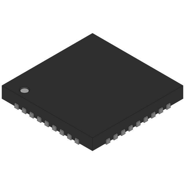


 工商网监
湘ICP备2023018690号
工商网监
湘ICP备2023018690号