User's Guide
SNVA479B – April 2011 – Revised April 2013
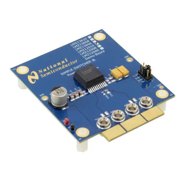
AN-2136 LMZ13610/8/6 and LMZ12010/8/6 Demo Board
1
Introduction
The LMZ13610/8/6 and LMZ12010/8/6 SIMPLE SWITCHER® power modules are easy-to-use DC-DC
solution capable of driving up to a 10, 8 or 6 ampere load. They are available in an innovative package
that enhances thermal performance and allows for hand or machine soldering. The LMZ13610/8/6 can
accept an input voltage rail between 6V and 36V and the LMZ12010/8/6 can accept an input voltage rail
between 6V and 20V.
The demo board is highly configurable. The output voltage can be adjusted to 5V, 3.3V, 2.5V or 1.2V with
a jumper change. The external soft-start capacitor facilitates a controlled and adjustable startup rise time
of the output. The input voltage UVLO can also be adjusted by changing one resistor.
The LMZ13610 and LMZ12010 family is a reliable and robust solution with the following features: loss-less
cycle-by-cycle valley current limit to protect for over current or short-circuit fault, thermal shutdown, input
under-voltage lockout, and will start up into a pre-biased output.
2
Board Specifications
•
•
•
•
•
•
•
VIN = 6V to 36V (LMZ13610/8/6)
VIN = 6V to 20V (LMZ12010/8/6)
VOUT = 1.2V, 2.5V, 3.3V or 5V (minimum input voltage of 7V required for 5V output)
IOUT = 0 to 10, 8, or 6 Amps
θJA = 9.9 °C / W, θJC = 1.0 °C/W
Designed on four layers; Inner are 1 oz copper; Outer are 2 oz copper.
Measures 2.95" × 3.54" (75 mm × 90 mm) and is 62 mils (1.57 mm) thick of FR4 laminate material
For additional circuit considerations, including additional output voltage options, refer to the Applications
Section of the LMZ13610/8/6 or LMZ12010/8/6 data sheets. For negative output voltage connections, see
AN-2027 Inverting Application for the LMZ14203 SIMPLE SWITCHER Power Module Application Report
(SNVA425).
SIMPLE SWITCHER is a registered trademark of Texas Instruments.
All other trademarks are the property of their respective owners.
SNVA479B – April 2011 – Revised April 2013
Submit Documentation Feedback
AN-2136 LMZ13610/8/6 and LMZ12010/8/6 Demo Board
Copyright © 2011–2013, Texas Instruments Incorporated
1
�Board Specifications
www.ti.com
CIN6
(OPT)
+
CIN2,3,4
CIN5
(OPT)
VOUT
SS
FB
PGND
AGND
VIN
EN
VIN
LMZ Module
VOUT
RENT
CIN1
CO3,4
(OPT)
CO1
CSS
CO2
(OPT)
(OPT)
RFBB
RFB_LP
CFF
TEMP
SENSE
D1
5.1V
(OPT)
RENB
CO5
(OPT)
RFBT_5
RFBT_5b
RFBT_3.3
RFBT_3.3b
RFBT_2.5
RFBT_2.5b
RFBT_1.2
RFBT_1.2b
5Vout
3.3Vout
2.5Vout
RTS
1.2Vout
VOUT SELECT
(J1)
Figure 1. Simplified Schematic
2
AN-2136 LMZ13610/8/6 and LMZ12010/8/6 Demo Board
Copyright © 2011–2013, Texas Instruments Incorporated
SNVA479B – April 2011 – Revised April 2013
Submit Documentation Feedback
�Test Connections
www.ti.com
3
Test Connections
The board should be connected to a power supply and load as shown below in Figure 2. The EN post is
connected to the UVLO circuit on the back of the board. There is a resistive divider implemented on the
board that can be used to establish a precision UVLO level for the board that is currently set to 5.7V. A
common user change to this circuit is to adjust the value of RENT and RENB to adjust the operating
UVLO to that of the target application. Refer to the respective data sheet for calculation. Note that if in the
end application the EN pin voltage does not exceed 5.5V at maximum Vin, then the enable clamp zener
D1 can be omitted. (On revision A of the board the overlay for the zener diode has the cathode and anode
incorrectly labeled) Pull EN low to shutdown the module.
Oscilloscope
J1
ABC
ENABLE
VOUT
VIN
ELECTRONIC
LOAD
POWER SUPPLY
Vin = 6 ± 20
(36)V
Set from 0 to 10 Amperes
MULTI-METER
MULTI-METER
Vout = 5, 3.3,
2.5, 1.2V
GND
Figure 2. Board Connection Diagram
SNVA479B – April 2011 – Revised April 2013
Submit Documentation Feedback
AN-2136 LMZ13610/8/6 and LMZ12010/8/6 Demo Board
Copyright © 2011–2013, Texas Instruments Incorporated
3
�Pin Descriptions
4
www.ti.com
Pin Descriptions
The Demo board is also compatible with the 20-pin edge connector shown in Figure 3. The functionality of
the pins is described in Table 1.
I
I
I
I
VOUT
I
I
I
I
GND
I
VIN
9
10
10
A
B
C
D
E
F
H
J
K
L
TEMP SENSE
8
VOUT SENSE +
7
NC
6
AGND
5
VIN SENSE -
4
VOUT SENSE -
3
AGND
2
EN
1
AGND
VIN SENSE +
I
I
I
I
I
I
I
I
I
I
I
Figure 3. Edge Connector Diagram
Table 1. Pin Descriptions
4
Pin
Name
Description
1, 2, 3
VIN
Input supply — Nominal operating range is from 6V to 20V for the LMZ12010/8/6 and
from 6V to 36V for the LMZ13610/8/6.
4, 5, 6, 7
GND
Power Ground — Electrical path for the power circuits within the module.
8, 9, 10
VOUT
Output Voltage — Regulated 5, 3.3, 2.5 or 1.2V.
A
VIN SENSE +
Positive Kelvin Sense of Input voltage — Tied to VIN pin of the LMZ module.
E
VIN SENSE -
Negative Kelvin Sense of Input voltage — Tied to PGND (EP) of the LMZ module.
L
VOUT SENSE +
Positive Kelvin Sense of Output voltage — Tied to Vout banana jack.
Negative Kelvin Sense of Output voltage — Tied to AGND of the LMZ module.
F
VOUT SENSE -
B, D, H
AGND
J
NC
No Connect — This pin must remain floating, do not ground.
C
EN
Enable — Input to the precision enable comparator of the LMZ Module.
K
TEMP SENSE
AGND Ground — Tied to AGND pin of module.
Connected to top of the Rts temperature sensing resistor (unpopulated). Temperature
measurements can be made by measuring the temperature dependant resistance
between TEMP SENSE and VIN SENSE -. Convert the resistance to temperature with
the following equation: Temperature (C) ≊ 2.6245 × Resistance (Ω) - 262.7
AN-2136 LMZ13610/8/6 and LMZ12010/8/6 Demo Board
Copyright © 2011–2013, Texas Instruments Incorporated
SNVA479B – April 2011 – Revised April 2013
Submit Documentation Feedback
�Adjusting the Output Voltage
www.ti.com
5
Adjusting the Output Voltage
The output voltage of the Demo board is adjusted to either 5V, 3.3V, 2.5V, or 1.2V by moving jumper J1.
For other voltage options, see the datasheet for adjusting the feedback resistors.
6
Optional Components
The Demo board has many options for input and output filtering. CO1, CO2 and CO5 can installed with
47nF or greater ceramic capacitors to further decrease high frequency noise on the output. Similarly, CIN1,
and CIN6 can be installed with 47nF capacitors to provide further high frequency bypass for the input
current.
CIN6
(OPT)
+
CIN2,3,4
CIN5
(OPT)
VOUT
SS
FB
PGND
AGND
VIN
EN
VIN
LMZ Module
VOUT
RENT
CIN1
CO3,4
(OPT)
CSS
CO1
CO2
(OPT)
(OPT)
RFBB
RFB_LP
CFF
TEMP
SENSE
D1
5.1V
(OPT)
RENB
CO5
(OPT)
RFBT_5
RFBT_5b
RFBT_3.3
RFBT_3.3b
5Vout
3.3Vout
RFBT_2.5
RFBT_2.5b
RFBT_1.2
RFBT_1.2b
2.5Vout
RTS
1.2Vout
VOUT SELECT
(J1)
Figure 4. Demo Board Schematic
SNVA479B – April 2011 – Revised April 2013
Submit Documentation Feedback
AN-2136 LMZ13610/8/6 and LMZ12010/8/6 Demo Board
Copyright © 2011–2013, Texas Instruments Incorporated
5
�Bill of Materials
7
www.ti.com
Bill of Materials
Table 2. Bill of Materials (VIN = 6V to 36V (20V), VOUT = 1.2 / 3.3V / 5V, IOUT (MAX) = 10/08/06A)
Designator
U1
6
Description
SIMPLE
SWITCHER®
Case Size
Manufacturer
Manufacturer P/N
Qty
PFM-11
Texas Instruments
LMZ13610/08/06,
LMZ12010/08/06
1
Cin2, Cin3,
Cin4
10 µF, X7S, 50V
1210
TDK
C3225X7S1H106M
3
Cin5
150 µF, Aluminum
Electrolytic, 50V
G
Panasonic
EEE-FK1H151P
1
Co3, Co4
330µF, 6.3V, 0.015
ohm,
2917
Kemet
T520D337M006ATE015
2
Cff
4700 pF, X7R, 50V
0805
Kemet
C0805C472K5RACTU
1
Css
0.15uF, X7R, 10V
0603
Murata
GRM188R71A154KA01D
2
D1
4.7V, 500mW
SOD-123
Vishay
MMSZ4688-V-GS08
1
Rent
4.12k ohm, 1%,
0.125W
0805
Vishay-Dale
CRCW08054K12FKEA
1
Renb
1.27k ohm, 1%,
0.125W
0805
Vishay-Dale
CRCW08051K27FKEA
1
Rfbb
1.07k ohm, 1%,
0.125W
0805
Vishay-Dale
CRCW08051K07FKEA
1
Rfbt_1.2
576 ohm, 1%, 0.125W
0805
Vishay-Dale
CRCW0805576RFKEA
1
Rfbt_1.2b
9.53 ohm, 1%, 0.125W
0805
Vishay-Dale
CRCW08059R53FKEA
1
Rfbt_2.5
3.74k ohm, 1%,
0.125W
0805
Vishay-Dale
CRCW08053K74FKEA
1
Rfbt_2.5b
84.5 ohm, 1%, 0.125W
0805
Vishay-Dale
CRCW080584R5FKEA
1
Rfbt_3.3
8.06k ohm, 1%,
0.125W
0805
Vishay-Dale
CRCW08058K06FKEA
1
Rfbt_3.3b
169 ohm, 1%, 0.125W
0805
Vishay-Dale
CRCW0805169RFKEA
1
Rfbt_5
5.6k ohm, 1%, 0.125W
0805
Vishay-Dale
CRCW08055K60FKEA
1
Rfbt_5b
73.2 ohm, 1%, 0.125W
0805
Vishay-Dale
CRCW080573R2FKEA
1
RFB_LP
20 Ω
0805
Vishay-Dale
CRCW080520R0FKEA
1
EN
Test Point, TH,
Miniature, Red
Keystone Electronics
5000
1
GND
Test Point, TH,
Miniature, Black
Keystone Electronics
5001
2
GND, GND,
VIN, VOUT
Banana Jack
Connector
Keystone Electronics
575-8
4
SH-1
Shunt, 100mil, Gold
plated, Black
Amp
382811-6
1
H1, H2, H3, H4
Machine Screw,
Round, #4-40 x 1/4,
Nylon, Philips panhead
B and FFastener
Supply
NY PMS 440 0025 PH
4
H5, H6, H7, H8
Standoff, Hex, 0.5"L
#4-40 Nylon
Keystone
1902C
4
J1
Header, 4x2, Gold
plated, 230 mil above
insulator
Samtec Inc.
TSW-104-07-G-D
1
J2
20-Pin Dual Edge
Connector, 0.156" pitch
EDAC
305-020-500-202
0
Rts
100 ohm, Temp Sense
Resistor
Vishay
PTS08051B100RP 100
0
TH, 100mil
0805
AN-2136 LMZ13610/8/6 and LMZ12010/8/6 Demo Board
Copyright © 2011–2013, Texas Instruments Incorporated
SNVA479B – April 2011 – Revised April 2013
Submit Documentation Feedback
�Performance Characteristics
www.ti.com
8
Performance Characteristics
Thermal Derating, VOUT = 5.0V
12
90
10
OUTPUT CURRENT (A)
EFFICIENCY (%)
Efficiency, VOUT = 5.0V
100
80
70
60
10 Vin
12 Vin
16 Vin
20 Vin
50
40
0
1
2 3 4 5 6 7 8
OUTPUT CURRENT (A)
10A
8A
8
6
4
2
0
9 10
-40 -20 0 20 40 60 80 100 120
AMBIENT TEMPERATURE (°C)
Startup, VIN = 12V, VOUT = 3.3V
Enable
3.3 Vout
1V/Div
TIME (1 ms/Div)
9
Gerber and CAD Files
Gerber and CAD files can be downloaded from the associated product folder.
SNVA479B – April 2011 – Revised April 2013
Submit Documentation Feedback
AN-2136 LMZ13610/8/6 and LMZ12010/8/6 Demo Board
Copyright © 2011–2013, Texas Instruments Incorporated
7
�PCB Layout Diagrams
10
www.ti.com
PCB Layout Diagrams
Figure 5. Top Layer
Figure 6. Internal Layer I (Ground)
Heat Sinking Layer
8
AN-2136 LMZ13610/8/6 and LMZ12010/8/6 Demo Board
Copyright © 2011–2013, Texas Instruments Incorporated
SNVA479B – April 2011 – Revised April 2013
Submit Documentation Feedback
�PCB Layout Diagrams
www.ti.com
Figure 7. Internal Layer II (Routing)
Heat Sinking Layer
Figure 8. Bottom Layer (Ground and Routing)
Heat Sinking Layer
SNVA479B – April 2011 – Revised April 2013
Submit Documentation Feedback
AN-2136 LMZ13610/8/6 and LMZ12010/8/6 Demo Board
Copyright © 2011–2013, Texas Instruments Incorporated
9
�PCB Layout Diagrams
www.ti.com
Figure 9. Top Silkscreen
Figure 10. Bottom Silkscreen
10
AN-2136 LMZ13610/8/6 and LMZ12010/8/6 Demo Board
Copyright © 2011–2013, Texas Instruments Incorporated
SNVA479B – April 2011 – Revised April 2013
Submit Documentation Feedback
�IMPORTANT NOTICE
Texas Instruments Incorporated and its subsidiaries (TI) reserve the right to make corrections, enhancements, improvements and other
changes to its semiconductor products and services per JESD46, latest issue, and to discontinue any product or service per JESD48, latest
issue. Buyers should obtain the latest relevant information before placing orders and should verify that such information is current and
complete. All semiconductor products (also referred to herein as “components”) are sold subject to TI’s terms and conditions of sale
supplied at the time of order acknowledgment.
TI warrants performance of its components to the specifications applicable at the time of sale, in accordance with the warranty in TI’s terms
and conditions of sale of semiconductor products. Testing and other quality control techniques are used to the extent TI deems necessary
to support this warranty. Except where mandated by applicable law, testing of all parameters of each component is not necessarily
performed.
TI assumes no liability for applications assistance or the design of Buyers’ products. Buyers are responsible for their products and
applications using TI components. To minimize the risks associated with Buyers’ products and applications, Buyers should provide
adequate design and operating safeguards.
TI does not warrant or represent that any license, either express or implied, is granted under any patent right, copyright, mask work right, or
other intellectual property right relating to any combination, machine, or process in which TI components or services are used. Information
published by TI regarding third-party products or services does not constitute a license to use such products or services or a warranty or
endorsement thereof. Use of such information may require a license from a third party under the patents or other intellectual property of the
third party, or a license from TI under the patents or other intellectual property of TI.
Reproduction of significant portions of TI information in TI data books or data sheets is permissible only if reproduction is without alteration
and is accompanied by all associated warranties, conditions, limitations, and notices. TI is not responsible or liable for such altered
documentation. Information of third parties may be subject to additional restrictions.
Resale of TI components or services with statements different from or beyond the parameters stated by TI for that component or service
voids all express and any implied warranties for the associated TI component or service and is an unfair and deceptive business practice.
TI is not responsible or liable for any such statements.
Buyer acknowledges and agrees that it is solely responsible for compliance with all legal, regulatory and safety-related requirements
concerning its products, and any use of TI components in its applications, notwithstanding any applications-related information or support
that may be provided by TI. Buyer represents and agrees that it has all the necessary expertise to create and implement safeguards which
anticipate dangerous consequences of failures, monitor failures and their consequences, lessen the likelihood of failures that might cause
harm and take appropriate remedial actions. Buyer will fully indemnify TI and its representatives against any damages arising out of the use
of any TI components in safety-critical applications.
In some cases, TI components may be promoted specifically to facilitate safety-related applications. With such components, TI’s goal is to
help enable customers to design and create their own end-product solutions that meet applicable functional safety standards and
requirements. Nonetheless, such components are subject to these terms.
No TI components are authorized for use in FDA Class III (or similar life-critical medical equipment) unless authorized officers of the parties
have executed a special agreement specifically governing such use.
Only those TI components which TI has specifically designated as military grade or “enhanced plastic” are designed and intended for use in
military/aerospace applications or environments. Buyer acknowledges and agrees that any military or aerospace use of TI components
which have not been so designated is solely at the Buyer's risk, and that Buyer is solely responsible for compliance with all legal and
regulatory requirements in connection with such use.
TI has specifically designated certain components as meeting ISO/TS16949 requirements, mainly for automotive use. In any case of use of
non-designated products, TI will not be responsible for any failure to meet ISO/TS16949.
Products
Applications
Audio
www.ti.com/audio
Automotive and Transportation
www.ti.com/automotive
Amplifiers
amplifier.ti.com
Communications and Telecom
www.ti.com/communications
Data Converters
dataconverter.ti.com
Computers and Peripherals
www.ti.com/computers
DLP® Products
www.dlp.com
Consumer Electronics
www.ti.com/consumer-apps
DSP
dsp.ti.com
Energy and Lighting
www.ti.com/energy
Clocks and Timers
www.ti.com/clocks
Industrial
www.ti.com/industrial
Interface
interface.ti.com
Medical
www.ti.com/medical
Logic
logic.ti.com
Security
www.ti.com/security
Power Mgmt
power.ti.com
Space, Avionics and Defense
www.ti.com/space-avionics-defense
Microcontrollers
microcontroller.ti.com
Video and Imaging
www.ti.com/video
RFID
www.ti-rfid.com
OMAP Applications Processors
www.ti.com/omap
TI E2E Community
e2e.ti.com
Wireless Connectivity
www.ti.com/wirelessconnectivity
Mailing Address: Texas Instruments, Post Office Box 655303, Dallas, Texas 75265
Copyright © 2013, Texas Instruments Incorporated
�