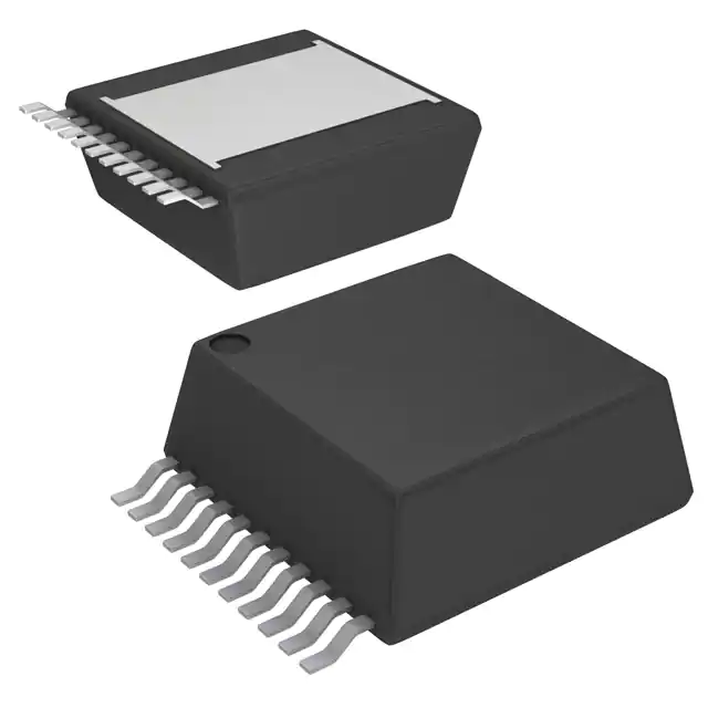
LMZ12010
SNVS667I – FEBRUARY 2010 – REVISED MARCH 2022
LMZ12010 10-A SIMPLE SWITCHER® Power Module With 20-V Maximum Input Voltage
1 Features
2 Applications
•
•
•
•
•
•
•
Point-of-load conversions from 12-V input rail
Time-critical projects
Space-constrained and high thermal requirement
applications
Negative output voltage applications
(See AN-2027 SNVA425)
•
3 Description
The LMZ12010 SIMPLE SWITCHER® power module
is an easy-to-use step-down DC-DC solution capable
of driving up to 10-A load. The LMZ12010 is
available in an innovative package that enhances
thermal performance and allows for hand or machine
soldering.
The LMZ12010 device can accept an input voltage rail
between 6 V and 20 V and deliver an adjustable and
highly accurate output voltage as low as 0.8 V. The
LMZ12010 only requires two external resistors and
external capacitors to complete the power solution.
The LMZ12010 is a reliable and robust design with
the following protection features: thermal shutdown,
programmable input undervoltage lockout, output
overvoltage protection, short circuit protection, output
current limit, and the device allows start-up into a
prebiased output.
Device Information
PART
NUMBER(2)
LMZ12010
(1)
(2)
BODY SIZE (NOM)
NDY (11)
15.00 mm × 15.00 mm
100
90
VOUT
VOUT
EFFICIENCY (%)
SS
VIN
PACKAGE(1)
For all available packages, see the orderable addendum at
the end of the data sheet.
Peak reflow temperature equals 245°C. See SNAA214 for
more details.
LMZ12010
FB
•
AGND
•
PGND
•
•
EN
•
•
VIN
•
Integrated shielded inductor
Simple PCB layout
Fixed switching frequency (350 kHz)
Flexible start-up sequencing using external soft
start, tracking, and precision enable
Protection against inrush currents and faults such
as input UVLO and output short circuit
Junction temperature range: –40°C to 125°C
Single exposed pad and standard pinout for easy
mounting and manufacturing
Fully enabled for WEBENCH® power designer
Pin compatible with LMZ22010, LMZ22008,
LMZ22006, LMZ12008, LMZ12006, LMZ23610,
LMZ23608, LMZ23606, LMZ13610, LMZ13608,
and LMZ13606
Electrical specifications
– 50-W maximum total output power
– Up to 10-A output current
– Input voltage range: 6 V to 20 V
– Output voltage range: 0.8 V to 6 V
– Efficiency up to 92%
Performance benefits
– High efficiency reduces system heat generation
– Low radiated emissions (EMI) tested to
EN55022 1
– Only seven external components
– Low output voltage ripple
– No external heat sink required
CFF 4.7 nF (OPT)
Enable
RFBT
80
70
60
6 Vin
10 Vin
12 Vin
16 Vin
20 Vin
See Table
CIN
3 x 10 PF
CSS
0.47 PF
(OPT)
RFBB
See Table
COUT
2 x 330 PF
Simplified Application Schematic
50
40
0
1
2 3 4 5 6 7 8
OUTPUT CURRENT (A)
9 10
Efficiency 3.3-V Output at 25°C
1
EN 55022:2006, +A1:2007, FCC Part 15 Subpart B, tested on Evaluation Board with EMI configuration.
An IMPORTANT NOTICE at the end of this data sheet addresses availability, warranty, changes, use in safety-critical applications,
intellectual property matters and other important disclaimers. PRODUCTION DATA.
�LMZ12010
www.ti.com
SNVS667I – FEBRUARY 2010 – REVISED MARCH 2022
Table of Contents
1 Features............................................................................1
2 Applications..................................................................... 1
3 Description.......................................................................1
4 Revision History.............................................................. 2
5 Pin Configuration and Functions...................................3
6 Specifications.................................................................. 4
6.1 Absolute Maximum Ratings ....................................... 4
6.2 ESD Ratings............................................................... 4
6.3 Recommended Operating Conditions.........................4
6.4 Thermal Information....................................................4
6.5 Electrical Characteristics.............................................5
6.6 Typical Characteristics................................................ 6
7 Detailed Description......................................................14
7.1 Overview................................................................... 14
7.2 Functional Block Diagram......................................... 14
7.3 Feature Description...................................................14
7.4 Device Functional Modes..........................................15
8 Application and Implementation.................................. 17
8.1 Application Information............................................. 17
8.2 Typical Application.................................................... 17
9 Power Supply Recommendations................................23
10 Layout...........................................................................24
10.1 Layout Guidelines................................................... 24
10.2 Layout Examples.................................................... 24
10.3 Power Dissipation and Thermal Considerations..... 26
10.4 Power Module SMT Guidelines.............................. 27
11 Device and Documentation Support..........................29
11.1 Device Support........................................................29
11.2 Documentation Support.......................................... 29
11.3 Support Resources................................................. 29
11.4 Receiving Notification of Documentation Updates.. 29
11.5 Trademarks............................................................. 29
11.6 Electrostatic Discharge Caution.............................. 29
11.7 Glossary.................................................................. 30
12 Mechanical, Packaging, and Orderable
Information.................................................................... 30
4 Revision History
NOTE: Page numbers for previous revisions may differ from page numbers in the current version.
Changes from Revision H (July 2015) to Revision I (March 2022)
Page
• Updated the numbering format for tables, figures, and cross-references throughout the document. ................1
• Corrected AGND pin 2 to AGND pin 3................................................................................................................3
Changes from Revision G (October 2013) to Revision H (July 2015)
Page
• Added Pin Configuration and Functions section, ESD Ratings table, Feature Description section, Device
Functional Modes, Application and Implementation section, Power Supply Recommendations section, Layout
section, Device and Documentation Support section, and Mechanical, Packaging, and Orderable Information
section ............................................................................................................................................................... 1
2
Submit Document Feedback
Copyright © 2022 Texas Instruments Incorporated
Product Folder Links: LMZ12010
�LMZ12010
www.ti.com
SNVS667I – FEBRUARY 2010 – REVISED MARCH 2022
5 Pin Configuration and Functions
PGND/EP
Connect to AGND
11
10
9
8
7
6
5
4
3
2
1
VOUT
VOUT
NC
SS
FB
AGND
AGND
EN
AGND
VIN
VIN
Figure 5-1. 11-Pin NDY Package (Top View)
Table 5-1. Pin Functions
PIN
NAME
NO.
TYPE
DESCRIPTION
Ground
Analog ground — Reference point for all stated voltages. Must be externally connected to PGND
(EP).
3
AGND
5
6
EN
4
Analog
Enable — Input to the precision enable comparator. Rising threshold is 1.274 V (typical). Once
the module is enabled, a 13-µA source current is internally activated to facilitate programmable
hysteresis.
FB
7
Analog
Feedback — Internally connected to the regulation amplifier and overvoltage comparator. The
regulation reference point is 0.795 V at this input pin. Connect the feedback resistor divider
between VOUT and AGND to set the output voltage.
NC
9
—
PGND
—
Ground
Exposed pad/power ground — Electrical path for the power circuits within the module. PGND
is not internally connected to AGND (pin 5, 6). Must be electrically connected to pins 5 and 6
external to the package. The exposed pad is also used to dissipate heat from the package during
operation. Use 100 12-mil thermal vias from top to bottom copper for best thermal performance.
SS
8
Analog
Soft-start/track input — To extend the 1.6-ms internal soft start, connect an external soft-start
capacitor. For tracking, connect to an external resistive divider to a higher priority supply rail. See
Section 8.2.2.
Power
Input supply — Nominal operating range is 6 V to 20 V. A small amount of internal capacitance
is contained within the package assembly. Additional external input capacitance is required
between this pin and the exposed pad (PGND).
Power
Output voltage — Output from the internal inductor. Connect the output capacitor between this
pin and exposed pad (PGND).
1
VIN
VOUT
2
10
11
No connect — This pin must remain floating, do not ground.
Submit Document Feedback
Copyright © 2022 Texas Instruments Incorporated
Product Folder Links: LMZ12010
3
�LMZ12010
www.ti.com
SNVS667I – FEBRUARY 2010 – REVISED MARCH 2022
6 Specifications
6.1 Absolute Maximum Ratings
MIN(1) (2)
MAX(1) (2)
UNIT
VIN to PGND
–0.3
24
V
EN to AGND
–0.3
5.5
V
SS, FB to AGND
–0.3
2.5
V
AGND to PGND
–0.3
Junction Temperature
Peak reflow case temperature (30 sec)
Storage temperature, Tstg
(1)
(2)
–65
0.3
V
150
°C
245
°C
150
°C
Stresses beyond those listed under Absolute Maximum Ratings may cause permanent damage to the device. These are stress
ratings only, which do not imply functional operation of the device at these or any other conditions beyond those indicated under
Recommended Operating Conditions. Exposure to absolute-maximum-rated conditions for extended periods may affect device
reliability.
For soldering specifications, refer to the Absolute Maximum Ratings for Soldering application report.
6.2 ESD Ratings
V(ESD)
(1)
(2)
Electrostatic discharge
Human body model (HBM), per ANSI/ESDA/JEDEC
JS-001(1) (2)
VALUE
UNIT
±2000
V
JEDEC document JEP155 states that 500-V HBM allows safe manufacturing with a standard ESD control process.
The human body model is a 100-pF capacitor discharged through a 1.5-kΩ resistor into each pin. Test method is per JESD-22-114.
6.3 Recommended Operating Conditions
VIN
EN
Operation junction temperature
(1)
MIN(1)
MAX(1)
6
20
UNIT
V
0
5
V
−40
125
°C
Absolute Maximum Ratings are limits beyond which damage to the device may occur. Operating Ratings are conditions under which
operation of the device is intended to be functional. For compliant specifications and test conditions, see the Electrical Characteristics.
6.4 Thermal Information
LMZ12010
THERMAL METRIC(1)
NDY
UNIT
11 PINS
Junction-to-ambient thermal
resistance
RθJA
RθJC(top)
(1)
4
Natural Convection
9.9
225 LFPM
6.8
500 LFPM
5.2
Junction-to-case (top) thermal resistance
1.0
°C/W
°C/W
For more information about traditional and new thermal metrics, see the Semiconductor and IC Package Thermal Metrics application
report, SPRA953.
Submit Document Feedback
Copyright © 2022 Texas Instruments Incorporated
Product Folder Links: LMZ12010
�LMZ12010
www.ti.com
SNVS667I – FEBRUARY 2010 – REVISED MARCH 2022
6.5 Electrical Characteristics
Limits are for TJ = 25°C unless otherwise specified. Minimum and Maximum limits are ensured through test, design or
statistical correlation. Typical values represent the most likely parametric norm at TJ = 25°C, and are provided for reference
purposes only. Unless otherwise stated the following conditions apply: VIN = 12 V, VOUT = 3.3 V
PARAMETER
TEST CONDITIONS
MIN
TYP
MAX UNIT
SYSTEM PARAMETERS
ENABLE CONTROL
1.274
VEN
EN threshold
VEN rising
IEN-HYS
EN hysteresis source
current
VEN > 1.274 V
ISS
SS source current
VSS = 0 V
tSS
Internal soft-start interval
Over the junction temperature (TJ)
range of –40°C to +125°C
1.096
V
1.452
13
µA
SOFT-START
50
Over the junction temperature (TJ)
range of –40°C to +125°C
40
60
1.6
µA
ms
CURRENT LIMIT
ICL
Current limit threshold
DC average
12.5
A
INTERNAL SWITCHING OSCILLATOR
Free-running oscillator
frequency
fosc
314
359
404
kHz
REGULATION AND OVERVOLTAGE COMPARATOR
VFB
In-regulation feedback
voltage
VFB-OV
Feedback overvoltage
protection threshold
IFB
VSS >+ 0.8 V
IO = 10 A
0.795
over the junction temperature (TJ)
range of –40°C to +125°C
0.775
V
0.815
0.86
V
Feedback input bias
current
5
nA
IQ
Nonswitching quiescent
current
3
mA
ISD
Shutdown quiescent
current
32
μA
Dmax
Maximum duty factor
VEN = 0 V
85%
THERMAL CHARACTERISTICS
TSD
Thermal shutdown
Rising
165
°C
TSD-HYST
Thermal shutdown
hysteresis
Falling
15
°C
24
mVPP
PERFORMANCE PARAMETERS (1)
ΔVO
Output voltage ripple
BW at 20 MHz
ΔVO/ΔVIN
Line regulation
VIN = 12 V to 20 V, IOUT= 10 A
ΔVO/ΔIOUT
Load regulation
VIN = 12 V, IOUT= 0.001 A to 10 A
η
Peak efficiency
VIN = 12 V, VOUT = 3.3 V, IOUT = 5 A
89.5%
η
Full load efficiency
VIN = 12 V, VOUT = 3.3 V, IOUT = 10 A
87.5%
(1)
±0.2%
1
mV/A
EN 55022:2006, +A1:2007, FCC Part 15 Subpart B, tested on Evaluation Board with EMI configuration.
Submit Document Feedback
Copyright © 2022 Texas Instruments Incorporated
Product Folder Links: LMZ12010
5
�LMZ12010
www.ti.com
SNVS667I – FEBRUARY 2010 – REVISED MARCH 2022
6.6 Typical Characteristics
Unless otherwise specified, the following conditions apply: VIN = 12 V; CIN = three × 10-μF + 47-nF X7R
Ceramic; COUT = two × 330-μF Specialty Polymer + 47-μF Ceramic + 47-nF Ceramic; CFF = 4.7 nF; TA = 25°C
for waveforms. All indicated temperatures are ambient.
100
8
DISSIPATION (W)
EFFICIENCY (%)
90
80
70
60
8 Vin
10 Vin
12 Vin
16 Vin
20 Vin
50
40
0
2
4
6
8
OUTPUT CURRENT (A)
4
3
2
0
0
8
DISSIPATION (W)
70
60
6 Vin
10 Vin
12 Vin
16 Vin
20 Vin
50
40
0
1
2 3 4 5 6 7 8
OUTPUT CURRENT (A)
6
5
4
3
2
9 10
0
DISSIPATION (W)
90
70
60
6 Vin
10 Vin
12 Vin
16 Vin
20 Vin
1
2 3 4 5 6 7 8
OUTPUT CURRENT (A)
2 3 4 5 6 7 8
OUTPUT CURRENT (A)
9
10
6 Vin
10 Vin
12 Vin
16 Vin
20 Vin
7
80
1
Figure 6-4. Dissipation 3.3-V Output at 25°C
8
0
10
0
100
40
9
1
Figure 6-3. Efficiency 3.3-V Output at 25°C
50
2 3 4 5 6 7 8
OUTPUT CURRENT (A)
6 Vin
10 Vin
12 Vin
16 Vin
20 Vin
7
80
1
Figure 6-2. Dissipation 5-V Output at 25°C
90
EFFICIENCY (%)
5
10
100
EFFICIENCY (%)
6
1
Figure 6-1. Efficiency 5-V Output at 25°C
6
5
4
3
2
1
0
9 10
Figure 6-5. Efficiency 2.5-V Output at 25°C
6
8 Vin
10 Vin
12 Vin
16 Vin
20 Vin
7
0
1
2 3 4 5 6 7 8
OUTPUT CURRENT (A)
9
10
Figure 6-6. Dissipation 2.5-V Output at 25°C
Submit Document Feedback
Copyright © 2022 Texas Instruments Incorporated
Product Folder Links: LMZ12010
�LMZ12010
SNVS667I – FEBRUARY 2010 – REVISED MARCH 2022
90
8
80
7
DISSIPATION (W)
EFFICIENCY (%)
www.ti.com
70
60
50
40
6 Vin
10 Vin
12 Vin
16 Vin
20 Vin
30
20
0
1
2 3 4 5 6 7 8
OUTPUT CURRENT (A)
4
3
2
0
9 10
0
8
80
7
70
60
50
6 Vin
10 Vin
12 Vin
16 Vin
20 Vin
20
0
1
2 3 4 5 6 7 8
OUTPUT CURRENT (A)
4
3
2
0
9 10
0
DISSIPATION (W)
80
70
60
50
6 Vin
10 Vin
12 Vin
16 Vin
20 Vin
1
2 3 4 5 6 7 8
OUTPUT CURRENT (A)
1
2 3 4 5 6 7 8
OUTPUT CURRENT (A)
9
10
Figure 6-10. Dissipation 1.5-V Output at 25°C
7
0
10
5
8
20
9
6 Vin
10 Vin
12 Vin
16 Vin
20 Vin
6
90
30
2 3 4 5 6 7 8
OUTPUT CURRENT (A)
1
Figure 6-9. Efficiency 1.5-V Output at 25°C
40
1
Figure 6-8. Dissipation 1.8-V Output at 25°C
DISSIPATION (W)
EFFICIENCY (%)
5
90
30
EFFICIENCY (%)
6
1
Figure 6-7. Efficiency 1.8-V Output at 25°C
40
6 Vin
10 Vin
12 Vin
16 Vin
20 Vin
6 Vin
10 Vin
12 Vin
16 Vin
20 Vin
6
5
4
3
2
1
0
9 10
Figure 6-11. Efficiency 1.2-V Output at 25°C
0
1
2 3 4 5 6 7 8
OUTPUT CURRENT (A)
9
10
Figure 6-12. Dissipation 1.2-V Output at 25°C
Submit Document Feedback
Copyright © 2022 Texas Instruments Incorporated
Product Folder Links: LMZ12010
7
�LMZ12010
www.ti.com
90
8
80
7
70
6
DISSIPATION (W)
EFFICIENCY (%)
SNVS667I – FEBRUARY 2010 – REVISED MARCH 2022
60
50
40
6 Vin
10 Vin
12 Vin
16 Vin
20 Vin
30
20
10
0
1
2 3 4 5 6 7 8
OUTPUT CURRENT (A)
3
2
9 10
0
8
DISSIPATION (W)
70
60
8 Vin
10 Vin
12 Vin
16 Vin
20 Vin
50
40
0
1
2 3 4 5 6 7 8
OUTPUT CURRENT (A)
6
4
3
2
0
9 10
0
7
80
6
DISSIPATION (W)
90
70
60
50
6 Vin
10 Vin
12 Vin
16 Vin
20 Vin
0
1
2 3 4 5 6 7 8
OUTPUT CURRENT (A)
1
2 3 4 5 6 7 8
OUTPUT CURRENT (A)
9
10
Figure 6-16. Dissipation 5-V Output at 85°C
8
20
10
5
100
30
9
1
Figure 6-15. Efficiency 5-V Output at 85°C
40
2 3 4 5 6 7 8
OUTPUT CURRENT (A)
8 Vin
10 Vin
12 Vin
16 Vin
20 Vin
7
80
1
Figure 6-14. Dissipation 1-V Output at 25°C
90
EFFICIENCY (%)
4
0
100
EFFICIENCY (%)
5
1
Figure 6-13. Efficiency 1-V Output at 25°C
6 Vin
10 Vin
12 Vin
16 Vin
20 Vin
5
4
3
2
1
0
9 10
Figure 6-17. Efficiency 3.3-V Output at 85°C
8
6 Vin
10 Vin
12 Vin
16 Vin
20 Vin
0
1
2 3 4 5 6 7 8
OUTPUT CURRENT (A)
9
10
Figure 6-18. Dissipation 3.3-V Output at 85°C
Submit Document Feedback
Copyright © 2022 Texas Instruments Incorporated
Product Folder Links: LMZ12010
�LMZ12010
SNVS667I – FEBRUARY 2010 – REVISED MARCH 2022
100
8
90
7
80
6
DISSIPATION (W)
EFFICIENCY (%)
www.ti.com
70
60
50
6 Vin
10 Vin
12 Vin
16 Vin
20 Vin
40
30
20
0
1
2 3 4 5 6 7 8
OUTPUT CURRENT (A)
3
2
0
9 10
0
8
80
7
70
6
60
50
40
6 Vin
10 Vin
12 Vin
16 Vin
20 Vin
10
0
1
2 3 4 5 6 7 8
OUTPUT CURRENT (A)
2
0
9 10
0
6
DISSIPATION (W)
70
60
50
40
6 Vin
10 Vin
12 Vin
16 Vin
20 Vin
2 3 4 5 6 7 8
OUTPUT CURRENT (A)
1
2 3 4 5 6 7 8
OUTPUT CURRENT (A)
9
10
Figure 6-22. Dissipation 1.8-V Output at 85°C
7
1
6 Vin
10 Vin
12 Vin
16 Vin
20 Vin
3
80
0
10
4
8
10
9
5
90
20
2 3 4 5 6 7 8
OUTPUT CURRENT (A)
1
Figure 6-21. Efficiency 1.8-V Output at 85°C
30
1
Figure 6-20. Dissipation 2.5-V Output at 85°C
DISSIPATION (W)
EFFICIENCY (%)
4
90
20
EFFICIENCY (%)
5
1
Figure 6-19. Efficiency 2.5-V Output at 85°C
30
6 Vin
10 Vin
12 Vin
16 Vin
20 Vin
6 Vin
10 Vin
12 Vin
16 Vin
20 Vin
5
4
3
2
1
0
9 10
Figure 6-23. Efficiency 1.5-V Output at 85°C
0
1
2 3 4 5 6 7 8
OUTPUT CURRENT (A)
9
10
Figure 6-24. Dissipation 1.5-V Output at 85°C
Submit Document Feedback
Copyright © 2022 Texas Instruments Incorporated
Product Folder Links: LMZ12010
9
�LMZ12010
www.ti.com
90
8
80
7
70
6
DISSIPATION (W)
EFFICIENCY (%)
SNVS667I – FEBRUARY 2010 – REVISED MARCH 2022
60
50
40
6 Vin
10 Vin
12 Vin
16 Vin
20 Vin
30
20
10
0
1
2 3 4 5 6 7 8
OUTPUT CURRENT (A)
3
2
0
9 10
0
8
80
7
70
6
60
50
40
6 Vin
10 Vin
12 Vin
16 Vin
20 Vin
10
0
1
2 3 4 5 6 7 8
OUTPUT CURRENT (A)
4
3
2
0
1
2 3 4 5 6 7 8
OUTPUT CURRENT (A)
9
10
Figure 6-28. Dissipation 1-V Output at 85°C
MAXIMUM OUTPUT CURRENT (A)
0.998
10
8
6
4
2
JA = 9.9 °C/W
JA = 6.8 °C/W
JA = 5.2 °C/W
0
10
20
VOUT = 3.3 V
40
60
80
100
TEMPERATURE (C)
120
VIN = 12 V, VOUT = 5 V
Figure 6-29. Normalized Line and Load Regulation
10
6 Vin
10 Vin
12 Vin
16 Vin
20 Vin
12
0.999
2
4
6
8
OUTPUT CURRENT (A)
10
0
1.000
0
9
5
9 10
6 Vin
8 Vin
10 Vin
12 Vin
16 Vin
20 Vin
1.001
2 3 4 5 6 7 8
OUTPUT CURRENT (A)
1
Figure 6-27. Efficiency 1-V Output at 85°C
1.002
1
Figure 6-26. Dissipation 1.2-V Output at 85°C
DISSIPATION (W)
EFFICIENCY (%)
4
90
20
NORMALIZED VOUT (V/V)
5
1
Figure 6-25. Efficiency 1.2-V Output at 85°C
30
6 Vin
10 Vin
12 Vin
16 Vin
20 Vin
Figure 6-30. Thermal Derating
Submit Document Feedback
Copyright © 2022 Texas Instruments Incorporated
Product Folder Links: LMZ12010
�LMZ12010
www.ti.com
SNVS667I – FEBRUARY 2010 – REVISED MARCH 2022
30
2 Layer 0 LFPM
2 Layer 225 LFPM
4 Layer 0 LFPM
4 Layer 225 LFPM
27
10
24
THETA JA (°C/W)
MAXIMUM OUTPUT CURRENT (A)
12
8
6
4
21
18
15
12
9
2
JA = 9.9 °C/W
JA = 6.8 °C/W
JA = 5.2 °C/W
0
20
40
6
3
60
80
100
TEMPERATURE (C)
120
0
2
4
6
8
2
COPPER AREA (in )
10
12
Figure 6-32. RθJA vs Copper Heat Sinking Area
VIN = 12 V, VOUT = 3.3 V
Figure 6-31. Thermal Derating
12 VIN, 5 VOUT at Full Load, BW = 20 MHz
12 VIN, 5 VOUT at Full Load, BW = 250 MHz
Figure 6-33. Output Ripple
Figure 6-34. Output Ripple
12 VIN, 3.3 VOUT at Full Load, BW = 20 MHz
12 VIN, 3.3 VOUT at Full Load, BW = 250 MHz
Figure 6-36. Output Ripple
Figure 6-35. Output Ripple
Submit Document Feedback
Copyright © 2022 Texas Instruments Incorporated
Product Folder Links: LMZ12010
11
�LMZ12010
www.ti.com
SNVS667I – FEBRUARY 2010 – REVISED MARCH 2022
12 VIN, 1.2 VOUT at Full Load, BW = 250 MHz
12 VIN, 1.2 VOUT at Full Load, BW = 20 MHz
Figure 6-38. Output Ripple
Figure 6-37. Output Ripple
12 VIN, 5 VOUT 1- to 10-A Step
12 VIN, 3.3 VOUT 1- to 10-A Step
Figure 6-39. Transient Response
Figure 6-40. Transient Response
16
14
CURRENT (A)
12
10
8
6
4
Output Current
Input Current
2
0
12 VIN, 1.2 VOUT 1- to 10-A Step
5
Figure 6-41. Transient Response
10
15
INPUT VOLTAGE (V)
20
Figure 6-42. Short Circuit Current vs Input Voltage
12
Submit Document Feedback
Copyright © 2022 Texas Instruments Incorporated
Product Folder Links: LMZ12010
�LMZ12010
www.ti.com
SNVS667I – FEBRUARY 2010 – REVISED MARCH 2022
No CSS
CSS = 0.47 µF
Figure 6-43. 3.3-VOUT Soft Start
Figure 6-44. 3.3-VOUT Soft Start
Submit Document Feedback
Copyright © 2022 Texas Instruments Incorporated
Product Folder Links: LMZ12010
13
�LMZ12010
www.ti.com
SNVS667I – FEBRUARY 2010 – REVISED MARCH 2022
7 Detailed Description
7.1 Overview
The architecture used is an internally compensated emulated peak current mode control, based on a monolithic
synchronous SIMPLE SWITCHER core capable of supporting high load currents. The output voltage is
maintained through feedback compared with an internal 0.8-V reference. For emulated peak current mode, the
valley current is sampled on the down-slope of the inductor current. This is used as the DC value of current to
start the next cycle. The primary application for emulated peak current mode is high input voltage to low output
voltage operating at a narrow duty cycle. By sampling the inductor current at the end of the switching cycle and
adding an external ramp, the minimum on time can be significantly reduced, without the need for blanking or
filtering, which is normally required for peak current mode control.
7.2 Functional Block Diagram
Linear
Regulator
2M
VIN
1
3
3
CIN
EN
CBST
CINint
1
2.2 uH VOUT
VREF
3
RFBT
CSS
2
350 kHz
PWM
SS
COUT
FB
2
Comp
RFBB
AGND
Regulator IC
EP/
PGND
Internal Passives
7.3 Feature Description
7.3.1 Output Overvoltage Protection
If the voltage at FB is greater than a 0.86-V internal reference, the output of the error amplifier is pulled toward
ground, causing VOUT to fall.
7.3.2 Current Limit
The LMZ12010 is protected by both low-side (LS) and high-side (HS) current limit circuitry. The LS current limit
detection is carried out during the off time by monitoring the current through the LS synchronous MOSFET.
Referring to the Functional Block Diagram, when the top MOSFET is turned off, the inductor current flows
through the load, the PGND pin, and the internal synchronous MOSFET. If this current exceeds 13 A (typical),
the current limit comparator disables the start of the next switching period. Switching cycles are prohibited until
current drops below the limit.
Note
DC current limit is dependent on duty cycle as illustrated in the graph in Section 6.6.
The HS current limit monitors the current of top-side MOSFET. Once HS current limit is detected (16 A typical),
the HS MOSFET is shut off immediately until the next cycle. Exceeding HS current limit causes VOUT to fall.
Typical behavior of exceeding LS current limit is that fSW drops to 1/2 of the operating frequency.
14
Submit Document Feedback
Copyright © 2022 Texas Instruments Incorporated
Product Folder Links: LMZ12010
�LMZ12010
www.ti.com
SNVS667I – FEBRUARY 2010 – REVISED MARCH 2022
7.3.3 Thermal Protection
The junction temperature of the LMZ12010 must not be allowed to exceed its maximum ratings. Thermal
protection is implemented by an internal thermal shutdown circuit, which activates at 165°C (typical), causing the
device to enter a low power standby state. In this state, the main MOSFET remains off, causing VOUT to fall, and
the CSS capacitor is discharged to ground. Thermal protection helps prevent catastrophic failures for accidental
device overheating. When the junction temperature falls back below 150°C (typical hysteresis = 15°C), the SS
pin is released, VOUT rises smoothly, and normal operation resumes.
Applications requiring maximum output current, especially those at high input voltages, can require additional
derating at elevated temperatures.
7.3.4 Prebiased Start-Up
The LMZ12010 will properly start up into a prebiased output. This start-up situation is common in multiple rail
logic applications where current paths can exist between different power rails during the start-up sequence.
Figure 7-1 shows proper behavior in this mode. Trace one is Enable going high. Trace two is 1.8-V prebias rising
to 3.3 V. Trace three is the SS voltage with a CSS = 0.47 µF. Rise time is determined by CSS.
Figure 7-1. Prebiased Start-Up
7.4 Device Functional Modes
7.4.1 Discontinuous Conduction and Continuous Conduction Modes
At light load, the regulator will operate in discontinuous conduction mode (DCM). With load currents above the
critical conduction point, it will operate in continuous conduction mode (CCM). When operating in DCM, inductor
current is maintained to an average value equaling IOUT. In DCM, the low-side switch will turn off when the
inductor current falls to zero. This causes the inductor current to resonate. Although it is in DCM, the current is
allowed to go slightly negative to charge the bootstrap capacitor.
In CCM, current flows through the inductor through the entire switching cycle and never falls to zero during the
off time.
Submit Document Feedback
Copyright © 2022 Texas Instruments Incorporated
Product Folder Links: LMZ12010
15
�LMZ12010
www.ti.com
SNVS667I – FEBRUARY 2010 – REVISED MARCH 2022
Figure 7-2 is a comparison pair of waveforms showing both the CCM (upper) and DCM operating modes.
VIN = 12 V, VO = 3.3 V, IO = 3 A / 0.3 A
Figure 7-2. CCM and DCM Operating Modes
The approximate formula for determining the DCM/CCM boundary is:
IDCB =
(VIN - VOUT) x D
2 x L x fSW
(1)
The inductor internal to the module is 2.2 μH. This value was chosen as a good balance between low and high
input voltage applications. The main parameter affected by the inductor is the amplitude of the inductor ripple
current (ΔiL). ΔiL can be calculated with:
'iL =
(VIN - VOUT) x D
L x fSW
(2)
where
•
•
VIN is the maximum input voltage.
fSW is typically 359 kHz.
If the output current IOUT is determined by assuming that IOUT = IL, the higher and lower peak of ΔiL can be
determined.
16
Submit Document Feedback
Copyright © 2022 Texas Instruments Incorporated
Product Folder Links: LMZ12010
�LMZ12010
www.ti.com
SNVS667I – FEBRUARY 2010 – REVISED MARCH 2022
8 Application and Implementation
Note
Information in the following applications sections is not part of the TI component specification,
and TI does not warrant its accuracy or completeness. TI’s customers are responsible for
determining suitability of components for their purposes, as well as validating and testing their design
implementation to confirm system functionality.
8.1 Application Information
The LMZ12010 is a step-down DC-to-DC power module. It is typically used to convert a higher DC voltage to
a lower DC voltage with a maximum output current of 10 A. The following design procedure can be used to
select components for the LMZ12010. Alternately, the WEBENCH software may be used to generate complete
designs.
When generating a design, the WEBENCH software utilizes iterative design procedure and accesses
comprehensive databases of components. Please go to www.ti.com for more details.
8.2 Typical Application
CIN6
(OPT)
C
+ IN5
(OPT)
VOUT
SS
FB
PGND
AGND
VIN
EN
VIN
LMZ12010
VOUT
RENT
CIN2,3,4
CIN1
D1
5.1V
(OPT)
CO3,4
CSS
RENB
CO1
(OPT)
CO2
CO 5
(OPT)
LOAD
(OPT)
RFBB
RFBT
Figure 8-1. Typical Application Schematic Diagram
8.2.1 Design Requirements
For this example, the following application parameters exist.
•
•
•
VIN range = up to 20 V
VOUT = 0.8 V to 6 V
IOUT = 10 A
8.2.2 Detailed Design Procedure
The LMZ12010 is fully supported by WEBENCH which offers: component selection, and electrical and thermal
simulations. Additionally, there are both evaluation and demonstration boards that can be used as a starting
point for design. The following list of steps can be used to manually design the LMZ12010 application.
All references to values refer to the typical applications schematic Figure 8-1.
1.
2.
3.
4.
5.
6.
Select minimum operating VIN with enable divider resistors.
Program VOUT with FB resistor divider selection.
Select COUT.
Select CIN.
Determine module power dissipation,
Lay out PCB for required thermal performance.
Submit Document Feedback
Copyright © 2022 Texas Instruments Incorporated
Product Folder Links: LMZ12010
17
�LMZ12010
www.ti.com
SNVS667I – FEBRUARY 2010 – REVISED MARCH 2022
8.2.2.1 Enable Divider, RENT, RENB, and RENH Selection
Internal to the module is a 2-MΩ pullup resistor connected from VIN to Enable. For applications not requiring
precision undervoltage lockout (UVLO), the Enable input can be left open circuit and the internal resistor will
always enable the module. In such case, the internal UVLO occurs typically at 4.3 V (VIN rising).
In applications with separate supervisory circuits, Enable can be directly interfaced to a logic source. In the case
of sequencing supplies, the divider is connected to a rail that becomes active earlier in the power-up cycle than
the LMZ12010 output rail.
Enable provides a precise 1.274-V threshold to allow direct logic drive or connection to a voltage divider from
a higher enable voltage such as VIN. Additionally there is 13 μA (typical) of switched offset current, allowing
programmable hysteresis.
The function of the enable divider is to allow the designer to choose an input voltage below which the circuit will
be disabled. This implements the feature of a programmable UVLO. The two resistors must be chosen based on
the following ratio:
RENT / RENB = (VIN UVLO / 1.274 V) – 1
(3)
The LMZ12010 typical application shows 12.7 kΩ for RENB and 42.2 kΩ for RENT, resulting in a rising UVLO of
5.51 V. Note that this divider presents 4.62 V to the EN input when VIN is raised to 20 V. This upper voltage must
always be checked, making sure that it never exceeds the absolute maximum 5.5-V limit for Enable. A 5.1-V
Zener clamp can be applied in cases where the upper voltage would exceed the range of operation for the EN
input. The Zener clamp is not required if the target application prohibits the maximum Enable input voltage from
being exceeded.
Additional enable voltage hysteresis can be added with the inclusion of RENH. It is possible to select values for
RENT and RENB such that RENH is a value of zero allowing it to be omitted from the design.
Rising threshold can be calculated as follows:
VEN(rising) = 1.274 ( 1 + (RENT|| 2 meg)/ RENB)
(4)
Whereas the falling threshold level can be calculated using:
VEN(falling) = VEN(rising) – 13 µA ( RENT|| 2 meg || RENTB + RENH )
VIN
(5)
INT-VCC (5V)
13 PA
2.0M
RENT
42.2k
RENH
ENABLE
RUN
100:
5.1V
RENB
12.7k
1.274V
Figure 8-2. Enable Input Detail
8.2.2.2 Output Voltage Selection
Output voltage is determined by a divider of two resistors connected between VOUT and AGND. The midpoint of
the divider is connected to the FB input.
The regulated output voltage determined by the external divider resistors, RFBT and RFBB, is:
18
Submit Document Feedback
Copyright © 2022 Texas Instruments Incorporated
Product Folder Links: LMZ12010
�LMZ12010
www.ti.com
SNVS667I – FEBRUARY 2010 – REVISED MARCH 2022
VOUT = 0.795 V × (1 + RFBT / RFBB)
(6)
Rearranging terms, the ratio of the feedback resistors for a desired output voltage is:
RFBT / RFBB = (VOUT / 0.795 V) – 1
(7)
These resistors must generally be chosen from values in the range of 1.0 kΩ to 10.0 kΩ.
For VOUT = 0.8 V, the FB pin can be connected to the output directly and RFBB can be set to 8.06 kΩ to provide
minimum output load.
Table 8-1 lists the values for RFBT , and RFBB.
Table 8-1. Typical Application Bill of Materials
Ref Des
Description
Case Size
Manufacturer
Manufacturer P/N
U1
SIMPLE SWITCHER
PFM-11
Texas Instruments
LMZ12010TZ
CIN1,6 (OPT)
0.047 µF, 50 V, X7R
1206
Yageo America
CC1206KRX7R9BB473
CIN2,3,4
10 µF, 50 V, X7R
1210
Taiyo Yuden
UMK325BJ106MM-T
CIN5 (OPT)
CAP, AL, 150 µF, 50 V
Radial G
Panasonic
EEE-FK1H151P
CO1,5 (OPT)
0.047 µF, 50 V, X7R
1206
Yageo America
CC1206KRX7R9BB473
CO2 (OPT)
47 µF, 10 V, X7R
1210
Murata
GRM32ER61A476KE20L
CO3,4
330 μF, 6.3 V, 0.015 Ω
CAPSMT_6_UE
Kemet
T520D337M006ATE015
RFBT
3.32 kΩ
0805
Panasonic
ERJ-6ENF3321V
RFBB
1.07 kΩ
0805
Panasonic
ERJ-6ENF1071V
RENT
42.2 kΩ
0805
Panasonic
ERJ-6ENF4222V
RENB
12.7 kΩ
0805
Panasonic
ERJ-6ENF1272V
CSS
0.47 μF, ±10%, X7R, 16 V
0805
AVX
0805YC474KAT2A
D1 (OPT)
5.1 V, 0.5 W
SOD-123
Diodes Inc.
MMSZ5231BS-7-F
8.2.2.3 Soft-Start Capacitor Selection
Programmable soft start permits the regulator to slowly ramp to its steady-state operating point after being
enabled, thereby reducing current inrush from the input supply and slowing the output voltage rise time.
Upon turn-on, after all UVLO conditions have been passed, an internal 1.6-ms circuit slowly ramps the SS
input to implement internal soft start. If 1.6 ms is an adequate turn-on time, then the CSS capacitor can be left
unpopulated. Longer soft-start periods are achieved by adding an external capacitor to this input.
Soft-start duration is given by the formula:
tSS = VREF × CSS / ISS = 0.795 V × CSS / 50 µA
(8)
This equation can be rearranged as follows:
CSS = tSS × 50 μA / 0.795 V
(9)
Using a 0.22-μF capacitor results in 3.5-ms typical soft-start duration and 0.47 μF results in 7.5 ms typical. 0.47
μF is a recommended initial value.
As the soft-start input exceeds 0.795 V, the output of the power stage will be in regulation and the 50-μA current
is deactivated. Note that the following conditions will reset the soft-start capacitor by discharging the SS input to
ground with an internal current sink.
•
•
•
The Enable input being pulled low
A thermal shutdown condition
VIN falling below 4.3 V (typical) and triggering the VCC UVLO
Submit Document Feedback
Copyright © 2022 Texas Instruments Incorporated
Product Folder Links: LMZ12010
19
�LMZ12010
www.ti.com
SNVS667I – FEBRUARY 2010 – REVISED MARCH 2022
8.2.2.4 Tracking Supply Divider Option
The tracking function allows the module to be connected as a slave supply to a primary voltage rail (often the
3.3-V system rail) where the slave module output voltage is lower than that of the master. Proper configuration
allows the slave rail to power up coincident with the master rail such that the voltage difference between the rails
during ramp-up is small (that is, < 0.15 V typical). The values for the tracking resistive divider must be selected
such that the effect of the internal 50-µA current source is minimized. In most cases, the ratio of the tracking
divider resistors is the same as the ratio of the output voltage setting divider. Proper operation in tracking mode
dictates the soft-start time of the slave rail be shorter than the master rail; a condition that is easy to satisfy
because the CSS capacitor is replaced by RTKB. The tracking function is only supported for the power-up interval
of the master supply; once the SS/TRK rises past 0.795 V, the input is no longer enabled and the 50-µA internal
current source is switched off.
3.3V Master
2.5Vout
Int VCC
50 PA
Rtkt
226
Rfbt
2.26k
SS
FB
Rtkb
107
Rfbb
1.07k
Figure 8-3. Tracking Option Input Detail
8.2.2.5 COUT Selection
None of the required COUT output capacitance is contained within the module. A minimum value ranging from
330 μF for 6 VOUT to 660 μF for 1.2-VOUT applications is required based on the values of internal compensation
in the error amplifier. These minimum values can be decreased if the effective capacitor ESR is higher than 15
mΩ.
A low-ESR (15 mΩ) tantalum, organic semiconductor or specialty polymer capacitor types in parallel with a
47-nF X7R ceramic capacitor for high-frequency noise reduction is recommended for obtaining lowest ripple.
The output capacitor COUT can consist of several capacitors in parallel placed in close proximity to the module.
The output voltage ripple of the module depends on the equivalent series resistance (ESR) of the capacitor
bank, and can be calculated by multiplying the ripple current of the module by the effective impedance of
your chosen output capacitors. Electrolytic capacitors will have large ESR and lead to larger output ripple than
ceramic or polymer types. For this reason, a combination of ceramic and polymer capacitors is recommended for
low output ripple performance.
The output capacitor assembly must also meet the worst case ripple current rating of ΔiL. Loop response
verification is also valuable to confirm closed loop behavior.
For applications with dynamic load steps; Equation 10 provides a good first pass approximation of COUT for load
transient requirements.
COUT t
Istep
('VOUT - ISTEP x ESR) x (
fSW
)
VOUT
(10)
For 12 VIN, 3.3 VOUT, a transient voltage of 5% of VOUT = 0.165 V (ΔVOUT), a 9-A load step (ISTEP), an output
capacitor effective ESR of 3 mΩ, and a switching frequency of 350 kHz (fSW):
20
Submit Document Feedback
Copyright © 2022 Texas Instruments Incorporated
Product Folder Links: LMZ12010
�LMZ12010
www.ti.com
SNVS667I – FEBRUARY 2010 – REVISED MARCH 2022
9A
COUT t
(0.165V - 9A x 0.003) x (
350e3
)
3.3V
t 615 PF
(11)
Note
The stability requirement for minimum output capacitance must always be met.
One recommended output capacitor combination is two 330-μF, 15-mΩ ESR tantalum polymer capacitors
connected in parallel with a 47-µF 6.3-V X5R ceramic. This combination provides excellent performance that
can exceed the requirements of certain applications. Additionally some small 47-nF ceramic capacitors can be
used for high-frequency EMI suppression.
8.2.2.6 CIN Selection
The LMZ12010 module contains two internal ceramic input capacitors. Additional input capacitance is required
external to the module to handle the input ripple current of the application. The input capacitor can be
several capacitors in parallel. This input capacitance must be located in very close proximity to the module.
Input capacitor selection is generally directed to satisfy the input ripple current requirements rather than by
capacitance value. Input ripple current rating is dictated by Equation 12:
ICIN-RMS = IOUT x D(1-D)
(12)
where
•
D ≊ VOUT / VIN
As a point of reference, the worst case ripple current will occur when the module is presented with full load
current and when VIN = 2 × VOUT.
Recommended minimum input capacitance is 30-µF X7R (or X5R) ceramic with a voltage rating at least 25%
higher than the maximum applied input voltage for the application. TI also recommends to pay attention to the
voltage and temperature derating of the capacitor selected.
Note
Ripple current rating of ceramic capacitors may be missing from the capacitor data sheet and the user
may have to contact the capacitor manufacturer for this parameter.
If the system design requires a certain minimum value of peak-to-peak input ripple voltage (ΔVIN) to be
maintained then Equation 13 may be used.
CIN 8
IOUT x D x (1 - D)
fSW x 'VIN
(13)
If ΔVIN is 200 mV or 1.66% of VIN for a 12-V input to 3.3-V output application and fSW = 350 kHz then:
10A x §
CIN 8
3.3V · § 3.3V·
x 1© 12V ¹ © 12V ¹
350 kHz x 200 mV
8 28 µF
(14)
Additional bulk capacitance with higher ESR can be required to damp any resonant effects of the input
capacitance and parasitic inductance of the incoming supply lines. The LMZ12010 typical applications schematic
and evaluation board include a 150-μF 50-V aluminum capacitor for this function. There are many situations
where this capacitor is not necessary.
Submit Document Feedback
Copyright © 2022 Texas Instruments Incorporated
Product Folder Links: LMZ12010
21
�LMZ12010
www.ti.com
SNVS667I – FEBRUARY 2010 – REVISED MARCH 2022
100
12
90
10
OUTPUT CURRENT (A)
EFFICIENCY (%)
8.2.3 Application Curves
80
70
60
50
8
6
4
2
12Vin
40
0
1
2 3 4 5 6 7 8
OUTPUT CURRENT (A)
JA = 9.9 °C/W
0
9 10
20 30 40 50 60 70 80 90 100 110 120
AMBIENT TEMPERATURE (°C)
VIN = 12 V, VOUT = 3.3 V
VIN = 12 V, VOUT = 3.3 V
Figure 8-4. Efficiency
Figure 8-5. Thermal Derating Curve
50
AMPLITUDE (dB V/m)
45
40
35
30
25
20
15
10
5
0
Horizontal Peak
Vertical Peak
Class B Limit
Class A Limit
0 100 200 300 400 500 600 700 800 9001000
FREQUENCY (MHz)
VIN = 12 V, VOUT = 5 V, IOUT = 10 A
Figure 8-6. Radiated EMI (EN 55022)
22
Submit Document Feedback
Copyright © 2022 Texas Instruments Incorporated
Product Folder Links: LMZ12010
�LMZ12010
www.ti.com
SNVS667I – FEBRUARY 2010 – REVISED MARCH 2022
9 Power Supply Recommendations
The LMZ12010 device is designed to operate from an input voltage supply range between 6 V and 20 V. This
input supply must be well regulated and able to withstand maximum input current and maintain a stable voltage.
The resistance of the input supply rail must be low enough that an input current transient does not cause a high
enough drop at the LMZ12010 supply voltage that can cause a false UVLO fault triggering and system reset. If
the input supply is more than a few inches from the LMZ12010, additional bulk capacitance can be required in
addition to the ceramic bypass capacitors. The amount of bulk capacitance is not critical, but a 47-μF or 100-μF
electrolytic capacitor is a typical choice.
Submit Document Feedback
Copyright © 2022 Texas Instruments Incorporated
Product Folder Links: LMZ12010
23
�LMZ12010
www.ti.com
SNVS667I – FEBRUARY 2010 – REVISED MARCH 2022
10 Layout
10.1 Layout Guidelines
PCB layout is an important part of DC-DC converter design. Poor board layout can disrupt the performance of a
DC-DC converter and surrounding circuitry by contributing to EMI, ground bounce and resistive voltage drop in
the traces. These can send erroneous signals to the DC-DC converter resulting in poor regulation or instability.
Good layout can be implemented by following a few simple design rules. A good layout example is shown in
Section 10.2.
•
Minimize area of switched current loops.
•
From an EMI reduction standpoint, it is imperative to minimize the high di/dt paths during PCB layout. The
high current loops that do not overlap have high di/dt content that will cause observable high frequency noise
on the output pin if the input capacitor (CIN) is placed at a distance away from the LMZ12010. Therefore place
CIN as close as possible to the LMZ12010 VIN and PGND exposed pad. This will minimize the high di/dt area
and reduce radiated EMI. Additionally, grounding for both the input and output capacitor must consist of a
localized top side plane that connects to the PGND exposed pad (EP).
Have a single point ground.
•
The ground connections for the feedback, soft-start, and enable components must be routed to the AGND
pin of the device. This prevents any switched or load currents from flowing in the analog ground traces. If
not properly handled, poor grounding can result in degraded load regulation or erratic output voltage ripple
behavior. Additionally provide a single point ground connection from pin 4 (AGND) to EP/PGND.
Minimize trace length to the FB pin.
•
Both feedback resistors, RFBT and RFBB must be located close to the FB pin. Because the FB node is high
impedance, maintain the copper area as small as possible. The traces from RFBT, RFBB must be routed away
from the body of the LMZ12010 to minimize possible noise pickup.
Make input and output bus connections as wide as possible.
•
This reduces any voltage drops on the input or output of the converter and maximizes efficiency. To optimize
voltage accuracy at the load, ensure that a separate feedback voltage sense trace is made to the load. Doing
so will correct for voltage drops and provide optimum output accuracy.
Provide adequate device heat-sinking.
Use an array of heat-sinking vias to connect the exposed pad to the ground plane on the bottom PCB layer. If
the PCB has multiple copper layers, these thermal vias can also be connected to inner layer heat-spreading
ground planes. For best results use a 10 × 10 via array or larger with a minimum via diameter of 8 mil thermal
vias spaced 46.8 mil (1.5 mm). Ensure enough copper area is used for heat-sinking to keep the junction
temperature below 125°C.
10.2 Layout Examples
VOUT
VIN
VOUT
VIN
High
di/dt
CIN
COUT
PGND
Loop 1
Loop 2
Figure 10-1. Critical Current Loops to Minimize
24
Submit Document Feedback
Copyright © 2022 Texas Instruments Incorporated
Product Folder Links: LMZ12010
�LMZ12010
www.ti.com
SNVS667I – FEBRUARY 2010 – REVISED MARCH 2022
Top View
Thermal Vias
GND
GND
3
4 5
6 7 8 9 10 11
AGND
EN
NC
SS
FB
AGND
VOUT
VOUT
2
VIN
VIN
EPAD
1
AGND
VIN
CIN
CSS
RFBT
Enable >
COUT
VOUT
CFF
Connect EN on middle or
bottom layer
RFBB
GND Plane
Figure 10-2. PCB Layout Guide
Figure 10-3. Top View of Evaluation PCB
Submit Document Feedback
Copyright © 2022 Texas Instruments Incorporated
Product Folder Links: LMZ12010
25
�LMZ12010
www.ti.com
SNVS667I – FEBRUARY 2010 – REVISED MARCH 2022
Figure 10-4. Bottom View of Evaluation PCB
10.3 Power Dissipation and Thermal Considerations
When calculating module dissipation, use the maximum input voltage and the average output current for the
application. Many common operating conditions are provided in the characteristic curves such that less common
applications can be derived through interpolation. In all designs, the junction temperature must be kept below the
rated maximum of 125°C.
For the design case of VIN = 12 V, VOUT = 3.3 V, IOUT = 10 A, and TA-MAX = 50°C, the module must see a thermal
resistance from case to ambient (θCA) of less than:
TCA <
TJ-MAX ± TA-MAX
- TJC
PIC_LOSS
(15)
Given the typical thermal resistance from junction to case (θJC) to be 1.0°C/W. Use the 85°C power dissipation
curves in Section 6.6 to estimate the PIC-LOSS for the application being designed. In this application it is 5.3 W.
TCA <
125°C ± 50°C
- 1.0 °C < 13.15 °C
5.3 W
W
W
(16)
To reach θCA = 13.15, the PCB is required to dissipate heat effectively. With no airflow and no external heat-sink,
a good estimate of the required board area covered by 2-oz. copper on both the top and bottom metal layers is:
Board Area_cm2 8
500 . °C x cm2
TCA
W
(17)
As a result, approximately 38.02 square cm of 2-oz. copper on top and bottom layers is the minimum required
area for the example PCB design. This is a 6.16-cm × 6.16-cm (2.42-in × 2.42-in) square. The PCB copper heat
26
Submit Document Feedback
Copyright © 2022 Texas Instruments Incorporated
Product Folder Links: LMZ12010
�LMZ12010
www.ti.com
SNVS667I – FEBRUARY 2010 – REVISED MARCH 2022
sink must be connected to the exposed pad. For best performance, use approximately 100 8-mil thermal vias
spaced 59 mil (1.5 mm) apart connect the top copper to the bottom copper.
Another way to estimate the temperature rise of a design is using θJA. An estimate of θJA for varying heat sinking
copper areas and airflows can be found in the typical applications curves. If our design required the same
operating conditions as before but had 225 LFPM of airflow. The required θJA is located:
TJA <
TJA <
TJ-MAX ± TA-MAX
PIC_LOSS
(125 - 50) °C
°C
< 14.15
5.3 W
W
(18)
On the θJA vs copper heatsinking curve, the copper area required for this application is now only two square
inches. The airflow reduced the required heat sinking area by a factor of three.
To reduce the heat sinking copper area further, this package is compatible with D3-PAK surface mount heat
sinks.
For an example of a high thermal performance PCB layout for SIMPLE SWITCHER power modules, refer to the
following:
• AN-2093 LMZ23610/8/6 and LMZ22010/8/6 Current Sharing Evaluation Board user's guide
• AN-2084 LMZ1420xEXT / LMZ1200xEXT Evaluation Board user's guide
• Step-Down DC-DC Converter with Integrated Low Dropout Regulator and Startup Mode data sheet
• AN-2020 Thermal Design By Insight, Not Hindsight application report
• AN-2026 Effect of PCB Design on Thermal Performance of SIMPLE SWITCHER Modules application report
10.4 Power Module SMT Guidelines
The recommendations below are for a standard module surface mount assembly
•
•
•
•
•
•
•
Land Pattern — Follow the PCB land pattern with either soldermask defined or non-soldermask defined pads.
Stencil Aperture
– For the exposed die attach pad (DAP), adjust the stencil for approximately 80% coverage of the PCB land
pattern.
– For all other I/O pads, use a 1:1 ratio between the aperture and the land pattern recommendation.
Solder Paste — Use a standard SAC Alloy such as SAC 305, type 3 or higher.
Stencil Thickness — 0.125 to 0.15 mm
Reflow — Refer to solder paste supplier recommendation and optimized per board size and density.
Refer to the Design Summary LMZ1xxx and LMZ2xxx Power Modules Family application report for reflow
information.
Maximum number of reflows allowed is one.
Submit Document Feedback
Copyright © 2022 Texas Instruments Incorporated
Product Folder Links: LMZ12010
27
�LMZ12010
www.ti.com
SNVS667I – FEBRUARY 2010 – REVISED MARCH 2022
Figure 10-5. Sample Reflow Profile
Table 10-1. Sample Reflow Profile Table
28
Probe
Max Temp
(°C)
Reached
Max Temp
Time Above
235°C
Reached
235°C
Time Above
245°C
Reached
245°C
Time Above
260°C
Reached
260°C
1
242.5
6.58
0.49
6.39
0.00
—
0.00
—
2
242.5
7.10
0.55
6.31
0.00
7.10
0.00
—
3
241.0
7.09
0.42
6.44
0.00
—
0.00
—
Submit Document Feedback
Copyright © 2022 Texas Instruments Incorporated
Product Folder Links: LMZ12010
�LMZ12010
www.ti.com
SNVS667I – FEBRUARY 2010 – REVISED MARCH 2022
11 Device and Documentation Support
11.1 Device Support
11.1.1 Third-Party Products Disclaimer
TI'S PUBLICATION OF INFORMATION REGARDING THIRD-PARTY PRODUCTS OR SERVICES DOES NOT
CONSTITUTE AN ENDORSEMENT REGARDING THE SUITABILITY OF SUCH PRODUCTS OR SERVICES
OR A WARRANTY, REPRESENTATION OR ENDORSEMENT OF SUCH PRODUCTS OR SERVICES, EITHER
ALONE OR IN COMBINATION WITH ANY TI PRODUCT OR SERVICE.
11.1.2 Development Support
For developmental support, see the following:
WEBENCH Tool, http://www.ti.com/webench
11.2 Documentation Support
11.2.1 Related Documentation
For related documentation, see the following:
•
•
•
•
•
•
•
•
•
•
Texas Instruments, Inverting Application for the LMZ14203 SIMPLE SWITCHER Power Module application
report
Texas Instruments, Absolute Maximum Ratings for Soldering application report
Texas Instruments, LMZ1420x / LMZ1200x Evaluation Board application report
Texas Instruments, LMZ23605/03, LMZ22005/03 Evaluation Board application report
Texas Instruments, Evaluation Board for LM10000 - PowerWise AVS System Controller application report
Texas Instruments, Thermal Design By Insight, Not Hindsight application report
Texas Instruments, LMZ23610/8/6 and LMZ22010/8/6 Current Sharing Evaluation Board application report
Texas Instruments, LMZ23605/03, LMZ22005/03 Demonstration Board data sheet
Texas Instruments, Effect of PCB Design on Thermal Performance of SIMPLE SWITCHER Power Modules
application report
Texas Instruments, Design Summary LMZ1xxx and LMZ2xxx Power Modules Family application report
11.3 Support Resources
TI E2E™ support forums are an engineer's go-to source for fast, verified answers and design help — straight
from the experts. Search existing answers or ask your own question to get the quick design help you need.
Linked content is provided "AS IS" by the respective contributors. They do not constitute TI specifications and do
not necessarily reflect TI's views; see TI's Terms of Use.
11.4 Receiving Notification of Documentation Updates
To receive notification of documentation updates, navigate to the device product folder on ti.com. Click on
Subscribe to updates to register and receive a weekly digest of any product information that has changed. For
change details, review the revision history included in any revised document.
11.5 Trademarks
TI E2E™ is a trademark of Texas Instruments.
WEBENCH® and SIMPLE SWITCHER® are registered trademarks of Texas Instruments.
All trademarks are the property of their respective owners.
11.6 Electrostatic Discharge Caution
This integrated circuit can be damaged by ESD. Texas Instruments recommends that all integrated circuits be handled
with appropriate precautions. Failure to observe proper handling and installation procedures can cause damage.
ESD damage can range from subtle performance degradation to complete device failure. Precision integrated circuits may
be more susceptible to damage because very small parametric changes could cause the device not to meet its published
specifications.
Submit Document Feedback
Copyright © 2022 Texas Instruments Incorporated
Product Folder Links: LMZ12010
29
�LMZ12010
www.ti.com
SNVS667I – FEBRUARY 2010 – REVISED MARCH 2022
11.7 Glossary
TI Glossary
This glossary lists and explains terms, acronyms, and definitions.
12 Mechanical, Packaging, and Orderable Information
The following pages include mechanical, packaging, and orderable information. This information is the most
current data available for the designated devices. This data is subject to change without notice and revision of
this document. For browser-based versions of this data sheet, refer to the left-hand navigation.
30
Submit Document Feedback
Copyright © 2022 Texas Instruments Incorporated
Product Folder Links: LMZ12010
�PACKAGE OPTION ADDENDUM
www.ti.com
18-Dec-2021
PACKAGING INFORMATION
Orderable Device
Status
(1)
Package Type Package Pins Package
Drawing
Qty
Eco Plan
(2)
Lead finish/
Ball material
MSL Peak Temp
Op Temp (°C)
Device Marking
(3)
(4/5)
(6)
LMZ12010TZ/NOPB
ACTIVE
PFM
NDY
11
32
RoHS & Green
SN
Level-3-245C-168 HR
-40 to 85
LMZ12010
LMZ12010TZE/NOPB
ACTIVE
PFM
NDY
11
250
RoHS & Green
SN
Level-3-245C-168 HR
-40 to 85
LMZ12010
(1)
The marketing status values are defined as follows:
ACTIVE: Product device recommended for new designs.
LIFEBUY: TI has announced that the device will be discontinued, and a lifetime-buy period is in effect.
NRND: Not recommended for new designs. Device is in production to support existing customers, but TI does not recommend using this part in a new design.
PREVIEW: Device has been announced but is not in production. Samples may or may not be available.
OBSOLETE: TI has discontinued the production of the device.
(2)
RoHS: TI defines "RoHS" to mean semiconductor products that are compliant with the current EU RoHS requirements for all 10 RoHS substances, including the requirement that RoHS substance
do not exceed 0.1% by weight in homogeneous materials. Where designed to be soldered at high temperatures, "RoHS" products are suitable for use in specified lead-free processes. TI may
reference these types of products as "Pb-Free".
RoHS Exempt: TI defines "RoHS Exempt" to mean products that contain lead but are compliant with EU RoHS pursuant to a specific EU RoHS exemption.
Green: TI defines "Green" to mean the content of Chlorine (Cl) and Bromine (Br) based flame retardants meet JS709B low halogen requirements of